Asus A7V333 User manual

LOSTCIRCUITS
SHORTCUTS:
Top Page
At One Glance
Features
Layout Ln-board
Peripherals
Jump, Jumper,
Jumperst
Dip Switch, Connectors
BIOS, Test
Configuration
SiSoft Sandra
Content Creation
WS2001, Expendable
Quake3 Arena, 3DMark
Overclocking,
Conclusion
Hot Offers for
the A7V333
ASUS A7V333
Hit me with the voltage regulators ..
(Review by MS, April 24, 2002)
Summary
The launch of VIA's new KT333 chipset has spawned an avalanche of new board releases. Some of the new boards are mere
reiterations of KT266(A)-based boards, some others take over the outlines of existing concepts but have some deep modifications
under the hood. An example of the latter category is the ASUS A7V333 that looks similar to the earlier A7V266-E but is essentially a
completely new board under the cloak of superficial similarities. Changes include but are not limited to the new chipset revision and
additional interfaces as e.g. IEEE 1394 Firewire and Smart Media. Different logical addressing of the CPU configuration is one of the
changes brought to the table. For the consumer, the bigger question is whether the A7V333 is worth the upgrade from any existing
platform as well as whether there are any new bugs to watch out for. The answers are yes and yes ......
By now, it is a trivial fact that the Giga-Hertz race between Intel and AMD has raised the demands on the data accessibility, that is,
specifically, the memory interface. If PC2100 including some sophisticated prefetch mechanisms were still adequate for the
introduction of the Palominos to the desktop platform, those horses have gotten way faster and created new demands. The higher
multiplier values necessary to reach the next level of clock speed are more and more becoming what is known in optics as empty

magnification, that is, you can artificially blow up a few things but the raw performance does not really change too much.
One possible and very clean way out of this dilemma would have been to increase the FSB from the current 133 MHz to the next
level, that is 166 MHz, along with offering the option of running the memory at Host Clock or -PCI frequency as precedented by VIA's
earlier P2/PIII chipsets and get on with business as usual. Needless to say that this development was part of the original Athlon
roadmap showing FSB frequencies of up to 200 / 400 MHz clock / data rate. As so often, however, Thor, the chief of the Norse Gods
in Walhalla threw his Hammer to disrupt the activities of the earthlings. Well, just substitute Dresden for Walhalla, Hammer still
remains Hammer and the net effect is the same as long as you accept Athlons as Earthlings.
Bottomline is that Hammer appears to come along faster than anticipated, allowing AMD to skip some of their planned stepping
stones on the roadmap from Athlon to Hammer. The latest victim is Barton's new clothes in form of SOI, other casualties are the
higher FSB versions, that is 166 or 200 MHz. Basically, the reason is nothing but the fact that going through the tedious process of
validating every last bit of functionality is not worth the effort in view of an entirely new platform already knocking at the door.
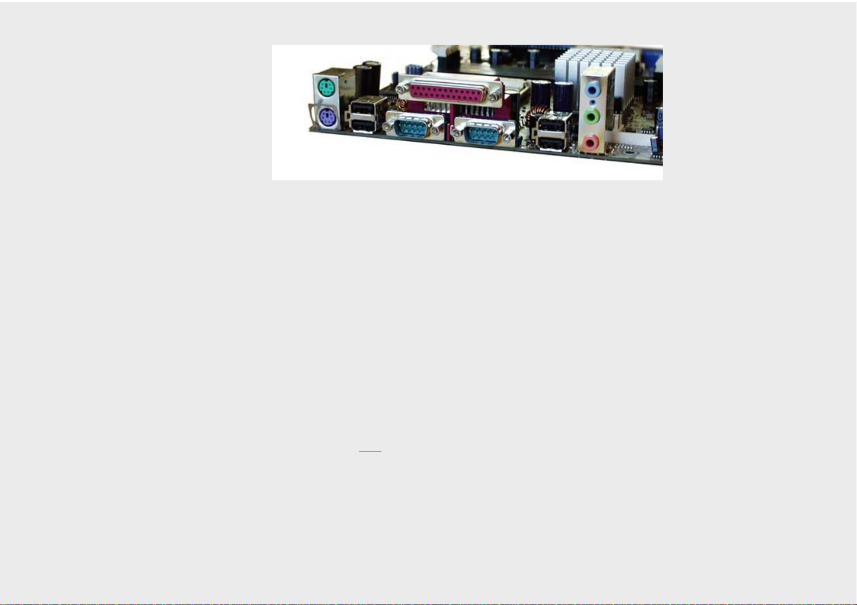
Heart of the new and improved VIA KT333A chipset is the KT333 NorthBridge (CD or higher reviwion)
On the other end of the seesaw, VIA Technologies have been spinning their own agenda, that is, shooting for being the number one
performance chipset supplier for the Socket A platform and they have done an extraordinarily good job. Granted that there are some
errata or insufficiencies in the IDE transfer as reported elsewhere but there are also some simple workarounds in the form of
increasing the PCI latency as long as the BIOS interface supports this option or else using the patch provided by George Breese to
change the PCI registers on the fly and accomplish the same net effect.
Still, the DRAM industry has been running off with performance of DDR ever since the introduction of the platform and why not use
the existing FSB scheme with a higher memory bus as done earlier with the Apollo and KX chipset series. In other words, there is a
new niche in the chipset market and there are new chipsets to fill it. The first revisions a.k.a. KT333 (chip markings lower than "CD")
were immediately replaced with the KT333A (chip markings CD and higher) and there are already a number of mainboards available
sporting the newest core logic revision.
We will have more on the different boards in the coming weeks, for now, we are going to start with the ASUS A7V333
next page: => At One Glance =>

LOSTCIRCUITS
SHORTCUTS:
Top Page
At One Glance
Features
Layout Ln-board
Peripherals
Jump, Jumper,
Jumperst
Dip Switch, Connectors
BIOS, Test
Configuration
SiSoft Sandra
Content Creation
WS2001, Expendable
Quake3 Arena, 3DMark
Overclocking,
Conclusion
Hot Offers for
the A7V333
ASUS A7V333
Hit me with the voltage regulators ..
(Review by MS, April 24, 2002)
At One Glance

ASUS A7V333
VIA KT333 (KT333-VT8233), 5 PCI, Promise RAID 0,1, CMedia 6 channel sound, Onboard Firewire
CPU interface
●Socket 462 for AMD Athlon (Thunderbird / Palomino / Duron) processors
Chipset

●VIA KT333 DDR chipset
●VIA KT333 (CE) North Bridge
●VIA VT8233 South Bridge
●VLink 266 MB/sec high speed interconnect
FSB, Multiplier and Voltage Settings
●1 MHz micro stepping in BIOS 100-230 MHz with automatic PCI divider adjustments from 1/3 to 1/5 as a function of FSB
frequency
●Multiplier settings in BIOS (6-14 x)
●Vre: 1.675- 2.3V via jumpers, Default, +0.025 +0.05 in BIOS
●V DDR 2.6V - 3.06V via jumpers
System Memory
●3 184 pin DIMM slots supporting 64MB to 1GB DDR DIMMs for maximum 3GB system memory
●DRAM operating mode: By SPD, manual
Memory Adjustment Settings
●CPU: DRAM ratio (1:1, 4:5)
●CAS latency: 2, 2.5
●tRCD: 2, 3
●tRP: 2, 3
●tRAS: 5T, 6T
●Bank Interleave: disabled, 2 bank 4 bank
●DRAM Command Rate: 2T, 1T
●Burst Length: 4 QW (quad words, 1 QW= 4 bytes = 32 bits), auto
●DQS I/O delay (in [Hex] values)
●Drive Strength (in [Hex] values)
Expansion Slots
●1 AGP (4x) slot
●5 32 bit PCI slots (manual assignment of IRQ Int 1-4)
Sound
●CMedia CM8738 6-channel audio onboard

BIOS
●Award Medallion BIOS
●PC-99, PnP, ACPI, APM, DMI, Green support
I/O Interface
●2 x EIDE channels (up to four devices)
●PI/O mode 3,4,5, ATAPI, UDMA 33/66/100
●2 x IDE RAID 1,0 channels (up to four devices)
●1 x 3 mode floppy connnector
●2 x UART 16550 COM ports
●1 x SPP, EPP, ECP LPT port
●1 x PS/2 mouse, ATX keyboard port
●6 x USB ports (2 back panel, 4 front panel USB headers)
●1 x IrDA
●1 x Line-out, Line-in, Mic-in,
●1 x Game MIDI port on separate back panel bracket
●1 x SPDIF connector
●1 x Line I/O header
●1 x AFPANEL (iPanel)
●1 x AAPANEL (iPanel sound)
●1 x SMBus
●1 x Secure Digital memory interface
●1 x memory Stick
●1 x Smart Card Reader
●1 x IEEE 1394 Firewire connector
Hardware Monitoring and Power Saving
●V core, V I/O, board voltage Fan rpm, CPU and system temp
●Power Saving LED
Form Factor and Dimensions
●ATX
●304 x 245 mm
next page: => What You Get =>

LOSTCIRCUITS
SHORTCUTS:
Top Page
At One Glance
Features
Layout Ln-board
Peripherals
Jump, Jumper,
Jumperst
Dip Switch, Connectors
BIOS, Test
Configuration
SiSoft Sandra
Content Creation
WS2001, Expendable
Quake3 Arena, 3DMark
Overclocking,
Conclusion
Hot Offers for
the A7V333
ASUS A7V333
Hit me with the voltage regulators ..
(Review by MS, April 24, 2002)
What you get
ASUS has never been stingy about the bundle shipped with their mainboards and even though some of the stuff included was not as
fancy as what some competitors offered, the included documentation, hardware and driver support was never anything short of
exemplary. Along this tradition are the features of the A7V333, there are some old acquaintances as the custom tailored I/O shield
which is needed since the ATX I/O connector block is non-standard. Standard features also include the manual and install CD along
with the little bag with extra jumpers and two 80 ribbon UATA cables and the mandatory floppy cable. Here it is, though where the
standard features end. In terms of documentation, ASUS has added a Quick Reference Card that, at one glance, shows the A7V333
by numbers. Unfortunately, though, there is no legend to explain the numbers, a small but potentially painful and at least puzzling
omission. Another quick setup guide in a gazillion of languages makes sure that worldwide distribution of the board is not hindered by
language barriers.
The lack of the explanatory collateral for the Quick Reference Card is more than made up for by the included sticker with all
mainboard settings and jumpers, that is, as long as they are documented at all. The sticker further contains the settings for the 6 x
dip switch that can be used to manually select the external CPU frequency (a better description than Front Side Bus which is a
Pentium2 legacy) from 100 MHz all the way up to 230 MHz. The sticker also features descriptions of all jumpers except for JP1 and
JP2, we will have more on those later.

The ATX I/O connector block is non-standard and leaves out the Game Port in favor of an additional USB 2.0 dual port which is
certainly more useful than the legacy interface.
In terms of additional hardware, the A7V333 ships with an extra dual port USB 2.0 bracket, which further sports the game port
missing in the I/O panel. Moreover, ASUS includes an IEEE 1394 connector bracket, certainly a much appreciated novelty in the
mainboard world.
The manual is typical ASUS quality, well organized and to the point, even though the checklist did not (for the first time with ASUS)
match the shipping contents in that the firewire module is not listed at all and the second 80 wire ribbon cable was listed as 40 ribbon
cable. Interestingly, the IEEE 1394 module is not mentioned with a single word in the manual at all. One sheet (2 pages) with last
minute additions / errata addresses the lack of STR support in Jumper Enable mode and a few other small errors.
We still found some interesting statements in the manual as for example: Overclocking the processor is not recommended. It may
result in a slower speed.
In the BIOS section, the manual falls short with some of the new settings for DDR control which are all thrown into the same pot
labeled Useful Test Parameters and show the options in Hex code values from 0 to F. We won't hold this against ASUS, though, for
the user it is best to leave those settings at Auto.
Quality
We have said it before and we can only repeat it here again, so far, we have yet to find an issue with quality on any ASUS board that
has gone through here. One of our criteria has always been the on-board power circuitry and the rule of thumb is that the more
phases we have, the cleaner is the power and the faster the switching as we documented in numerous earlier reviews. However,
there are also design differences that come into play, in that most standard power regulation circuits are organized into three
separate levels, that is, the main controller signaling to the driver chips which, in turn, drive the switch voltage regulators or
MOSFETs. So much for the standard layout used by Intersil and SemTech. With three phases, this is a great concept and suffices for
most CPUs. However, the intrinsic limitations of the design is the above described separation into three operational and physical

levels. The connectivity between the individual levels has to abide by the laws of electronics, meaning that operating frequency and
trace resistance result in rather high impedances which are putting a ceiling on the real world switching capabilities even if all
components used are capable of running much faster.
A possible workaround is to integrate the control circuitry and the driver chips into the same IC, a design recently pioneered by
OnSemiconductors. The lack of traces allows much faster regulation by means of mechanisms like early cycle termination so that
effectively, the integrated 2 phase design is functionally roughly equivalent to a standard four-phase design. It certainly speaks for
ASUS to see the OnSemi NCP5322A controller chip as the heart of the A7V333, providing a state of the art solution for fast and
smooth power regulation.
next page: => Overall Layout, Integrated Peripherals =>
General disclaimer: This page only reflects the author's personal opinion and assumes no responsibility whatsoever
regarding any of the contents or any damages that may occur explicitly or implicitly from reading the contents of this site. All names
and trademarks mentioned in this review are the exclusive property of the respective parent companies.
All contents of this site are protected by international copyright laws. Reproduction of the contents even in parts is not allowed
except after written permission by the author and referral to this site.
Copyright 2002 LostCircuits

LOSTCIRCUITS
SHORTCUTS:
Top Page
At One Glance
Features
Layout Ln-board
Peripherals
Jump, Jumper,
Jumperst
Dip Switch, Connectors
BIOS, Test
Configuration
SiSoft Sandra
Content Creation
WS2001, Expendable
Quake3 Arena, 3DMark
Overclocking,
Conclusion
Hot Offers for
the A7V333
ASUS A7V333
Hit me with the voltage regulators ..
(Review by MS, April 24, 2002)
Overall Layout
A direct comparison between the A7V333 and its predecessor A7V266-E shows a few similarities but also quite a few deviations of
the new board from the older one. The most prominent change is the obliteration of active cooling of the North Bridge in favor of the
same bulky passive heatsink that also decorates the A7M266D. What has not changed is the general arrangement of components
and standard connectors. In short, we still find the CPU socket in N-W orientation and extremely close to the three DIMM slots. We
still see the two standard IDE ports below the two RAID channels enabled by a Promise controller and the floppy drive connector
horizontally oriented at the bottom of the PCB. Also, we still have five PCI and one AGP Pro slot. Unchanged are the position of the
ATX power connector and the standby power LED as well.
That is pretty much where the similarities end, though. The promise PDC 20256 controller has been replaced by the PDC 20276 chip
with extended UATA/133 capabilities, the ACR seen on the A7V266-E has disappeared completely and instead we have a whole
variety of new interfaces. Bottom line is that we are looking at an entirely new PCB which has carried over a few of the design rules
of the earlier version but shows otherwise a completely new face, especially in the lower half.

VIA USB 2.0 Controller
Thus far, USB 2.0 has been the domain of NEC with their different variations of USB2.0 controller chips in QFP or BGA format. This
will certainly change in the near future since VIA's own USB controller chip (VT6202) has rolled out a few weeks ago and will, by
sheer convenience, replace the NEC IC on VIA chipset-based mainboards. The A7V333 is the first board where we see this
particular on-board USB 2.0 interface but it'll move into the mainboard field very fast.
CMedia Onboard Sound
The 6-channel CMI8378 chip has almost become a commodity with high-end mainboards and the only serious competition is the on-
board Sound-Blaster as seen on some GigaByte boards. The sound quality is more than acceptable and makes any additional sound
card rather superfluous which is just another reason for the above-mentioned lack of the ACR slot, there is simply no need for
another, software-based audio interface.
The included backpanel bracket features two IEEE 1394 Firewire ports. The wide connector on the cable plugs into the mainboard
IEEE 1394 connector.
IEEE 1394 OnBoard Firewire
A novel integrated peripheral is the on-board IEEE 1394a Firewire using the TexasInstruments TSB43AB21 chip. This IEEE 1394a
integrated link controller and physical layer (PHY) device features an integrated 400-megabit per second (Mbps) 1-port compatible
with version 1.1 of the Open Host Control Interface (OHCI) specification. Intelligent integrated power management and a 1.8-V core
operating voltage with universal PCI interfaces compatible with 3.3-V and 5-V PCI signaling environments make the TI controller the
probably most suitable IC for integrated Firewire. Keep in mind that this particular chip only features a single port. This also means
that one needs to make a decision which of the two interfaces offered on the bracket will be used since the cable can only be
connected to one of the two interfaces at the time.

LOSTCIRCUITS
SHORTCUTS:
Top Page
At One Glance
Features
Layout Ln-board
Peripherals
Jump, Jumper,
Jumperst
Dip Switch, Connectors
BIOS, Test
Configuration
SiSoft Sandra
Content Creation
WS2001, Expendable
Quake3 Arena, 3DMark
Overclocking,
Conclusion
Hot Offers for
the A7V333
ASUS A7V333
Hit me with the voltage regulators ..
(Review by MS, April 24, 2002)
Jumpers and Switches
In times where everybody follows the jumperless trend, it is a bit nostalgic to see a board featuring not one or two but a whole battery
of jumpers. Suffice it to say that under many conditions, jumpers and switches are much preferable over any software (including
BIOS)- based solution. The minor inconvenience caused by a one time enabling disabling of certain integrated peripherals is no
comparison to the nuisance of a PnP OS constantly searching for additional hardware that was disabled in the BIOS but still spooks
around in the background. In other words, the true art is to find a compromise between features that make sense to support in
SoftBIOS mode and those that are better off by the unambiguous ways of hard setting.
Jump, Jumper, Jumperest
Despite the fact that the A7V333, once it is up and running can be operated in jumper-free mode, the board features a gazillion of
jumpers meant to enable / disable RAID, on-board sound, IEEE 1394 Firewire, USB and Keyboard Power-Up, the Secure Digital and
Memory Stick media interfaces and the infamous POST Reporter which comments on the different boot processes (the last thing I

personally would need but then, some like it). All in all, ASUS deserves a high commendation for this solution since it is independent
of the BIOS revision and plain and simply cleaner than any soft solution. Needless to say that these jumpers don't really need any
further description, the same holds for the audio bass center setting.
A small "Hors d'Oeuvre" of the jumper menu awaiting the un-expecting user of the A7V333: on the left are JP1 and JP2 to set the
DDR voltages. "1" enables Power-On by USB 1 and 2, "2" and "3" are the line audio header jumpered to reroute the signals to the
back panel jacks and the bass center setting, respectively. "4" and "5" are audio and Firewire enable. The Firewire connector is
partially visible next to the VDDR jumpers. Also in the picture are the dip switch to manually set FSB frequency, the USB 2.0 header
enabled by the VIA VT6202 controller chip. On the left of the USB chip is the TI IEEE 1394 controller, on the right is the CMedia
CMI8738 6-channel sound.
There are a few other jumpers on board that deserve more attention. First, there is the known JEN jumper to enable / disable jumper-
free mode. By default, jumper-free is enabled, however, in order to e.g. access the dip switch, the jumper needs to be moved.
The VID1-4 header allows hard setting of the CPU core voltage from 1.675 to 1.85V with two voltage outputs, depending on which
CPU type is used. In order to really burn up the CPU, though, it is necessary to move the Voltage Regulator Output Limit jumper to
the Unlimited position. In addition, the A7V333 features an undocumented Overvoltage jumper. The same jumper on the P4B266
opens up additional Vre settings in the soft BIOS, in the A7V333, moving the Overvoltage jumper simply increases the Vre by 0.3V,
that is, if the Voltage Regulator Output Limit is set to "unlimited". Consequently, if the Vre is set to 1.75, the real Vre as shown by the
Hardware Monitor is 2.05V. Better be careful with this one.

It gets more confusing with the ROMSIP jumper. The manual states: This jumper selects the source for data to set functional
parameters fir the CPU. The default setting [1-2], enables present ROM data access from the chip. Resetting the jumper to [2-3]
enables the use of BIOS to set CPU parameters. Phil Marlowe once said to me: Dead men don't wear plaid. That was 20 years ago
and I still have no clue what it means. We may have some more info on this matter shortly, so stay tuned.
DDR Voltages
When it comes to running voltages out of spec, hardly any manufacturer has the kind of track record as ASUS. From the P5A to the
A7M266, the road has literally been paved with burned DIMMs and the A7V333 threatens to continue this tradition.
The layout of the VDDR jumpers has been carried over from the A7V266-E, that is jumpers JP1 and JP2, only the values have
changed. By default, the A7V333 supplies a whopping 2.78-2.85 VDD and VDDQ (DDR core and I/O voltage). The variation
accounts for the differences in measurement on several boards. Changing the jumper configuration allows settings between 2.59 and
3.06V. The detailed settings are:
ii 2.59 - 2.63V (same with one or both jumpers removed completely)
i! 2.78 - 2.85V (default setting, out of spec according to JEDEC guidelines)
!i 2.88 - 2.96V
!! 2.95 - 3.06V
The latter two settings are almost guaranteed to destroy the memory modules, maybe not today but after a few weeks. It is not clear
what the purpose of the high voltage settings is, however, it is only a matter of time until this will become a liability issue for ASUS,
one way or another. Keep in mind that the settings are not documented and the high settings are not meant for "public consumption"
by ASUS either.
The interesting thing about these settings is that all current high-end DDR chips are using internal voltage regulators to reduce the
core voltage to 1.8V which is necessary to run at high frequency. The only parts of the chips that actually see the increased voltage
are input/ output buffers and, granted that those will wiggle a bit faster at higher voltages, the net effect is counteracted by the fact
that the internal voltage regulators produce a lot of heat that will overall slow down the chips. In other words, a sensitive approach
would be to leave VDD alone but increase VDDQ. Admittlely, there are some older DIMMs that will run at 2.5V internally but those
will hardly be used in PC2700 mode of operation which is the only scenario where the massive overvoltage would be of benefit.
The recommendation in this case is, similar as what we suggested for the A7M266: simply take off both JP1 and JP2 to bring the
voltages back to where they belong. Side effects are that the failure rate, that is, stuck bits and system crashes in memory-intensive
applications go down quite dramatically. In addition, we saw up to 3 % system performance increase in Expendable at the lower
voltage. It is not completely clear what causes this performance increase but any electronics will run faster and cleaner when they
run cooler.
next page: => Dip Switch, Connectors =>

LOSTCIRCUITS
SHORTCUTS:
Top Page
At One Glance
Features
Layout Ln-board
Peripherals
Jump, Jumper,
Jumperst
Dip Switch, Connectors
BIOS, Test
Configuration
SiSoft Sandra
Content Creation
WS2001, Expendable
Quake3 Arena, 3DMark
Overclocking,
Conclusion
Hot Offers for
the A7V333
ASUS A7V333
Hit me with the voltage regulators ..
(Review by MS, April 24, 2002)
Dip Switch
Above, we already mentioned the JEN jumper and its function to enable/ disable jumperless mode. One of the gizmos depending on
the JEN-jumper is the dip switch that can be used to manually assign the following frequencies to the external CPU bus [in MHz]:
●100
●133
●140
●150
●166
●170
●180
●190
●200
●220
●230
Unfortunately, there is no documentation about what happens to the PCI bus at the higher frequency settings, however, the soft
BIOS shows switching from the 1/3 to the ¼ divider at 120 MHz and further to the 1/5 divider at 160 MHz.

Connectors
The number of jumpers on the A7V333 is only exceeded by the number of on-board connectors. We have the standard audio I/O
connectors backed by two line-out / line-in headers, both jumpered by default to route the audio signals to the I/O backpanel. A
Digital audio interface is provided in form of the SPDIF header
A back panel bracket featuring the gameport and two USB 2.0 / 1.1 ports acts as substitute for the missing gameport in the ATX I/O
panel.
Other connectors include infrared (SIR + CIR), SMBus, chassis intrusion and thermal sensor. The missing game port can be installed
via the game port connector at the bottom of the PCB, next to the Smart Card Reader header. For those who still need additional
USB ports, the A7V333 features an extra USB1.1 header which is pin-compatible with the USB 2.0 standard so that the bracket
included with the shipping content can be hooked up to either header.
Specialty connectors are the interface for the IEEE 1394a Firewire port and the SD / MS (secure digital and memory stick) smart
media headers that can connect to the appropriate reader. Somewhat surprising is that only 3 fan connectors are found on the board.
In addition, the A7V333 features the proprietary ASUS iPanel Interface as well as the AFPanel (Audio Front Panel)

LOSTCIRCUITS
SHORTCUTS:
Top Page
At One Glance
Features
Layout Ln-board
Peripherals
Jump, Jumper,
Jumperst
Dip Switch, Connectors
BIOS, Test
Configuration
SiSoft Sandra
Content Creation
WS2001, Expendable
Quake3 Arena, 3DMark
Overclocking,
Conclusion
Hot Offers for
the A7V333
ASUS A7V333
Hit me with the voltage regulators ..
(Review by MS, April 24, 2002)
BIOS
As in all current ASUS mainboards, the A7V333 features the Award Medallion BIOS interface. For most parts, the BIOS is rather
standard, multiplier settings are offered up to 14x which, of course, will only work with an unlocked CPU. What we found with the
XP2100+, though was that selection of lower multiplier values was simply ignored whereas setting of 13.5 and 14x would result in
POST failure.
With the original 1005 BIOS, we experienced all sorts of stability problems, however, the latest (1006) BIOS solved all those
problems. One new setting in the Advanced menu is the System Performance that can be set to Optimal and Turbo, with Turbo being
somewhat faster but also less stable.
The main difference to any of the previous ASUS BIOS versions is the fact that something, somewhere must have gotten a bit out of
hand. What I am referring to is the fact that the BIOS offers a ton of different settings to adjust the Input and output strobe delay
(DQS) and similar parameters as S2K and DQS driving strength. To make a long story short, the values are given in [Hex] format and
personally, I would not recommend messing around with them since there is no telling what changing the settings will really do to the
system. Quite honestly, there is also no reason at all to make these settings user-accessible unless one is fishing for eye candy.

to "disabled".
All other settings are standard, the BIOS offers soft setting of Vre (in four increments of 0.025 each over the default value), External
CPU speed adjustments from 100 to 230 MHz in 1 MHz steps (PCI divider switching at 120 and 160 MHz to ¼ and 1/5, respectively)
and the usual memory timing adjustments as there are CAS latency, RAS-to-CAS Delay, Precharge and RAS Active Time. More
settings comprise the chip select command rate disguised here as 1T CMD Rate with the options of enabled / disabled.
Compared to the original KT266 (A) chipset, the new addition is the option of running the memory in asynchronous mode, that is
maintaining a 133 MHz FSB while the memory bus is running at 166 MHz. Needless to say that in most cases, this will require higher
latencies and, on a hardware level, the involvement of fifos (first-in-first-out) pipelines and synchronizers that will take their toll on the
overall performance. The respective setting in the BIOS is the CPU/Memory frequency ratio that can be set to either 1:1 or 4:5.
The Hardware Monitor shows CPU and Mainboard temperatures as well as fan rotational speeds and Vre, 12V, 5V and 3.3V.
Test Configuration
Hardware
●ASUS A7V333
●AMD Athlon XP2100+
●1 x 512 MB Mushkin PC2100 Level 2 DDR
●ATi Radeon 8500
●IBM 60GXP (20.5GB)
●ASUS 40x CDROM
●Intel 10-100T Fast Ethernet adapter
●Alps Electric Floppy Drive
Software
●Windows2000 Professional
●W2K Service Pack2
●ATi W2K 6058 drivers (beta)
Installation and Setup
Physical setup is no problem at all, courtesy of the excellent Driver CD. As touched upon briefly already, the original 1005 BIOS had
caused some stability issues that were completely resolved with flashing to the 1006 version. The only issue that popped up in this
case was an error message at the end of the POST stating:
Error: Can't write ESCD
This issue was resolved by enabling "Reset Configuration Data" in the BIOS once, after which the value defaulted back automatically
to "disabled".

conditions that are limited mostly by the page size and Page Hit limitations (if those are imposed by the controller). With an optimized
path, current high-end systems are capable of achieving up to roughly 95% bus utilization. That is, with a PC2100 interface,
bandwidth rates of 2050 are not uncommon. The big question is, how the asynchronous memory bus behaves under these
conditions, especially since, as mentioned above, the CPU bus cannot handle more than 2100 MB/sec in the first place.
LOSTCIRCUITS
SHORTCUTS:
Top Page
At One Glance
Features
Layout Ln-board
Peripherals
Jump, Jumper,
Jumperst
Dip Switch, Connectors
BIOS, Test
Configuration
SiSoft Sandra
Content Creation
WS2001, Expendable
Quake3 Arena, 3DMark
Overclocking,
Conclusion
Hot Offers for
the A7V333
ASUS A7V333
Hit me with the voltage regulators ..
(Review by MS, April 24, 2002)
Performance
Memory Subsystem / SiSoft Sandra 2002
As already mentioned, running the memory bus at 166MHz or at 5:4 harmonics of the external CPU bus requires some mechanisms
to translate the higher memory speed to the same data rate at which the EV6 bus is running. These mechanisms include serially
connected buffers that accept the data on one end and spit them out at the other side. Suffice it to say that each buffer stage requires
an extra clock cycle until the data are forwarded, in other words, the extra latencies eat up a substantial amount of bandwidth.
Exacerbating is that, since the CPU bus runs at 266 Mbsp (Megabit/ sec and pin) and 64 bit width, there is an a priori limitation to
2100 MB/s between CPU and chipset that cannot be exceeded.
Buffering Enabled
Buffering Enabled essentially means that prefetching is allowed and the memory bus is operating under optimized, streaming

"Turbo" setting, increases the PC2100 performance beyond the highest scores we got out of PC2700 operation. Increasing the bus
frequency shows pretty much the same picture.
SiSoft Sandra Memory Benchmark results depending on BIOS settings and memory frequency. All results were obtained using the
"Optimized" setting unless indicated by "Turbo", all runs were done at 2:2:2, 1T CMD Rate and 6T tRAS except for those at 4:5 (CPU
: Memory Frequency) and SPD where the latencies were increased to 2.5:3:3, 1T CMD Rate and 6T tRAS. At the Optimal setting and
133 MHz memory bus, the bandwidth is slightly lower than at the 166 and SPD setting. Lowering the latencies at the 166 MHz setting
does not buy very much, consistent with the idea that the bottleneck is in the chipset rather than in the actual memory. Moving to the
Other manuals for A7V333
3
Table of contents
Other Asus Motherboard manuals

Asus
Asus CUR-DLSR User manual

Asus
Asus M4N68T LE V2 User manual

Asus
Asus PR-DLS User manual

Asus
Asus P4P800-VM User manual

Asus
Asus TUF GAMING B460-PLUS User manual

Asus
Asus P5-99B User manual

Asus
Asus GRYPHON ARMOR KIT User manual

Asus
Asus Pro H610M-CT D4 User manual

Asus
Asus 90MB0U00-M0EAY0 User manual

Asus
Asus P5N32-SLI SE DELUXE User manual

Asus
Asus ROG STRIX B360-F GAMING User manual

Asus
Asus A7VI-VM User manual

Asus
Asus Z170M-E D3 User manual

Asus
Asus EX-B760M-V5 D4 User manual

Asus
Asus M2N GREEN User manual

Asus
Asus KFN4-D16 1U User manual

Asus
Asus CUC2 User manual

Asus
Asus Rog Zenith II Extreme User manual

Asus
Asus B85M-F User manual

Asus
Asus ROG MAXIMUS XII EXTREME User manual