www.awinic.com 1 Copyright © 2022 SHANGHAI AWINIC TECHNOLOGY CO., LTD
Ultra-Low-EMI, RNS, Mono, Filter-Free,
Class-D Audio Amplifier
Features
EEE Function, Greatly reduces EMI over the
full bandwidth
Excellent Pop-Click Suppression
RNS (RF-TDD Noise Suppression)
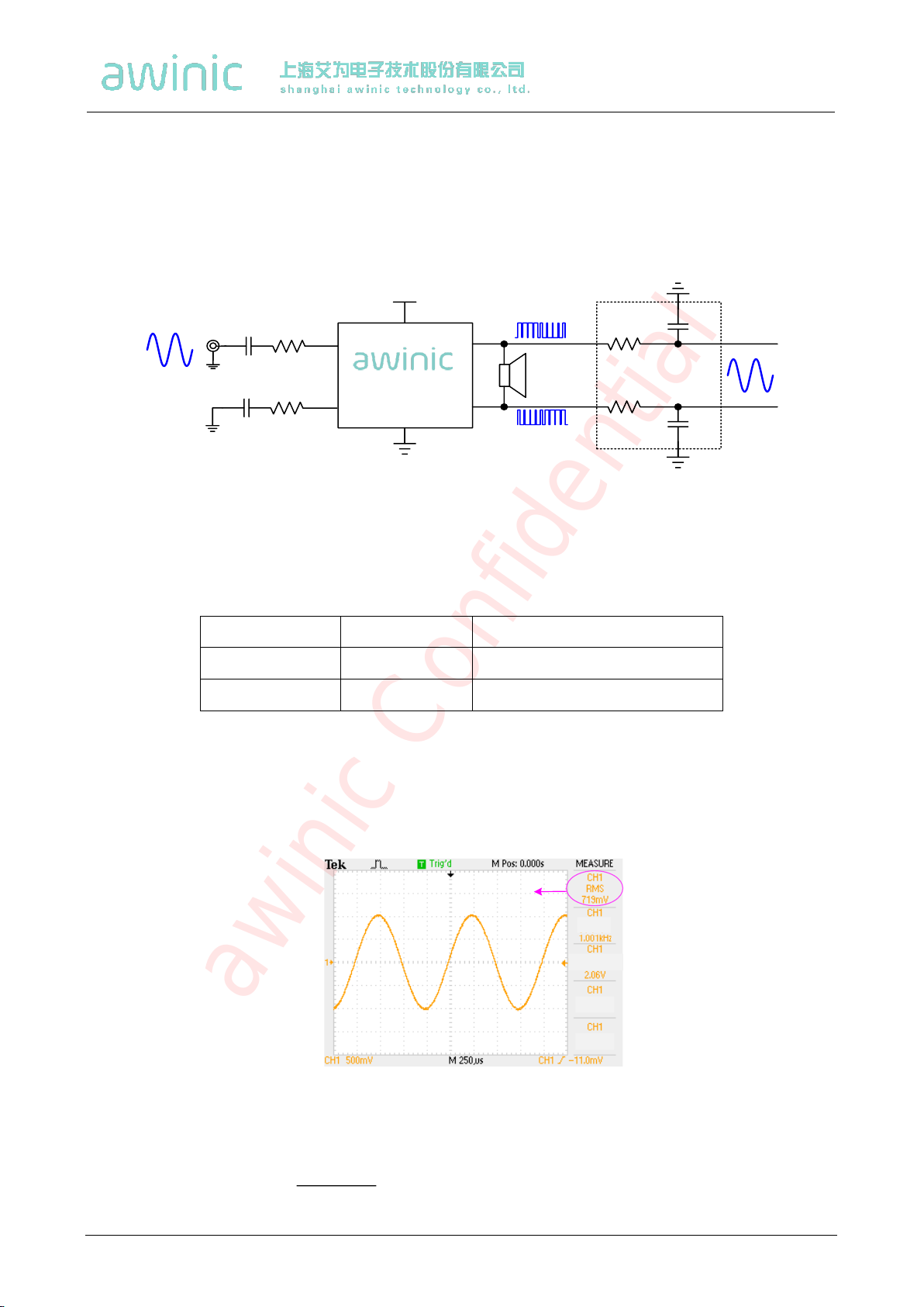
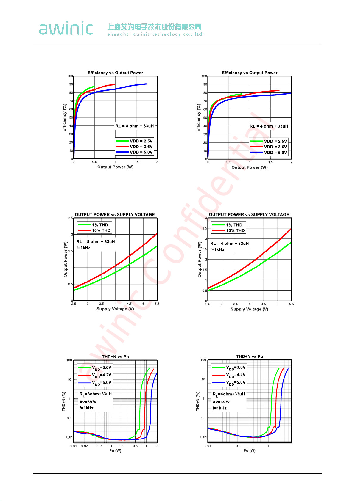
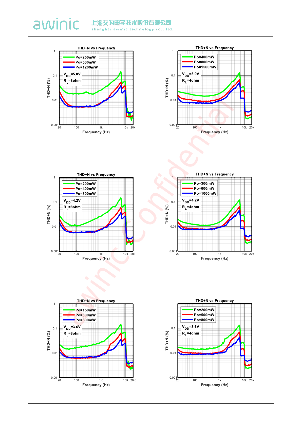
0.008%THD+N(Pout=0.4W,VDD=4.2V)
Filter-Free Class-D Architecture
Up to 90% Efficiency
High PSRR (75dB at 217Hz)
Low Quiescent Current (2.8mA)
Low Shutdown Current (<0.1A)
Power Supply Range: 2.5V~5.5V
Over-Current Protection
Over-Temperature Protection
Small FCQFN 1.5mmX1.5mm-9L Package
RoHS compliant, lead-free packages
Applications
Cellular Phones
MP3/PMP
GPS
Digital Photo Frame
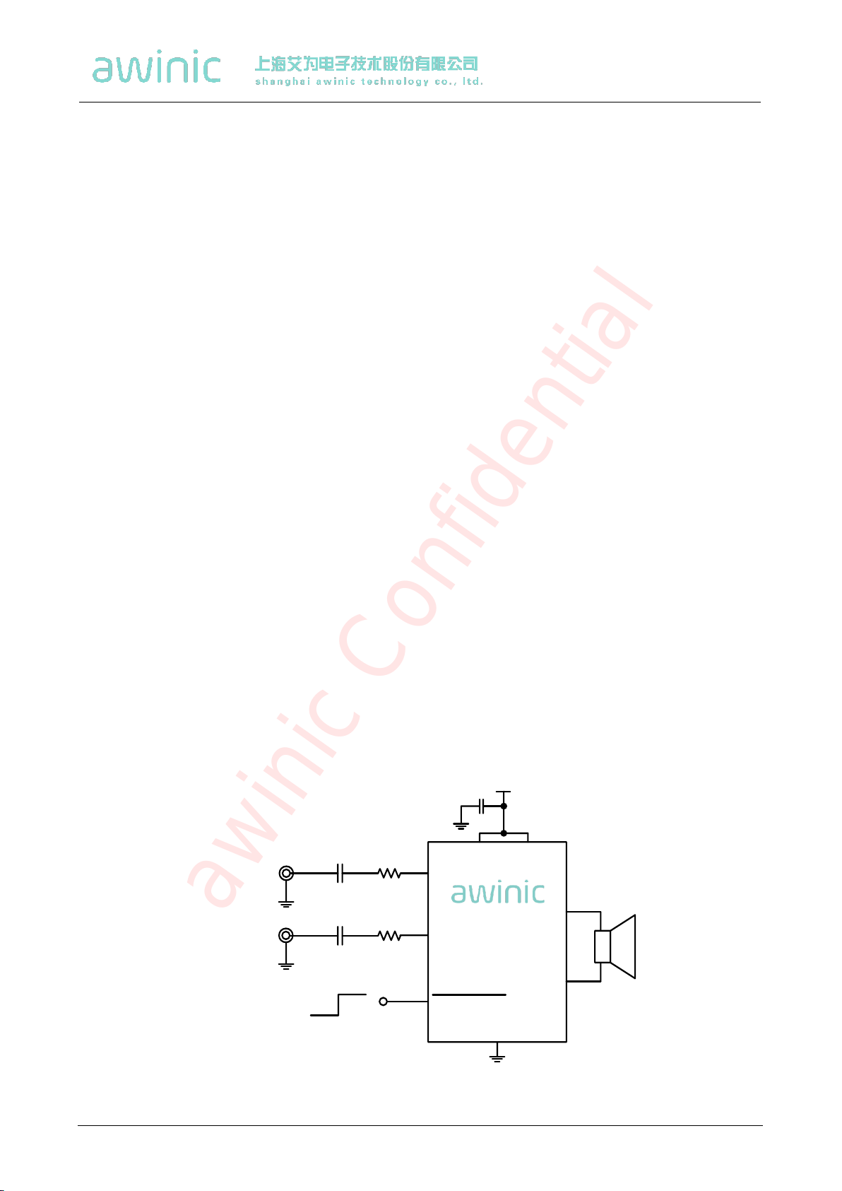
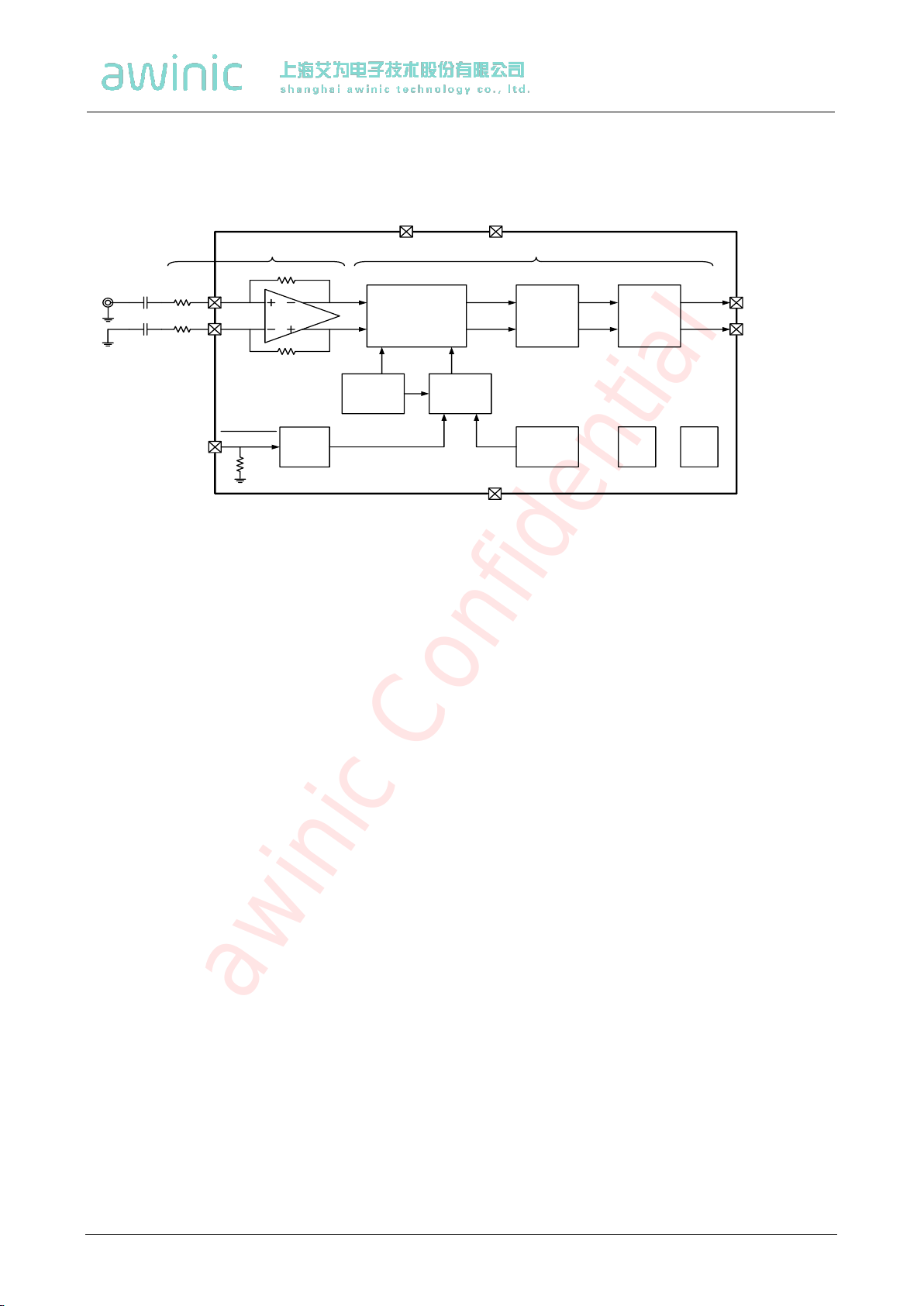
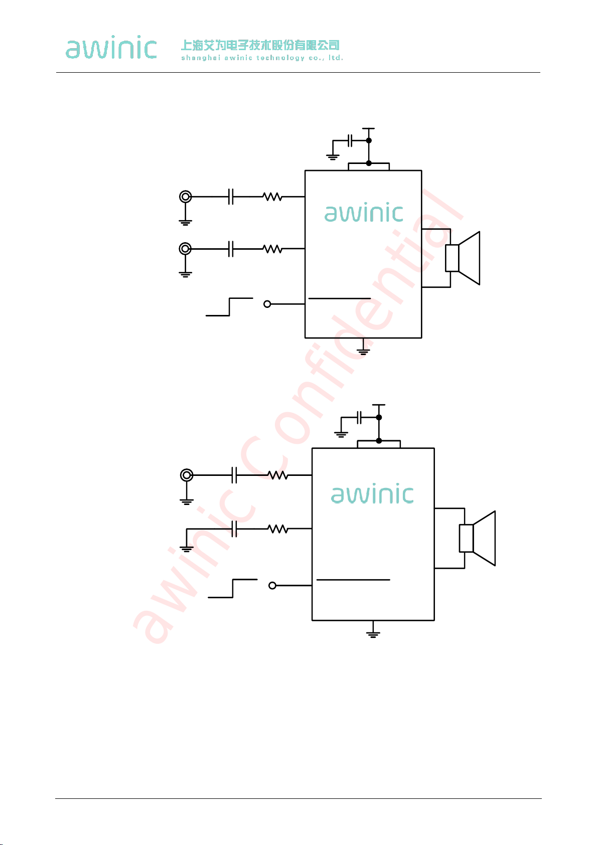
General Description
The AW8010B is a ultra-low-EMI,RNS, mono,
filter-free, Class-D audio amplifier. Unique RNS,
which effectively reduces RF energy, attenuate
the RF TDD-noise, an acceptable audible level to
the customer.
The AW8010B features the EEE (Enhanced
Emission Elimination) function which greatly
reduces EMI over the full bandwidth. The
AW8010B achieves better than 20dB margin
under FCC limits with 24 inch of cable.
The filter-free PWM architecture and internal
gain setting reduces external components count,
board area consumption, system cost and
simplifies the design. In addition, The AW8010B
offers efficiencies above 90%. The over-current
and over-temperature is prepared inside of the
device.
The AW8010B is available in an ultra small
FCQFN 1.5mmX1.5mmX0.55mm-9L package.
The AW8010B is specified over the industrial
temperature range of -40℃to +85℃.