AWINIC AW8155B User manual

AW8155B
Jul. 2022 V1.3
www.awinic.com 1 COPYRIGHT ©2022 SHANGHAI AWINIC TECHNOLOGY CO. LTD.
Non-Crack-Noise, Ultra-Low-THD+N, Ultra-Low-EMI,
Second Generation Class-D Audio Amplifier
Features
Ultra low THD+N:0.007%
AB/D operate mode
Two NCN level:0.65w and0.85w
Unique RNS
High SNR:95dB
EEE Function, Greatly reduces EMI over the
full bandwidth
Excellent Pop-Click Suppression
No VREF capacitor
Pin compatible with AW8155(A) AW8145
One-pulse control
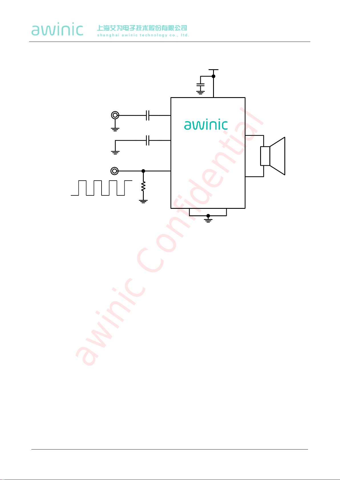
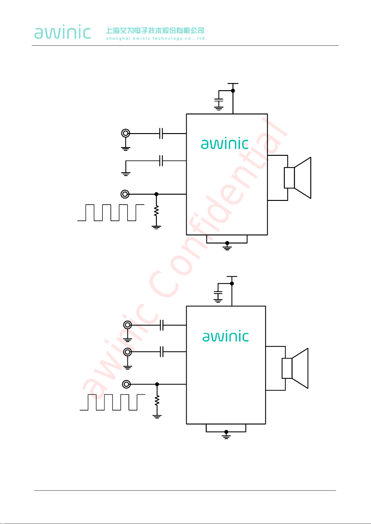
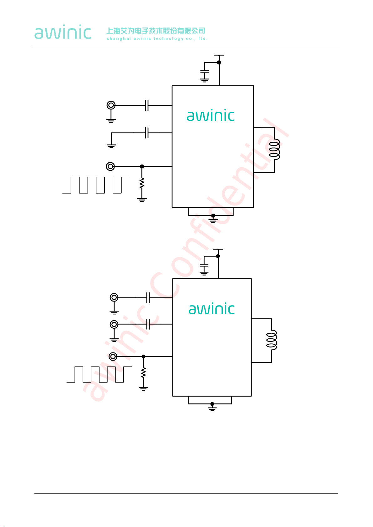
Filter-Free Class-D Architecture
High PSRR (75dB at 217Hz)
Low Shutdown Current (<0.1A)
Power Supply Range: 2.5V~5.5V
Over-Current Protection
Over-Temperature Protection
Small FCQFN 1.5mmX1.5mmX0.55mm-9L
Package
Applications
Cellular Phones
MP3/PMP
GPS
Digital Photo Frame
HAC ( Hearing Aid Compatibility )
General Description
The AW8155B is a non-crack-noise (NCN), ul-
tra-low-EMI, filter-free, AB/D output mode se-
lection, unique RNS technology, second gen-
eration Class-D audio amplifier. Ultra low
THD+N, Unique NCN function, which adjusts
the system gain automatically while detecting
the “Crack”distortion of output signal, protects
the speaker from damage at high power levels
and invites the user to bask in immense musical
enjoyment.
AW8155B NCN output power can be set to
0.65w or 0.85w for different speakers, this fea-
ture is embedded in order to protect speakers
from damage caused by an excessive sound
level.
The AW8155B features a unique RNS tech-
nology, which effectively reduces RF energy,
attenuate the RF TDD-noise, an acceptable
audible level to the customer.
The AW8155B features the EEE (Enhanced
Emission Elimination) function which greatly
reduces EMI over the full bandwidth. The
AW8155B achieves better than 20dB margin
under FCC limits with 24 inch of cable.
The filter-free PWM architecture and internal
gain setting reduces external components
count, board area consumption, system cost
and simplifies the design. The over-current,
over-temperature is prepared inside of the de-
vice.
The AW8155B is available in an ultra small
FCQFN 1.5mmX1.5mmX0.55mm-9L package.
The AW8155B is specified over the industrial
temperature range of -40℃to +85℃.
awinic Confidential

AW8155B
Jul. 2022 V1.3
www.awinic.com 2 COPYRIGHT ©2022 SHANGHAI AWINIC TECHNOLOGY CO. LTD.
Typical Application
VON
INP
AGND
VDD
VOP
INN
PGND
Cs
1μF
AW8155B
CTRL
Cin 33nF
Cin 33nF
GPIO
10k
Figure 1. AW8155B Application Schematic With Single-Ended Input
awinic Confidential

AW8155B
Jul. 2022 V1.3
www.awinic.com 3 COPYRIGHT ©2022 SHANGHAI AWINIC TECHNOLOGY CO. LTD.
Pin Configuration and Top Mark
INN CTRL
AGND AGND PGND
VOP
VDD
INP
123
A
B
CVON
1 2 3
A
B
C
A5A
XXX
A5A –AW8155BFCR
XXX - Production TracingCode
AW8155BFCR MARKINGAW8155BFCR TOP VIEW
Figure 2. Pin Configuration and Top Mark of AW8155B
Pin Definition
No.
Symbol
Description
A1
INP
Positive audio input
A2
VDD
Power Supply
A3
VOP
Positive audio output
B1
AGND
Analog ground
B2
AGND
Analog ground
B3
PGND
Power ground
C1
INN
Negative audio input
C2
CTRL
Shutdown and NCN control pin
C3
VON
Negative audio output
awinic Confidential

AW8155B
Jul. 2022 V1.3
www.awinic.com 4 COPYRIGHT ©2022 SHANGHAI AWINIC TECHNOLOGY CO. LTD.
Typical Application
VON
INP
AGND
VDD
VOP
INN
PGND
Cs
1μF
AW8155B
CTRL
Cin 33nF
Cin 33nF
GPIO
10k
Figure 3. AW8155B Application Schematic With Single-Ended Input
VON
INP
AGND
VDD
VOP
INN
PGND
Cs
1μF
AW8155B
CTRL
Cin 33nF
Cin 33nF
GPIO
10k
Figure 4. AW8155B Application Schematic With Differential Input
awinic Confidential

AW8155B
Jul. 2022 V1.3
www.awinic.com 5 COPYRIGHT ©2022 SHANGHAI AWINIC TECHNOLOGY CO. LTD.
VON
INP
AGND
VDD
VOP
INN
PGND
Cs
1μF
AW8155B
CTRL
Cin 33nF
Cin 33nF
GPIO
10k
HAC
Inductor
Figure 5. AW8155B HAC Application Schematic With Single-Ended Input
VON
INP
AGND
VDD
VOP
INN
PGND
Cs
1μF
AW8155B
CTRL
Cin 33nF
Cin 33nF
GPIO
10k
HAC
Inductor
Figure 6. AW8155B HAC Application Schematic With Differential Input
awinic Confidential

AW8155B
Jul. 2022 V1.3
www.awinic.com 6 COPYRIGHT ©2022 SHANGHAI AWINIC TECHNOLOGY CO. LTD.
Ordering Information
Part Number
Temperature
Package
Marking
Moisture Sensitivity
Level
Environmental
Information
Delivery Form
AW8155BFCR
-40℃~85℃
FCQFN
1.5mmX1.5mm
-9L
A5A
MSL3
RoHS+HF
3000
units/Tape and
Reel
Absolute Maximum Ratings(NOTE1)
PARAMETERS
RANGE
Supply voltage range VDD
-0.3V to 6V
Input voltage range
-0.3V to VDD+0.3V
Junction-to-ambient thermal resistance θJA
90℃/W
Operating free-air temperature range
-40℃to 85℃
Maximum operating junction temperature TJMAX
125℃
Storage temperature TSTG
-65℃to 150℃
Lead temperature (soldering 10 seconds)
260℃
ESD(Including CDM HBM MM)(NOTE 2)
HBM (human body model)
±2kV
CDM (charged-device model)
±1.5kV
Latch-Up
Test condition:
JESD78E
+IT:200mA
-IT:-200mA
NOTE1: Conditions out of those ranges listed in "absolute maximum ratings" may cause permanent damages to the de-
vice. In spite of the limits above, functional operation conditions of the device should within the ranges listed in "recom-
mended operating conditions". Exposure to absolute-maximum-rated conditions for prolonged periods may affect device
reliability.
NOTE2: The human body model is a 100pF capacitor discharged through a 1.5kΩ resistor into each pin. Test method:
ESDA/JEDEC JS-001-2017
Test method of the charged-device model: ESDA/JEDEC JS-002-2018
Operate mode description
(TA=25℃,VDD=4.2V,RL=8Ω+33uH)
mode
CTRL
operating
AV
(V/V)
NCN power
(W)
RNS
mode 1
Class_D
8
0.65
√
mode 2
Class_D
12
0.85
√
mode 3(Note)
Test
mode 4
Class_AB
12
/
Note: mode 3 is internal test mode
awinic Confidential

AW8155B
Jul. 2022 V1.3
www.awinic.com 7 COPYRIGHT ©2022 SHANGHAI AWINIC TECHNOLOGY CO. LTD.
Electrical Characteristics
Test Condition: VDD=3.6V ,TA=25℃, RL=8Ω+33uH,Cin=33nF,f=1kHz (Unless otherwise specified)
Parameter
Conditions
Min
Typ
Max
Units
VDD
Power supply voltage
2.5
5.5
V
VIH
CTRL high input voltage
1.3
VDD
V
VIL
CTRL low input voltage
0
0.35
V
VOS
Output offset voltage
Input AC grounded,VDD=2.5V to 5.5V
-30
0
30
mV
ISD
Shutdown current
VDD=3.6V,CTRL =0V
0.1
1
μA
fSW
Modulation Frequency
VDD=2.5V to 5.5V
600
800
1000
kHz
TSD
Thermal Protect level
160
℃
TSDR
Thermal Hysteresis
120
℃
TON
Start-up time
40
ms
Rini
Internal impedance
28.5
kΩ
PO
Output power
THD+N=10%,RL=4Ω+33uH,VDD=5V
2.66
W
THD+N=1%,RL=4Ω+33uH,VDD=5V
2.20
W
THD+N=10%,RL=8Ω+33uH,VDD=5V
1.60
W
THD+N=1%,RL=8Ω+33uH,VDD=5V
1.30
W
THD+N=10%,RL=4Ω+33uH,VDD=4.2V
1.94
W
THD+N=1%,RL=4Ω+33uH,VDD=4.2V
1.60
W
THD+N=10%,RL=8Ω+33uH,VDD=4.2V
1.13
W
THD+N=1%,RL=8Ω+33uH,VDD=4.2V
0.94
W
THD+N=10%,RL=4Ω+33uH,VDD=3.6V
1.40
W
THD+N=1%,RL=4Ω+33uH,VDD=3.6V
1.14
W
THD+N=10%,RL=8Ω+33uH,VDD=3.6V
0.84
W
THD+N=1%,RL=8Ω+33uH,VDD=3.6V
0.68
W
Mode 1
Iq
Quiescent current
VDD=3.6V,Input AC grounded, no load
3.0
mA
η
Efficiency
VDD=3.6V,Po=0.8W,RL=8Ω+33uH
91
%
Av
Voltage gain
7
8
9
V/V
PSRR
Power suppression ration
VDD=4.2V,Vp-p_sin=200mV
217Hz
75
dB
1kHz
72
dB
THD+N
Total harmonic distortion
plus noise
VDD=4.2V,Po=0.5W,RL=8Ω+33uH
0.007
%
VDD=3.6V,Po=0.25W,RL=8Ω+33uH
0.008
%
PONCN
NCN output power
f=1kHz,RL=8Ω+33uH,VDD=4.2V
0.65
W
TAT
Attack time(-11dB)
VDD=4.2V
45
ms
TRL
Release time(11dB)
VDD=4.2V
1
s
AMAX
Max attenuation
VDD=4.2V
-11
dB
Vn
Output noise
f=20Hz-20kHz,input AC grounded
53
uV
SNR
Signal-to-noise ratio
VDD = 5 V, PO = 1 W, RL = 8Ω+33uH
95
dB
awinic Confidential

AW8155B
Jul. 2022 V1.3
www.awinic.com 8 COPYRIGHT ©2022 SHANGHAI AWINIC TECHNOLOGY CO. LTD.
Parameter
Conditions
Min
Typ
Max
Units
Mode 2
Iq
Quiescent current
VDD=3.6V,Input AC grounded, no load
3.0
mA
η
Efficiency
VDD=3.6V,Po=0.8W,RL=8Ω+33uH
91
%
Av
Voltage gain
11
12
13
V/V
PSRR
Power suppression ration
VDD=4.2V,Vp-p_sin=200mV
217Hz
75
dB
1kHz
72
dB
THD+N
Total harmonic distortion
plus noise
VDD=4.2V,Po=0.5W,RL=8Ω+33uH
0.007
%
VDD=3.6V,Po=0.25W,RL=8Ω+33uH
0.009
%
PONCN
NCN output power
VDD=4.2V , RL=8Ω+33uH,f=1kHz
0.85
W
TAT
Attack time(-13.5dB)
VDD=4.2V
50
ms
TRL
Release time(13.5dB)
VDD=4.2V
1.2
s
AMAX
Max attenuation
VDD=4.2V
-13.5
dB
Vn
Output noise
f=20Hz-20kHz,input AC grounded
76
uV
SNR
Signal-to-noise ratio
VDD = 5 V, PO = 1 W, RL = 8Ω+33uH
93
dB
Mode 4
Iq
Quiescent current
VDD=3.6V,Input AC grounded, no load
3.5
mA
η
Efficiency
VDD=3.6V,Po=0.8W,RL=8Ω+33uH
78
%
Av
Voltage gain
11
12
13
V/V
PSRR
Power suppression ratio
VDD=4.2V,Vp-p_sin=200mV,
217Hz
70
dB
1kHz
68
dB
THD+N
Total harmonic distortion
plus noise
VDD=4.2V,Po=0.5W,RL=8Ω+33uH
0.2
%
VDD=3.6V,Po=0.25W,RL=8Ω+33uH
0.2
%
Vn
Output noise
f=20Hz-20kHz,input AC grounded
88
uV
SNR
Signal-to-noise ratio
VDD = 5 V, PO = 1 W, RL = 8 Ω+33uH
92
dB
one-wire pulse control
TH
CTRL high level hold time
VDD=2.5V to 5.5V
0.75
2
10
us
TL
CTRL low level hold time
VDD=2.5V to 5.5V
0.75
2
10
us
TLATCH
CTRL turn on delay time
VDD=2.5V to 5.5V
150
800
us
TOFF
CTRL turn off delay time
VDD=2.5V to 5.5V
150
800
us
awinic Confidential

AW8155B
Jul. 2022 V1.3
www.awinic.com 9 COPYRIGHT ©2022 SHANGHAI AWINIC TECHNOLOGY CO. LTD.
MEASUREMENT SETUP
AW8155B features switching digital output, as shown in Figure 7. Need to connect a low pass filter to
VOP/VON output respectively to filter out switch modulation frequency, then measure the differential output of
filter to obtain analog output signal.
VOP
VON
INP
INN
Rin
Cin
AW8155B
Rin
Cin 32kHz
Low-Pass Fliter
500Ω
500Ω
10nF
10nF
Figure 7. AW8155B test setup
Low pass filter uses resistance and capacitor values listed in Table 1.
Table 1 AW8155B recommended values for low pass filter
Rfilter
Cfilter
Low-pass cutoff frequency
500Ω
10nF
32kHz
1kΩ
4.7nF
34kHz
Output Power Calculation
According to the above test methods, the differential analog output signal is obtained at the output of the
low pass filter. The valid values Vo_rms of the differential signal as shown below:
Vo_rms
Frequency
Peak To Peak
NO Display
NO Display
Figure 8. Valid value of AW8155B output signal
The power calculation of Speaker is as follows:
2
L( _ )
P load impedance of the speaker
L
L
Vo rms R
R
=( : )
awinic Confidential

AW8155B
Jul. 2022 V1.3
www.awinic.com 10 COPYRIGHT ©2022 SHANGHAI AWINIC TECHNOLOGY CO. LTD.
Typical Operating Characteristic
awinic Confidential

AW8155B
Jul. 2022 V1.3
www.awinic.com 11 COPYRIGHT ©2022 SHANGHAI AWINIC TECHNOLOGY CO. LTD.
OUTPUT POWER vs VIN
OUTPUT POWER (W)
VIN ( Vp )
0.5
NCN
0.01
0.05
0.1
0.5
1
2
0.2 0.4 1 20.1
OUTPUT POWER vs VIN
OUTPUT POWER (W)
VIN ( Vp )
0.5
0.01
0.05
0.1
0.5
1
2
0.2 0.4 1 20.1
mode1
VDD=4.2V
f=1kHz
RL=8Ω+33μH
NCN
mode2
VDD=4.2V
f=1kHz
RL=8Ω+33μH
awinic Confidential

AW8155B
Jul. 2022 V1.3
www.awinic.com 12 COPYRIGHT ©2022 SHANGHAI AWINIC TECHNOLOGY CO. LTD.
NCN POWERvs SUPPLY VOLTAGE
Supply Voltage ( V )
NCN Output Power ( W )
0.00
0.10
0.20
0.30
0.40
0.50
0.60
0.70
0.80
0.90
1.00
3.4 3.6 3.8 4 4.2 4.4 4.6
RL=8Ω+33uH
f=1kHz
mode1
mode2
0.65w
0.85w
awinic Confidential

AW8155B
Jul. 2022 V1.3
www.awinic.com 13 COPYRIGHT ©2022 SHANGHAI AWINIC TECHNOLOGY CO. LTD.
Class_D start up time Class_D shutdown time
VOP & VON
10ms/div
CTRL
VOP & VON
50us/div
CTRL
VOP & VON
10ms/div
CTRL
VOP & VON
50us/div
CTRL
Class_AB start up time Class_AB shutdown time
Vin
VOP-VON
10ms/div
Vin
VOP-VON
200ms/div
NCN release timeNCN attack time
awinic Confidential

AW8155B
Jul. 2022 V1.3
www.awinic.com 14 COPYRIGHT ©2022 SHANGHAI AWINIC TECHNOLOGY CO. LTD.
Functional Block Diagram
AW8155B
PGND
INN
Input
Buffer
INP
Class-D
Modulator
EEE
Module
Output
Stage
CTRL NCN & System
Control
VDD
AGND
Oscillator OCP OTP
VOP
VON
Class-AB
RNS
Figure 9. Functional Block Diagram of AW8155B
awinic Confidential

AW8155B
Jul. 2022 V1.3
www.awinic.com 15 COPYRIGHT ©2022 SHANGHAI AWINIC TECHNOLOGY CO. LTD.
Operation
The AW8155B is a non-crack-noise (NCN), ultra-low-EMI, filter-free, AB/D output mode selection, sec-
ond generation Class-D audio amplifier. Ultra low THD+N, Unique NCN function, which adjusts the
system gain automatically while detecting the “Crack” distortion of output signal, protects the speaker
from damage at high power levels and brings the most comfortable listening experience to the custom-
ers.
AW8155B NCN output power can be set to 0.65W or 0.85W for different speaker, this feature is em-
bedded in order to protect speakers from damage caused by an excessive sound level.
The AW8155B features a unique RNS technology, which effectively reduces RF energy, attenuate the
RF TDD-noise, an acceptable audible level to the customer.
The AW8155B features the EEE (Enhanced Emission Elimination) function which greatly reduces EMI
over the full bandwidth. The AW8155B achieves better than 20dB margin under FCC limits with 24 inch
of cable.
The filter-free PWM architecture and internal gain setting reduces external components count, board
area consumption, system cost and simplifies the design. The over-current, over-temperature is pre-
pared inside of the device.
The AW8155B is available in an ultra small FCQFN 1.5mmX1.5mm-9L package. The AW8155B is
specified over the industrial temperature range of -40℃to +85℃.
One-wire pulse control
One wire pulse control technology only needs a single GPIO port to operate the chip, complete a variety of
functions, it is very popular in the area of the GPIO port shortage and portable systems.
When the control signal line is longer, because of the signal integrity or radio frequency interference problem,
it will produce the narrow glitch signal. Awinic one wire pulse control technology integrated the Deglitch circuit
in internal control pin, which can effectively eliminate the influence of the glitch signal, as shown in figure 10.
Deglitch
Glitch is eleminated
Control signal with glitch
CTRL
AW8155B
Figure 10. Awinic Deglitch function diagram
The traditional one wire pulse control technology still receives pulse signal from control port when chip is
startup, so when the master control chip (such as mobile phone BB) sends wrong pulse during normal oper-
ation, the system will enter into error states. AW8155B uses one wire pulse latch technology, after the master
control chip has sent pulses, the state will be latched, no longer receive the latter mis-sending pulse signals,
as shown in figure 11.
awinic Confidential

AW8155B
Jul. 2022 V1.3
www.awinic.com 16 COPYRIGHT ©2022 SHANGHAI AWINIC TECHNOLOGY CO. LTD.
STATE 4
TraditionalOne Wire
PulseControl
TLATCH
Shielding abnormal
pulsesignal
STATE 3
STATE 4 STATE 4
Anti-interference One
Wire PulseControl
Figure 11. Anti-interference One Wire Pulse Control Function Diagram
AW8155B select each mode by one-wire pulse control, as shown in figure 12. When CTRL pin pull high form
shutdown mode, there is one rising edge, AW8155B start to work and set Gain=18dB, NCN level=0.65W.
When high-low-high signal set to CTRL pin, there are two rising edges, AW8155B start to work and set
Gain=21.5dB, NCN level=0.85W. When there are three rising edges, internal test mode is enable. When there
are four rising edges, AW8155B start to work in Class AB mode, while gain is to be set 21.5dB.
As shown in figure 12, when CTRL pull down above 1ms, AW8155B will enter shutdown mode.
THTL
0.75us<TL,TH<10us
Mode 1
Mode 2
Mode 3
Mode 4
TOFF
Figure 12. One-Wire pulse control
When AW8155B work in different mode, PIN CTRL should be low above 1ms which make the AW8155B shut
down, Then series pulse make the AW8155B work in right mode.
MODE2 MODE4
1ms
CTRL
Figure 13. One-wire pulse mode switch
RNS (RF TDD Noise Suppression)
TDD Noise Causes
GSM cell phones use TDMA (Time Division Multiple Access) slot sharing technology. The time is divided into
periodic frames in TDMA, and each frame is subdivided into a plurality of time slots. In order to transmit sig-
awinic Confidential

AW8155B
Jul. 2022 V1.3
www.awinic.com 17 COPYRIGHT ©2022 SHANGHAI AWINIC TECHNOLOGY CO. LTD.
nals to the base station, the signals sent from the base stations to the plurality of mobile terminals are ar-
ranged in a predetermined time slot in the transmission. In this case, each TDMA frame contains 8 time slots,
the entire frame is about 4.615ms long, and each slot time is 0.577ms.
With GSM handset, the RF power amplifier will transmit once every 4.615ms (217Hz), and the signal will
produce intermittent Burst current and strong electromagnetic radiation. Intermittent Burst current will form a
power fluctuation of 217 Hz; High frequency (900MHz and 1800MHz) RF signals form a 217Hz RF envelope
signal. 217Hz power fluctuations will be conducted through the conduction to the audio signal path, 217Hz RF
envelope signal will be coupled through the radiation into the audio signal path, if the protection is not good, it
will produce an audible TDD Noise, which includes the 217Hz noise And a harmonic noise signal of 217 Hz.
VBAT
Voltage
RF
Signal
4.615ms
Figure 14. Schematic Diagram of Power Supply Voltage and RF Signal during GSM RF Operation
RNS fully inhibit the conduction and radiation interference by the AWINIC unique circuit architecture. Effec-
tively improve the ability to suppress TDD Noise.
Conduction noise suppression
When the RF power amplifier is operating, it will draw the current from the battery by 217Hz frequency, Power
supply will be introduced to 217Hz power ripple since the battery has a certain internal resistance, it will be
coupled to the speaker through the audio power amplifier. The ability to suppress power fluctuations depends
on the PSRR of the audio power amplifier.
ac
ac
vdd
PSRR 20log( )
vout
=
Due to the input and output of the fully differential amplifier is perfectly symmetrical, theoretically, the effect of
the power supply fluctuation on the two outputs is exactly the same, and the differential output is completely
unaffected by the power supply fluctuation. In practice, due to process bias and other factors, the amplifier will
have a certain mismatch, PSRR is generally better than 60dB, it shows the output relative to the power fluc-
tuations can be reduced by 1000 times, such as 500mVp power fluctuations, the differential output of 0.5 mV,
which basically can meet the application requirements.
But in practical applications, the power amplifier may encounter conduction of TDD Noise problem even if its
PSRR is 60dB or 80dB, why is this? Because we also need to consider the impact of peripheral power mis-
matches of audio power amplifiers
awinic Confidential

AW8155B
Jul. 2022 V1.3
www.awinic.com 18 COPYRIGHT ©2022 SHANGHAI AWINIC TECHNOLOGY CO. LTD.
For conventional audio power amplifiers, when the input resistor Rin and the input capacitor Cin mismatch,
will greatly affect the audio power amplifier PSRR indicators, in the case of 24dB gain, PSRR will be weak-
ened to 46dB or so if the input resistance and Capacitor with 1% mismatch. PSRR will be weakened to 28dB
or so if the input resistance and input capacitance mismatch with 10% mismatch, when the power fluctuations,
it is easy to produce audible TDD Noise.
In order to enhance the audio power amplifier PSRR in the input resistance and input capacitance mis-
match case, AW8155B features a unique conduction noise suppression circuit, making the power amplifier to
maintain a high PSRR value even in the input resistance, the input capacitance deviation of 10% or more, this
greatly inhibits the generation of conducted noise.
Radiation noise suppression
Input traces, output traces, horn loops, and even power and ground loops are likely to be subject to RF radi-
ation interference in the audio signal module, longer input traces and output traces similar to the antenna,
especially vulnerable RF radiation effects.
The reasonable PCB layout can reduce the influence of RF radiation in the design, such as shorten the line
length of input and output as much as possible; audio devices should be shielded and far away from the RF
antenna, maintain the integrity of the device to audio signal pathway; to increase the small bypass capacitor
RF signals in the sensitive nodes. However, in practical applications, PCB layout is difficult to fully consider
the influence of RF radiation on the audio signal path, and some RF energy will still be coupled to the audio
signal path to form audible TDD Noise. Therefore, AW8155B features a unique RF radiation suppression
circuit, a shielding layer inside the chip, effectively prevent high frequency energy into RF chip, to ensure that
the drive single of the amplifier provided to the speaker will not be affected by the antenna RF radiation, thus
avoiding the antenna RF Radiation caused by TDD Noise.
VDD
GND
VOP
VON
INP
INN
Cin
AW8155B
Cin
Figure 15. RF Energy Coupling Diagram
NCN
In audio application, output signal will be undesirable distortion caused by too large input and power supply
voltage down with battery, and clipped output signal may cause permanent damage to the speaker. The
AW8155B features unique non-crack-noise (NCN) Function, which adjusts system gain automatically to gen-
awinic Confidential

AW8155B
Jul. 2022 V1.3
www.awinic.com 19 COPYRIGHT ©2022 SHANGHAI AWINIC TECHNOLOGY CO. LTD.
erate desired output by detecting the “Crack”distortion of output signal, protects the speaker from damage at
high power levels and brings the most comfortable listening experience to the customers.
NCNOFF NCNON
Power Rail
NCNOFF NCNON
Power Rail
Crack Noise
Crack Noise
Figure 16. NCN Function Diagram
Attack time
Attack time is the time it takes for the gain to be reduced once the audio signal exceeds the NCN threshold.
Fast attack times allow the NCN to react quickly and prevent transients such as symbol crashes from being
distorted. However, fast attack times can lead to volume pumping, where the gain reduction and release be-
comes noticeable, as the NCN cycles quickly. Slower attack times cause the NCN to ignore the fast transients,
and instead act upon longer, louder passages. Selecting an attack time that is too slow can lead to increased
distortion in the case of the No Clip function. Attack time is set 40ms~55ms in AW8155B.
Release time
Release time is the time it takes for the gain to return to its normal level once the audio signal returns below
the NCN threshold. A fast release time allows the NCN to react quickly to transients, preserving the original
dynamics of the audio source. However, similar to a fast attack time, a fast release time contributes to volume
pumping. A slow release time reduces the effect of volume pumping. Release time is set 0.9s~1.3s in
AW8155B.
Filter-Free Modulation Scheme
The AW8155B features a filter-free PWM architecture that reduces the LC filter of the traditional Class-D
amplifier, increasing efficiency, reducing board area consumption and system cost.
Pin-Compatible with AW8155(A), AW8145, no VREF capacitor
The AW8155B is pin compatible with AW8155(A) and AW8145.Without VREF 1 uF capacitor it can achieve
the same performance as AW8145, which make the PCB design more convenient.
EEE
The AW8155B features a unique Enhanced Emission Elimination (EEE) technology, that controls fast transi-
tion on the output, greatly reduces EMI over the full bandwidth.
awinic Confidential

AW8155B
Jul. 2022 V1.3
www.awinic.com 20 COPYRIGHT ©2022 SHANGHAI AWINIC TECHNOLOGY CO. LTD.
Pop-Click Suppression
The AW8155B features unique timing control circuit, that comprehensively suppresses pop-click noise, elim-
inates audible transients on shutdown, wakeup, and power-up/down.
Efficiency
Efficiency of a Class D amplifier is attributed to the switching operation of the output stage transistors. In a
Class D amplifier, the output transistors act as current steering switches and consume negligible additional
power. Any power loss associated with the Class D output stage is mostly due to the I2R loss of the MOSFET
on-resistance and supply current. The AW8155B features efficiency of 91%.
Protection Function
When a short-circuit occurs between VOP/VON pin and VDD/GND or VOP and VON, the over-current circuit
shutdown the device, preventing the device from being damaged. When the condition is removed, the
AW8155B reactivate itself. When the junction temperature is high, the over-temperature circuit shutdown the
device. The circuit switches back to normal operation when the temperature decreases to safe levels.
awinic Confidential
Table of contents
Other AWINIC Amplifier manuals