Bastl Instruments bitRanger User manual


GETTING STARTED
DIVIDER BITS
DATA
MUX1 MUX2
CLK
A
A
B
B
INH
INH
C
C
CONN 1 RESET CLK OUT O
XOR CONN 2
o+ –
LFO
LFO CV
I
II
A
B
HFO
MODE
UTILITY BELT
VOLUME
VCO
RATE
LEFT RIGHT
ADVENTURE BITS
MUX1
BIT8
BIT3
MUX2
/64
/32
/16
/8
/4
/2
/128
/256
/512
/1024
/2048
/4096
FREEZE
BEND
BEND
BEND
HARD VCO HFO
HFO CV
VERRIDE
B E
YT
SYNCSYNC
IN
OVERRIDE
INSTRMNTS
CASPER ELECTRONICS
VCO CV
2
3
47
8 8
8
6
5 5
1 POWER
jck nd switch.
A
bttery or wll power supply my be
used to power the bitRnger. Plugging
the supply into the power jck will
disconnect the bttery. Bttery: Instll
9volt bttery into the open bttery
comprtment on the bottom of the
unit. Power supply: Use 9 or 12VDC
100mA (or more) negtive ring supply.
2.1mm pin - 5.5mm brrel.
2 AUDIO
Onbord speker nd stereo hed-
phone output. Plugging cble into
thehedphone output will disconnect
the speker.
3 VCO (voltge contolled
oscillto) knob.
Audio tone genertor.
Turn the knob to chnge the pitch
9 VDC
ON/OFF
H
E
A
D
P
H
O
N
E
O
U
T
CASPER ELECTRONICS x BASTL INSTRUMENTS
+
_
1
2

4 HFO (high fequency
oscillto) knob.
Mster sync oscilltor. Turn the knob
toset mster pitch. The VCO will sync to
this pitch creting hrmonic steps nd
wve shping eects when djusted.
5 MODE switches.
Chnge the oscilltor wve shpe
bysetting both mode switches.
AI. = simple tone
BI. = complex tone
AII. = noisy tone
BII. = digitl noise
Ech mode rects dierently to the
mster sync oscilltor nd the dt
modultion setting.
6 DATA MODULATION
switch.
Apply the LFO to wve shpe
processor. Speed of modultion is set
with the LFO ndCLK OUT switch
(On right side pnel). The eect diers
in ech mode.
AI. = pitch modultion
BI. = wve shpe inversion
AII. = slight wve shpe rndomiztion
BII. = noise rndomiztion
7 LFO (low fequency
oscillto) knob.
Controls the rte of sound modultion
when the dt mod switch is on
(ndmore...discussed lter). The LFO
rnge isset with the LFO RATE switch.
8 BEND sockets
[input/output].
Plug light sensors (included) into ny
of the bend sockets to control ech
oscilltor with light. Plug in other stu.
See wht hppens.
TECH NOTE Ech oscilltor is bsed on common schmitt trigger (inverter), resistor, cpcitor
rchitecture. The bend socket is connected to the input nd output of the schmitt trigger.
Connecting resistors(like the LDR) to these points will chnge the pitch of the oscilltors.
Lots of other eects cn be chieved by connecting other components nd signls to these sockets.
bend socket
I / 0
resistor
schmitt trig.
capacitor

DIVIDER BITS
DATA
MUX1 MUX2
CLK
A
A
B
B
INH
INH
C
C
CONN 1 RESET CLK OUT O
XOR CONN 2
o+ –
LFO
LFO CV
I
II
A
B
HFO
MODE
UTILITY BELT
VOLUME
VCO
RATE
LEFT RIGHT
ADVENTURE BITS
MUX1
BIT8
BIT3
MUX2
/64
/32
/16
/8
/4
/2
/128
/256
/512
/1024
/2048
/4096
FREEZE
BEND
BEND
BEND
HARD VCO HFO
HFO CV
VERRIDE
B E
YT
SYNCSYNC
IN
OVERRIDE
INSTRMNTS
CASPER ELECTRONICS
VCO CV
33
2
1
Patch outlined sockets
into non-outlined
sockets to create
sequences and other
audio hijinks.
o o
o o
dd o o
1 DIVIDER BITS [outputs]
T dd o
et
o 1 o o
f
diferent speeds which re subdivisions
ofthe LFO.
These outputs cn be ptched to ny of
the input sockets to crete sequenced
ptterns.
LFO
/2
/4
reset position
/8
/16
etc
BIT PATCHING

TIPS
• Wer hedphones (!) for stereo
experience.
• Ply with the oscilltor pitch nd rnge
settings.
• Plug multiple divisions into the sme
input socket.
• If nothing crzy is hppening, plug in
more cbles.
• Keep plugging in cbles!
&TRICKS
• Build the exmple ptch on the left
nd ptch bit from the dventure
bits section into the center VCO CV
input socket.
2 RESET button
Resets ll of the divider output clocks.
3 MUX1&2 (multiplexe)
[inputs]
Wve shpe nd pitch modultion.
Ech Mux hs 4 inputs: A, B, C nd INH
(inhibit=mute).
Ptching squre wve (divider bit
outputs etc) to ny of these inputs will
crete chnges to the wve shpe of the
udio oscilltor nd sends two dierent
versions of tht signl to the left nd
right outputs of the hedphone jck.
The eect vries from subtle to extreme
depending on the MODE setting.
MUX2
(right)
MUX1
(left)

DIVIDER BITS
DATA
MUX1 MUX2
CLK
A
A
B
B
INH
INH
C
C
CONN 1 RESET CLK OUT O
XOR CONN 2
o+ –
LFO
LFO CV
I
II
A
B
HFO
MODE
UTILITY BELT
VOLUME
VCO
RATE
LEFT RIGHT
ADVENTURE BITS
MUX1
BIT8
BIT3
MUX2
/64
/32
/16
/8
/4
/2
/128
/256
/512
/1024
/2048
/4096
FREEZE
BEND
BEND
BEND
HARD VCO HFO
HFO CV
VERRIDE
B E
YT
SYNCSYNC
IN
OVERRIDE
INSTRMNTS
CASPER ELECTRONICS
VCO CV
2
1 1 1
Use the bits s voltge
souces to contol the
fequency of the thee
voltge contolled
oscilltos.
1 CV
(contol voltge) [inputs]
The inputs in ech of these sockets re
“weighted” from left to right, mening
tht the left most input (per socket) hs
the wekest eect while the rightmost
hsthestrongest.
LFO: Chnge the rte of the LFO.
Higher voltge = higher rte.
Works best with low frequency signls
(such s/64 nd up from the divider bit
section).
VCO: Chnge the pitch of the VCO.
Higher voltge = higher pitch.
This is slewed input mening tht
chnges to the pitch will be grdul.
CV PATCHING
cv input
pitch change

HFO: Chnge the pitch of the HFO.
Higher voltge = lower pitch. The depth
of pitch modultion depends prtly
on the initil setting of the HFO pitch
knob. For instnce the depth will be
much greter when the knob is in the
middle thn it is when ll the wy up
or down.
2 BYTE
sockets [inputs]
nd switch
Plug multiple bits into the BYTE
sockets tocrete stepped voltges
tht cn then be pplied to the VCO
(vi the BYTE switch)nd/or the
CV output jck (right side pnel)
tocontrol externl equipment.
The BYTE switch turns BYTE CV
modultion of the VCO on(up)
ndo(down).
TIPS
• Try the exmple ptch pictured
to the left. Insert jumpers one t
time to get n ide how they work.
• Use the longer divisions (/128 nd up)
to crete ptterns tht chnge over
long periods of time.
• Ptch the 4 cbles (s shown) into
the BYTE socket to get rmped
rpeggio like the one shown in the
drwing below.
Switch the bits round to get
dierent ptterns.
• The BYTE input jcks cn lso work
s outputs when you hve severl
TECH NOTE The byte section is stndrd R2R
digitl to nlog converter. When multiple bits
re fed into the R2R you get stepped voltge
t the output.
bits connected. Ptch cble into
ny vilble spot in the BYTE section
ndconnect to the dierent oscilltor
CV input sockets or the BEND sockets.
• The left terminl of ech BEND
socket functions s crude pitch CV
input. The results re unpredictble
but cn be very eective in dierent
scenrios.
&TRICKS
• Ptch /32 to MUX1 INH nd /4
to MUX2 INH.
• Connect the MUX1&MUX2 output
sockets from the dventure bits
section into the VCO CV nd LFO CV
inputs.
• Ptch more cbles from the divider
bits to the MUX nd CV inputs nd
observe the chnges in the sound
nd behvior.
/2 to “E” input
/4 to “T” input
/8 to “Y” input
Output voltage

DIVIDER BITS
DATA
MUX1 MUX2
CLK
A
A
B
B
INH
INH
C
C
CONN 1 RESET CLK OUT O
XOR CONN 2
o+ –
LFO
LFO CV
I
II
A
B
HFO
MODE
UTILITY BELT
VOLUME
VCO
RATE
LEFT RIGHT
ADVENTURE BITS
MUX1
BIT8
BIT3
MUX2
/64
/32
/16
/8
/4
/2
/128
/256
/512
/1024
/2048
/4096
FREEZE
BEND
BEND
BEND
HARD VCO HFO
HFO CV
VERRIDE
B E
YT
SYNCSYNC
IN
OVERRIDE
INSTRMNTS
CASPER ELECTRONICS
VCO CV
2
1
Ptching techniques fo
the dventuous use.
These fetues e most
eective when integted
into complex ptches tht
incopote the MUX1&2
sections nd CV sockets.
LFO SYNC
sockets [inputs]
LFO Hd sync resets the LFO
cyclewhen itreceives positive signl.
This works well with the DATA output
(2) nd ADVENTURE BITS (3). Red
section 3 below before using the
dventure bits.
LFO Feeze holds the LFO low
when it receives positive signl. This is
intended primrily for use with externl
signls. Becuse the signl cuses the
LFO to freeze it is very likely tht ptching
signl from within the bitRnger will
cuse the whole circuit to freeze nd
mke no sound.
2 DATA
socket [output]
This socket outputs combintion
ofthe two MUX outputs s stepped
voltge which is fed to the dt
input of shift register which is then
processed through MUX 1&2. This cn
be used s CV source for externl
equipment or s complex modultion
source when ptched into the oscilltor
CV nd SYNC inputs.
3
4
5
ADV. PATCHING

3 ADVENTURE BITS
sockets [outputs]
The dventure bits section outputs
irregulr ptterns of bits. These serve
s source of irregulrity in contrst
to the regulr divisions from the
divider bits section.
The bit ptterns re “progrmmed”
by ptching bits (from the divider
section or externl equipment) into
the MUX1&2 section input sockets.
Therefore its necessry to ptch bits
into the MUX ins to crete useful
ptterns t the outputs.
The two LEDs (below MUX1&2) indicte
the outputs of MUX1&2 dventure bits.
4 LEFT RIGHT OVERRIDE
sockets [inputs]
Bits ptched to these sockets will
override the internl routing of MUX1to
the left hedphone output nd MUX2
to the right.
5 XOR GATE
socket [input nd output]
The XOR gte cn be used s
binry buer or n inverter with
bit controlled inversion. This cn be
useful for utility purposes s well
sexperimentl ptches.
The XOR gte hs 3 terminls: +(non
inverting),- (inverting)nd O(out).
Bits ptched to the + terminl will
pper t the O terminl unchnged.
TIPS
• The impct of ptching the DATA
nd ADVENTURE BITS will chnge
depending on the MODE switch
settings. Mke sure to try other
modes.
• Plug multiple outputs into the sme
input s shown in the ptch to the
left. This will crete irregulr bitn
ptterns.
• Irregulr nd noisy sequences cn
be creted by ptching bits into
the LFO SYNC nd CV sockets.
TECH NOTE The byte section is stndrd R2R digitl to nlog converter.
When multiple bits re fed into the R2R you get stepped voltge t the output.
original
+
+
+
inverted
switching
†

OUT FROM BIT R.
MODULAR SYNTHESIZER
Ptch ny of the outputs
of the bitRnge to
modul synthesize
o nything else tht
eceives voltges... nlog
keybods, home mde
synthesizes, duinos etc.
DIVIDER BITS
DATA
MUX1 MUX2
CLK
A
A
B
B
INH
INH
C
C
CONN 1 RESET CLK OUT O
XOR CONN 2
o+ –
LFO
LFO CV
I
II
A
B
HFO
MODE
UTILITY BELT
VCO
RATE
ADVENTURE BITS
MUX1
BIT8
BIT3
MUX2
/64
/32
/16
/8
/4
/2
/128
/256
/512
/1024
/2048
/4096
FREEZE
BEND
BEND
BEND
HARD VCO HFO
HFO CV
VERRIDE
B E
YT
SYNCSYNC
IN
VCO CV
BYTE CV OUTCONN2
CLK OUT
/32 /2
12
1
2
1 CLK OUT (clock out) jck
& switch
jck outputs 5 volt squre wve
controlled by the LFO. Use the CLK OUT
switch to determine if the output is the
LFO divided by 2 or divided by 32. The
CLK OUT OVERRIDE input socket cn
beused to override the switch nd send
lternte signls to the output.
2 CONN2
/BYTE CV OUT
jck, switch nd socket
The CONN2/BYTE CV OUT switch sets
the functionlity of the 3.5mm jck.
BYTE CV OUT mode = BYTE voltge
routed to jck.
Bits ptched to the BYTE section will
beconverted to stepped voltges which
cn be used to modulte voltge
controlled prmeters.
CONN 2 mode = jck is connected to the
zener diode protected CONN 2 socket.
In this mode the CONN 2 jck cn
function s n input OR output.
Incoming signls bove 5volts will clip
t5volts. Below 0volts will clip t 0volts.
CONN 2 mode = jck is connected to the
zener diode protected CONN 2 socket.

EXAMPLES
Algoithmic Sequence:
• Set CONN2/BYTE CV switch to BYTE
CV mode.
• Ptch multiple bits from the divider
section to the BYTE sockets.
• Ptch the BYTE CV OUT jck to
the CV input of module. Works
especilly well s control voltge
for VCF.
Swing Bet Geneto
nd Rte Multiplie:
• Plug externl clock into the CLK IN
jck.
• Plug CLK OUT jck into the trigger
or gte input of module.
• Set the LFO rte switch low
nd djust the LFO knob.
Ptching CVs nd Gtes
Out of the BitRnge:
• Set the CONN switches to CONN
mode. Either will work but lets use
CONN1.
• Ptch ny of the bitRnger output
sockets to the CONN1 socket.
• Plug cble from the CONN1 jck to
n input jck on your modulr synth
Use the output bits (divider,
dventure, dt) to send trigger
events such s clocking sequencer.
Use CV outputs like the BYTE section
or input sockets with multiple
outputs connected to them to
control vrible prmeters like
lter cut or oscilltor pitch.
IN TO BIT R.
MODULAR SYNTHESIZER
Sfely ptch signls fom
modul synth into the
bitRnge vi the diode po-
tected CV input nd CONN
jcks. Any signl bove
5 volts will clip t 5 nd
below 0 volts will clip t 0.
DIVIDER BITS
DATA
MUX1 MUX2
CLK
A
A
B
B
INH
INH
C
C
CONN 1 RESET CLK OUT O
XOR CONN 2
o+ –
LFO
LFO CV
I
II
A
B
HFO
MODE
UTILITY BELT
VCO
RATE
ADVENTURE BITS
MUX1
BIT8
BIT3
MUX2
/64
/32
/16
/8
/4
/2
/128
/256
/512
/1024
/2048
/4096
FREEZE
BEND
BEND
BEND
HARD VCO HFO
HFO CV
VERRIDE
B E
YT
SYNCSYNC
IN
VCO CV
Syncing to n Extenl
VCO:
• Set CONN1 to CONN mode.
• Plug the output of VCO into
the CONN1 jck
• Ptch jumper from the CONN1
socket to the VCO sync input socket.
• Try syncing the HFO nd LFO s well.
Set the LFO rte switch low when
syncing to n LFO nd high when
syncing to n udio rnge oscilltor.
Ptching Cvs nd Gtes
into the BitRnge:
• Set the CONN 1 switch to CONN mode.
• Plug the desired signls (CV, udio,
gte, trigger) into the CONN1 jck
• Ptch jumper from the CONN
sockets to n input socket on the
bitRnger.
If the externl signl is n udio
or CV signl try connecting to ny
of the CV input sockets.
If the externl signl is gte try
connecting it to the MUX inputs
or ny other input. It will work with
CV inputs s well.
Ptching Extenl Clocks
into the LFO Feeze
Socket:
• Ptch divider bits into the MUX nd/
or BYTE sections to mke sequence.
• Plug low frequency squre wve
from the modulr synth into the
CLK jck on the bitRnger.
• Ptch jumper from the CLK IN
socket to the LFO FREEZE socket.
• The sequence will freeze (hold)
every time the incoming squre
wve goes high.
VCO CV IN CONN1
CLK IN
1
2
2
1 CLK IN (clock in) jck
Use n externl signl to reset the
LFO. Interesting sync eects including
swing nd rte multipliction cn be
chieved by djusting the LFO knob.
2 CONN1/VCO CV IN
jck, switch nd socket
The CONN1/VCO CV IN switch sets
thefunctionlity of the 3.5mm jck.
VCO CV IN mode = voltge plugged
tothe jck is pplied to the CV input
of the bitRnger VCO.
CONN 1 mode = jck is connected
tothe zener diode protected CONN 1
socket. In this mode the CONN 1 jck
cn function s n input OR output.
Incoming signls bove 5volts will
clip t 5volts. Below 0volts will clip
t 0volts.
EXAMPLES
CV Pitch Contol:
• Set CONN1/VCO CV IN switch
to VCO CV IN mode.
• Plug the CV output of ny module
into the VCO CV IN jck.
The externl voltge will control
the pitch of the VCO.

1 CLK IN (clock in) jck
S
ync the LFO with n externl clock.
2 LFO knob nd switch.
An externl clock plugged into the
CLK IN jck will reset the LFO cycle
BIT R. AS SLAVE
DRUM MACHINE
with every clock pulse. This llows
interesting clock syncing eects
to be chieved like clock rte
multipliction nd swing. Set the
LFO rte low nd turn the LFO
knobto explore these eects.
clk in
clk in
clk in
LFO
LFO
LFO
synced
LFO
synced
LFO
synced
LFO
VCO CV IN CONN1
CLK IN
DIVIDER BITS
DATA
MUX1 MUX2
CLK
A
A
B
B
INH
INH
C
C
CONN 1 RESET CLK OUT O
XOR CONN 2
o+ –
LFO
LFO CV
I
II
A
B
HFO
MODE
UTILITY BELT
VCO
RATE
ADVENTURE BITS
MUX1
BIT8
BIT3
MUX2
/64
/32
/16
/8
/4
/2
/128
/256
/512
/1024
/2048
/4096
FREEZE
BEND
BEND
BEND
HARD VCO HFO
HFO CV
VERRIDE
B E
YT
SYNCSYNC
IN
VCO CV
4
MULTIPLICATION
SYNC
SWING
3 RESE
[inp
Press
ther
is con
the lef
sequence if
the do
sequence.
4 CLK IN (
[outp
This sock
signl plugged in
Thisllo
otherdes
TIPS f
• T
the LF
mchines
trigger
rnge o
Bs
• P
FREEZE
F
signl it
cn be especilly
swit
• A
sy
nd r
But
2
1
3

DRUM MACHINE
BIT R. AS MASTER
3 RESET button nd socket
[input]
Press this button to reset the divider nd
therefore ny sequence tht the divider
is controlling (like in the ptch shown to
the left). This is useful for reseting your
sequence if it flls out of phse with
the down bet of the drum mchine
sequence.
4 CLK IN (clock in) socket
[output]
This socket simply psses long the
signl plugged into the CLK IN jck.
Thisllows you to send this clock to
otherdestintions.
TIPS fo SLAVE
• Try using irregulr clocks to sync
the LFO. This is possible with drum
mchines tht llow single drum
triggers to be output or with wide
rnge of trigger sequencers like the
Bstl KnitRider.
• Ptch the CLK IN socket to the LFO
FREEZE socket. Whenever the
FREEZE socket receives positive
signl it will hold the LFO low. This
cn be especilly intersting if you
switch the LFO rte HIGH.
• Adjusting the LFO rte (when
synced to n externl clock) will
llow you to tune into vrious swing
nd rte multipliction eects.
But in doing so it is common tht
thesequence controlled by the divider
bits (which re clocked by the LFO) will
go out of phse with the down bet of
the drum mchine sequence. Use the
reset button to bump your sequence
bck into phse.
1 CLK OUT
(clock out) jck nd switch
Connect the CLK OUT jck to the clock
input of ny drum mchine with clock
input such s the Korg VolcBets or
Teenge Engineering PO12. The LFO sets
the clock speed. The CLK OUT switch
sets if the clock isdivided by 2 or 32.
2 CLK OUT OVERRIDE
socket [input]
Bits ptched to this socket override the
setting of the CLK OUT switch nd re
routed directly to the CLK OUT jck.
This is useful if you wish to clock
externl devices with division other
thn/2 or /32.
TIPS fo MASTER
• Plug severl bits from the divider
section into the clk out override
socket to get uneven clock ptterns.
• You will often get the best results if
the CLK OUT switch is set to /2 when
the LFO rte is LOW nd/64 when
the LFO rte is HIGH.
DIVIDER BITS
DATA
MUX1 MUX2
CLK
A
A
B
B
INH
INH
C
C
CONN 1 RESET CLK OUT O
XOR CONN 2
o+ –
LFO
LFO CV
I
II
A
B
HFO
MODE
UTILITY BELT
VCO
RATE
ADVENTURE BITS
MUX1
BIT8
BIT3
MUX2
/64
/32
/16
/8
/4
/2
/128
/256
/512
/1024
/2048
/4096
FREEZE
BEND
BEND
BEND
HARD VCO HFO
HFO CV
VERRIDE
B E
YT
SYNCSYNC
IN
VCO CV
2
BYTE CV OUTCONN2
CLK OUT
/32 /2
1
DRUMZZZ
machine
clock/sync out
clock/sync in
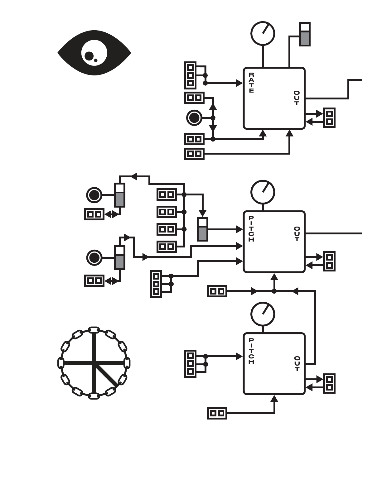
BLOCK DIAGRAM
LFO
VCO
HFO
R
A
T
E
P
I
T
C
H
SYNC
SYNC
SYNC
O
U
T
O
U
T
O
U
T
PITCH
P
I
T
C
H
PITCH
R AT E
BEND
BEND
BEND
HIGH
LOW
VCO SYNC
HFO SYNC
HARD
CLK IN
LFO CV
CONN2
CONN1
BYTE CV OUT
/CONN2
VCO CV IN
/CONN1
B Y T E
VCO CV
HFO CV
SYNC
FREEZE

CLOCK DIVIDER
MAGIC DATA PROCESSOR
R
A
T
E
P
I
T
C
H
O
U
T
O
U
T
O
U
T
P
I
T
C
H
amp
headphone out
LEFT RIGHT
DATA out
DATA
mod
/2 /32
CLK OUT
MODE
A
B
I
II
MUX 1 MUX 2
MUX1 MUX2
clk in
clk in
data in
BIT 3
OVERRIDE
/2/4/8/16/32/64
/128
/256
/512
/1024
/2048
/4096
RESET
reset
button
ancient data cave
ADVENTURE BITS
DIVIDER BITS
OVERRIDE
VOLUME
inh a b c inh a b c
BIT 5

D
IVIDER BITS
DATA
MUX1 MUX2
CLK
A
A
B
B
INH
INH
C
C
CONN 1 RESET CLK OUT O
XOR CONN 2
o+ –
LFO
LFO CV
I
II
A
B
HFO
MODE
UTILITY BELT
VOLUME
VCO
RATE
LEFT RIGHT
ADVENTURE BITS
MUX1
BIT8
BIT3
MUX2
/64
/32
/16
/8
/4
/2
/128
/256
/512
/1024
/2048
/4096
FREEZE
BEND
BEND
BEND
HARD VCO HFO
HFO CV
VERRIDE
B E
YTSYNCSYNC
IN
OVERRIDE
INSTRMNTS
CASPER ELECTRONICS
VCO CV
DIVIDER BITS
DATA
MUX1 MUX2
CLK
A
A
B
B
INH
INH
C
C
CONN 1 RESET CLK OUT O
XOR CONN 2
o+ –
LFO
LFO CV
I
II
A
B
HFO
MODE
UTILITY BELT
VOLUME
VCO
RATE
LEFT RIGHT
ADVENTURE BITS
MUX1
BIT8
BIT3
MUX2
/64
/32
/16
/8
/4
/2
/128
/256
/512
/1024
/2048
/4096
FREEZE
BEND
BEND
BEND
HARD VCO HFO
HFO CV
VERRIDE
B E
YTSYNCSYNC
IN
OVERRIDE
INSTRMNTS
CASPER ELECTRONICS
VCO CV
PAT C H

IVIDER BITS
DATA
MUX1 MUX2
CLK
A
A
B
B
INH
INH
C
C
CONN 1 RESET CLK OUT O
XOR CONN 2
o+ –
LFO
LFO CV
I
II
A
B
HFO
MODE
UTILITY BELT
VOLUME
VCO
RATE
LEFT RIGHT
ADVENTURE BITS
MUX1
BIT8
BIT3
MUX2
/64
/32
/16
/8
/4
/2
/128
/256
/512
/1024
/2048
/4096
FREEZE
BEND
BEND
BEND
HARD VCO HFO
HFO CV
VERRIDE
B E
YTSYNCSYNC
IN
OVERRIDE
INSTRMNTS
CASPER ELECTRONICS
VCO CV
DIVIDER BITS
DATA
MUX1 MUX2
CLK
A
A
B
B
INH
INH
C
C
CONN 1 RESET CLK OUT O
XOR CONN 2
o+ –
LFO
LFO CV
I
II
A
B
HFO
MODE
UTILITY BELT
VOLUME
VCO
RATE
LEFT RIGHT
ADVENTURE BITS
MUX1
BIT8
BIT3
MUX2
/64
/32
/16
/8
/4
/2
/128
/256
/512
/1024
/2048
/4096
FREEZE
BEND
BEND
BEND
HARD VCO HFO
HFO CV
VERRIDE
B E
YTSYNCSYNC
IN
OVERRIDE
INSTRMNTS
CASPER ELECTRONICS
VCO CV
TEMPLATES

10’S SOUND ALCHEMY
SYNAPSIS
CASPER ELECTRONICS
BASTL INSTRUMENTS

FEATURES
•
L
O clock oscilltor for rhythmicl
modultion
• VCO oscilltoris synced to the HFO
oscilltor
• 4 modes of opertionselectble
by 2 switches
• built in speker with volume control
• 9V DC center positive power supply
input
• 9V btterycomprtment from the
bottom
• <20mA power drwon hedphones,
<60mA with speker
(minimum 20 hours on bttery)
• On/O switch
• expnsion connector
• pckge includes 3 photo resistors –
mkeyour oscilltorsrespond to light
byplugging these into the Bend socket
PATCHBAY
• 118 jumper cble ptch points
• ech oscilltor hs 3 dierently slewed
CV inputs, sync inputs, rte knob nd
bend points
• Divider Bitssection – use clocks t
dierent speed to crete ptterns
• Adventure Bits section dds irregulr
rhythmicl elements
• MUX 1 nd MUX 2 input sections to
modulte dt loops nd wveforms
• stereophonic output from MUX 1 nd
MUX2 sections
• BYTE CV section is R2R DAC converter
which tkes bits nd converts them
to CV
• DATA modultion section witch switch
dds more vor
• Utility Belt section dds dvnced
fetures
• Left nd Right udio override section
EXTERNAL
CONNECTIVITY
• 3.5mm stereophonic hedphone
output
• Clock Input to sync the LFO oscilltor
• Clock Output with selectble LFO
division (2 or 32)
• CV Output from the BYTE DAC section
• CV Input for the VCO
• CV In nd CV Out connectors cn be
routedto dedicted ptch points on
the ptchby
ABOUT
RANGER

The bitRanger is
a patchable analog
logic computer which
sculpts sonic worlds
ranging from data noise
to melodic arpeggios.
Extensive connectivity
makes it so exible that
it can connect to almost
anything: CV control its
unique sound, sync it
with drum machines and
sequencers or use it as
an algorithmic CV/GATE
pattern generator.
THE BITRANGER
Other manuals for bitRanger
1
Table of contents


