BBK DK1010S User manual

Principle and Maintenance of DK1010S
CONTENTS
Chapter I Overview of DK1010S
1、Description of Functions
2、Block Diagram of Player
3、Composition of IC for Player
Chapter II Operating Principle of Servo Circuit
1、Processing Procedure of Digital Signal
2、Processing Procedure of Control Signal
Chapter III Operating Principle of Decoding Circuit
1、Control Circuit of System
2、Audio and Video Output Circuit
Chapter IV Operating Principle of Power Board
1、Block Diagram
2、Operating Principle of Circuits
Chapter V Operating Principle of Panel
1. Operating Principle
Chapter VI Troubleshooting
Appendix: Functions of IC Pins

Important prompt:
This type player employs two kinds of decks, SF-HD62 and SF-HD60, and
corresponding software of these two types of decks are different, therefore please
pay special attention during deck changing in the maintenance. Corresponding decks
should be changed with the same type of original ones, otherwise the player will be
out of order. Identification of decks is shown as figures:
In addition, you should also pay special attention to corresponding problem, if the
identification of the original software is ROMDAV938-0A (16M), then it should be
changed with ones of the same identification. It is the same as to software with
SF-HD62
SF-HD60

identification of ROMDK1010S-0A (16M).
This maintenance manual can be applied to player models of DK1010S, DK1020S,
DK1030S, DK1040S, DK1015S, etc.
Operating Principle Analysis ofDK1010S
Chapter I Overview of DK1010S
DK1010S is a medium-low-grade model integrating with video disc
and power amplifier, with the following major features:
1. The layer adopts “Sanyo loader+MT1389” solution;
2. The power amplifier adopts the digital power amplification circuit,
with the power IC of TAS5112DFD; it has low distortion level;
3. The audio process adopts TAS5508 , with high integration and high
performance and price ratio;
4. It has the function of radio reception, and the tuner adopts Sanzhenxing
DTS-44K(CE)module;
5. The power supply adopts the switching power, with compactness, high
efficiency and stable performance;
6. Equipped with SCART(CVBS/RGB)port;
7. Accessory channel input/output function;
8. Headphone output function;
9. Karaoke and automatic accompaniment function
10. “RDS” function;

II. Block Diagram of DK1010S Complete Player and IC Function Table:
Figure 1
Radio reception head
16M ROM
SDRAM
Sany
deck
focus
track
feed
main
load
load drive
Power Panel
status
AudioD/A,
power
Refor
Servo
drive
Digital servo
Digital signal
MPEG decoder
AV output circuit
composite
S terminal
Y/Cb/Cr
6-way
fiber,
MT1389
BA5954
4340,7265
HCU04
AT24C02
29LV160BE
Progressive
Y/Pb/Pr
VGA

III. Function Table of ICs for DK1010S
U501
0380 Switching power circuit
U502 HS817 Photo-electric coupler
U503 HA17431 2.5V reference voltage comparator
U11 LM7805 5V 3-terminal voltage-regulated
power supply
U505 0880 Switching power circuit
U506 HS817 Photo-electric coupler
Power
Board
U507 LM431 2.5V reference voltage comparator
N12 5508 Digital signal processing
N13/14 5112 Power amplification
N8/9 TLV272 Operational amplification
Amplifier
board
N10/11 RC4580 Digital signal amplification
Chapter II Operating Principle of Servo Circuit
I. Digital Signal Processing Procedure
DK1010S adopts Sanyo double beam super error correction deck and MTK decoding solution,
and its servo circuit mainly consists of preposition signal processing, digital servo processing,
digital signal processing IC MT1389 and driver circuit BA5954. MT1389 is also a main part of the
decoding circuit.
The A, B, C, D, E, F, SA, SB and RFO signal transmitted from the deck are mainly inputted
Circuit
Board No Name Function
Deck Sanyo Pick-up of disc signal
U201 MT1389 RF signal processing, digital signal
processing, servo processing, MPEG
decoding, line scan, system control
U202 AT24C02 Series EEPROM, status memory
U205 HCU04 Hex inverter
U209 LM1117MP-1.8
1.8v voltage-regulated power supply
U211 AE45164016 64Mbit SDRAM
U214 29LV160BE 16Mbit FLASH ROM
Main
Board
U302 D5954 4-channel servo driver circuit
N102 S0793 Panel control, VFD display drive
Panel N103 REMOT Remote receptor

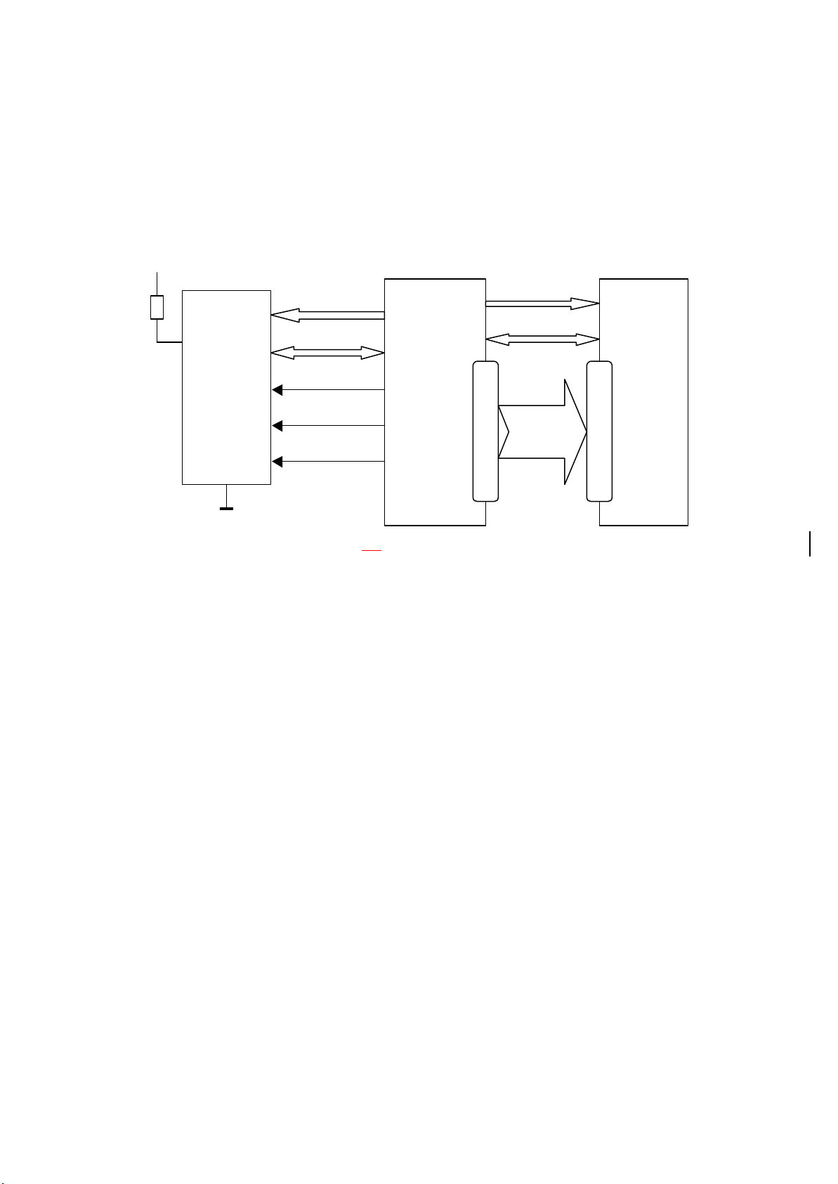
through the 2-13 pins of MT1389, and after amplifying treatment of built-in amplifier of MT 1389,
the signals are treated in two parts within MT1389:
After being processed by the internal digital servo signal circuit of MT1389, part of the signal
forms into corresponding servo control signal, and output focus (FOSO), tracking (TRSO), main
shaft (DMSO) and feed (FMSO) servo control signal from the P42, P41, P37 and P38 of MT1389
and send them to the driver circuit BA5954 to amplify the drive. After drive amplification, the
signals will drive the focus coil, tracking coil, main shaft motor and feed motor. The focus and
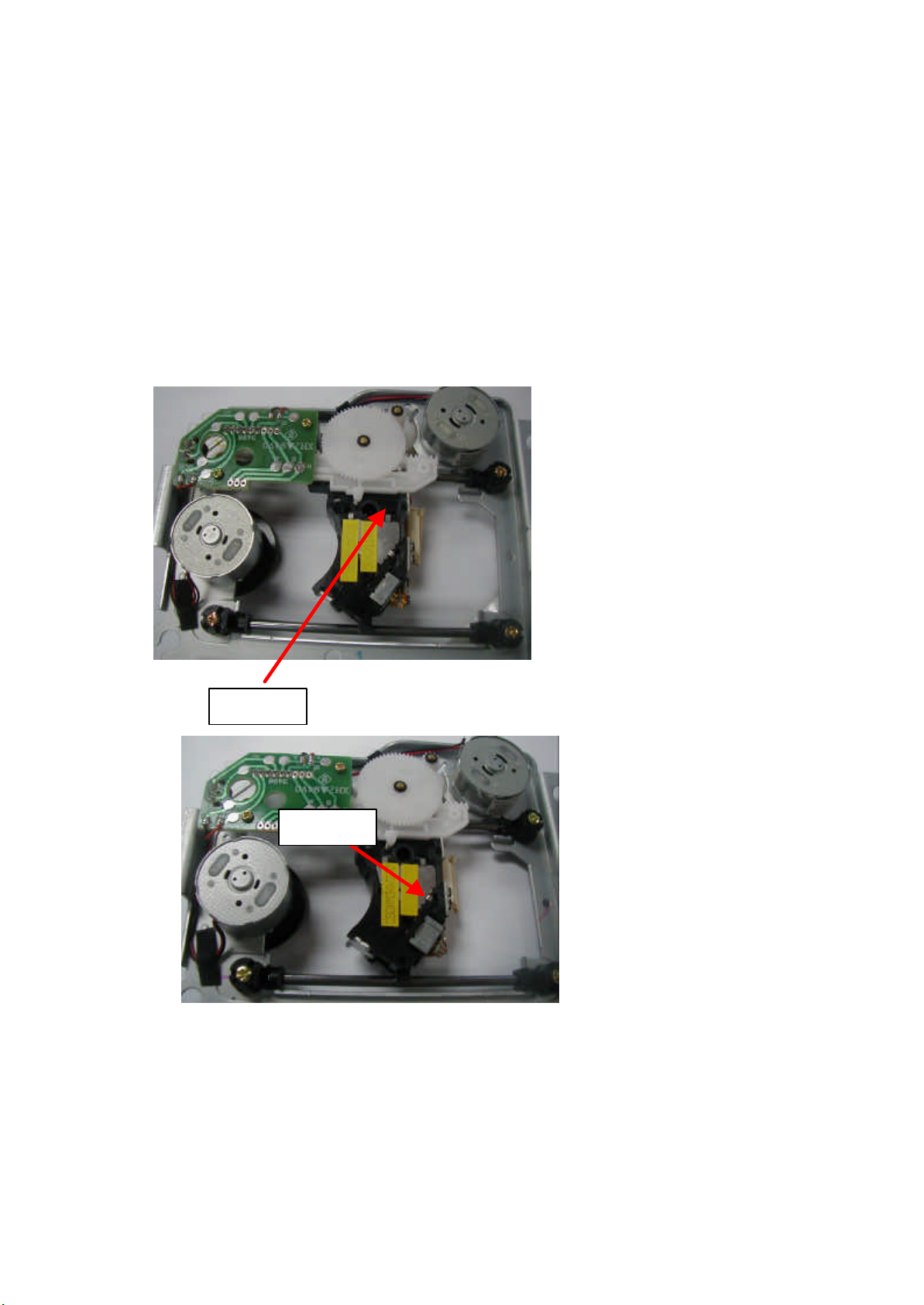
tracking servoswill be used to adjust the object lens and enable laser beam to identify signal from
compact disc correctly; the feed servo will be used to drive the laser head to move longitudinally,
and scan the compact disc; the main shaft servo is used to control the main shaft motor to read the
signals in constant linear speed and drive the disc to rotate.
After being processed by the internal VGA voltage-controlled amplifier of MT1389 in
amplification and balance frequency compensation; another part of the signals is converted into
digital signal by the internal A/D converter. When the deck readsthe CD/VCD signals, these
signals will be EFM demodulated in MT1389, and after accomplishing CIRC error regulation in
internal MT1389, output to the next grade to carry out audio and video decoding; when the deck
readsthe DVD signals, these signals will be ESM demodulated in MT1389, and after
accomplishing RSPC error regulation in internal MT1389, output to the next grade to carry out
audio and video decoding.
II. Processing Procedure of Control Signal
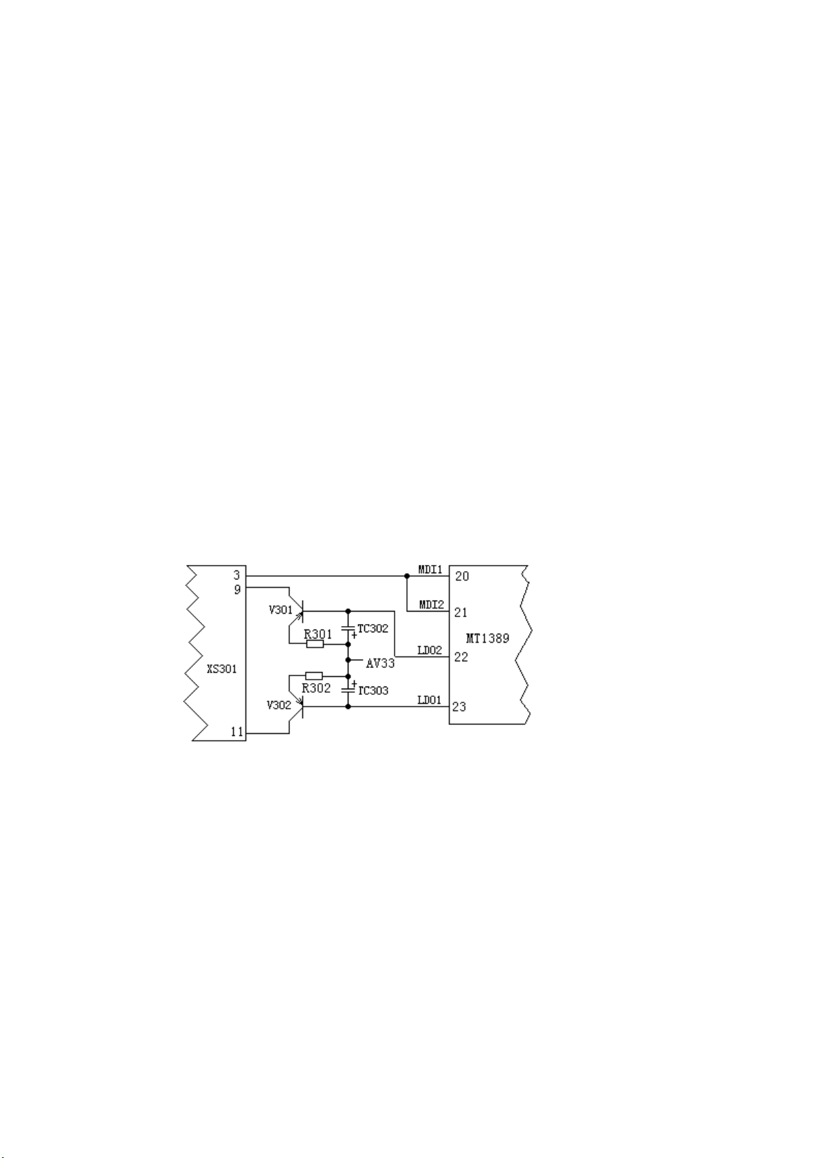
1. Automatic control of laser power, with the circuit shown as the Figure II:
Figure II
MT1389 is integrated with APC (automatic light power control) circuit. Its Pin 20 is the pin for
inputting VCD laser power rate detection signal, the Pin 21 is the pin for inputting DVD laser
power rate detection signal, and the Pin 23 is the pin for outputting VCD laser power rate drive
control. When the Pin 23 finds that the laser output power rate is too strong, the output voltage on
Pin 23 will increase after the processing of internal circuit of MT1389, and then the conduction
degree of V302 (2SB1132) and the voltage on its integration polar will decrease, which
consequently lead to the decrease of voltage supplied to the laser tube, the weakening of laser head
lighting, and thus achieve the automatic adjustment on laser output power. The Pin 22 is the pin for
outputting DVD laser power drive control, with the specific control procedure similar to that of
VCD.
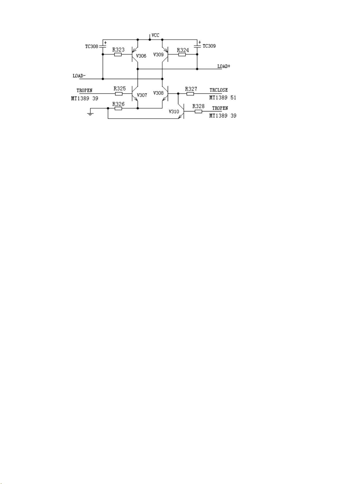
2. The tray open/close control circuit is shown as the Figure III:

Figure III
Different from the circuit in former MTK solution, the MT1389 is integrated with preposition
signal processing circuit, so the tray open/close control signals are accomplished by MT1389, that
is to say, the close control signal is accomplished by the Pin 51 of MT1389, while the open control
signal by Pin 39 of MT1389.
When we press the open button, the Pin 51 of MT1389 is in high power level, while the Pin 39 is
in low power level, and then the triode V308 will be on-state. Through resistor R323, the base of
V306 will be made to be in low power level, and V306 will be on-state, with the current direction
as the following figure:
Power voltage VCC ?V306E-C junction ?motor negative terminal
LOAD-? motor positive Load +?V308 C-E junction ?grounding
So the motor will rotate clockwise to accomplish the action of tray closing.
When we press the openbutton, the Pin 51 of MT1389 is in low power level, while the Pin 39 is in
high power level, and then the triode V307 will be conducted. Through resistor R324, the base of
V309 will be made to be in low power level, and V309 will be conducted, with the current
direction as the following figure:
Power voltage VCC ?V309E-C junction ?motor negative terminal
LOAD-? motor positive Load +?V307 C-E junction?grounding
So the motor will rotate anti-clockwise to accomplish the action of tray opening.
3. The main shaft motor braking circuit is as the Figure IV:
To prolong the lifespan of motor and reduce the influence of start-up impact current, with the
installation of disc, our R&D personnel design the main shaft motor to be in the state of constant
operation, so that even if the STOP button is pressed, the disc will not be stopped. Therefore, when
we press the OPEN button, a braking signal is required to stop the rotation of main shaft motor
immediately to accomplish the opening action in a short time.

Figure IV
During playing, if we press the OPEN button, the main shaft drive signal will disappear, and
because of inertia, the main shaft motor is still in operation. As the electromotive force generated
in the operation of motor receives the induction voltage on sampling resistors R321 and R340,
which, through the resistor R319 and R320, is added to the Pin 36 and Pin 35 of MT1389, and
outputted from the Pin 34 after internal processing for amplification in MT1389, and delivered to
Pin 47 of MT1389 through R318. After the internal A/D conversion and corresponding processing,
aninstant motor reversal braking signal will be outputted from the Pin 37 of MT1389 to stop the
rotation of main shaft motor immediately, so as to ensure the standstill of the disc when opening
the player.
III. Servo drive circuit
The servo drive of the player is accomplished through a piece of 4-channel dedicated drive circuit
BA5954, with the circuit as Figure V:
The 4 servo control signals generated in digital servo circuit processing of MT1389, i.e. focusing
control FOSO, tracking control TRSO, feed control FMSO and main shaft control DMSO signals,
are added to the pins 1, 26, 23 and 5 of BA5954 respectively, and after drive amplification of
BA5954, the focusing and tracking drive signals will be outputted from the pins 13 and 14 and
pins 15 and 16 of BA5954 respectively, and added to the focusing and tracking coils to drive the
light head to accomplish the actions of focusing and tracking.
The feed and main shaft drive signals will be outputted from the pins 17 and 18 and pins 11 and 12
of BA5954 respectively, and added to the feed motor and main shaft motor to drive the light head
to move longitudinally and enable the disc to rotate in constant linear speed.

The STBY on Pin 28 of BA5954 is an output-enabling signal, and only when the pin is in
high power level, there will be output of drive voltage on the output terminal.
Chapter III Operating Principle of Decoding Circuit
The decoding circuit of the player mainly consists of decoding chips (including MT1389, SDRAM
AE45164016 and FLASH ROM 29LV160BE) and audio DAC CS4360.
I. Control Circuit of System
1. Reset circuit is as the Figure VI:
Figure VI
The reset circuit of the player consists of triode Q204 9014, reset capacitor TC217 100uF/16V and
phase inverter U205 HCU04. In starting up, as the terminal voltage of capacitor cannot be changed
suddenly, the basic of Q204 is in low power level. After the cut-off of Q204, its emission polar is
in low power level, after secondary phase inversion by U205 and regulation, the low power level
reset signal is outputted to the Pin 110 of MT1389 to reset MT 1389.
When the recharging of TC217 is finished, the base of Q204 will be in high power level, Q204 will
be conducted, and the emission polar is in high power level. After the secondary phase inversion
and regulation by U205, a high power level is outputted and added to the Pin 110 of MT1389 to
maintain high power level during its normal operation.
2. Clock circuit
The crystal oscillator of X201 27MHz, C275/27PF, C276/27PF and phase inverter HCU04 form
into clock oscillation circuit, and the clock signals generated are added to the pins 229 and 228 of
MT1389 through R244 and 4248 to provide operating clock for MT1389.
3. Data communication circuit
The data communication circuit of the player consists of decoding chip MT1389, SDRAM,
AE45164016 and FLASH ROM 29LV160BE, as the Figure VII:
MT1389 is a piece of super large integrated circuit, with the operation voltage of +3.3V and +1.8V.
Its functions include: RF small signal preposition processing, digital servo, digital signal
processing and accomplishing MPEG decoding and video coding. The built-in MCU of MT1389 is

also the system control circuit of the whole player.
AE45164016 is a piece of 4M*16bit large capacity SDRAM, with the operation voltage of +3.3 V.
In DV971, the 6ns module is adopted, with high speed and the maximum operation frequency up
to 166MHz. Its main function is for operation buffer storage of decoding chip MT1389 to store the
audio and video data stream in decoding.
29LV160BE is a piece of 16Mbit FLASH ROM, with the operation voltage of +3.3V, mainly for
storing the user’s information including OSD character information, operational microcode and
LOGO in start-up.
II. Audio and Video Output Circuit
1. Video output circuit
DK1010S can not only output three types of alternating-line video signal (including CVBS
composite video, S terminal Y-C signal and Y/Cb/Cr color difference signal), but also output two
types of progressive line video signal (including Y/Pb/Pr progressive line color difference signal
and VGA progressive line signal).
The decoding chip MT1389 has built-in video encoding circuit for direct output of analogue
composite video signal CVBS, S terminal, color difference signal and VGA signal.
The CVBS composite video signal is outputted from the Pin 198 of MT1389, the S terminal signal
Y-C is outputted from the pins 194 and 196 of MT1389, the color difference signal and the R-B-G
signal of VGA port is outputted from the pins 203, 202 and 200 of MT1389, the row and field
synchronization signals of VGA port are outputted from the pins 207 and 205 of MT1389
respectively.
To mention specifically, the alternating-line color difference signal, the progressive line color
difference signal and progressive line R-B-G signal are outputted from the same pin, therefore the
signal output shall be selected according to the ports of TV, otherwise there will be only sound but
without picture display.
2. Audio output circuit
Audio signals processed by MT1389 output 5-track data signals through pin 217, pin 218 and pin
219 and 5-channel clock signals through pin 214 and pin 215. These signals after passing through
CLK
DQML
DQMH
CKE
113
RAS
CAS
CS
WE
BA0
BA1
15
39
38
37
18
17
19
16
20
21
137
156
157
140
139
142
138
145
143
DMA0—DMA11
DQ0—DQ15
77
A0—A21
AD0—AD7
DCE
DRD
DWR
RY/BY
BYTE
AE45164016
MT1389
29LV160BE
26
28
11
15
47
79
66
VD
GND
Figure VII

IC 74HCT125 are transmitted to audio signal processing IC TAS5508 to be processed (specific IC
data please refer to Attachment), then 10 groups of PWM signals are output, six of which are
transmitted to power amplifying parts, two of which to headphone output and two of which to
auxiliary channel output.
Six groups of signals transmitted to power amplifying IC are processed by surrounding and super
DBB sharing an N13 IC TAS5508, and by main sound channel and center sharing an N14 IC
TAS5508. Signals are amplified here, for they are digital high frequency signals, they have high
efficiency; meanwhile power IC has low colorific value. Amplified signals are still digital signals,
in order that they can be output through loudspeaker, amplified digital signals still have to be
processed before outputting.
For PWM signals containing audio signals, since high frequency signals have high frequency and
are beyond audibility range of human ears, we can ignore impacts of high frequency signals and
reduce low frequency audio signals only during processing.
TAS5508 is an 8-channel pulse width modulated high performance IC, and applicable in
processing most digital audio signals. Between 20Hz and 20KHz, it has excellent noise factor and
dynamic range. It has following features:
1、Automatically control clock speed and digital sampling speed;
2、8 groups of audio input channels;
3、8 groups of PWM output can be changed into 6-channel stereo line output or 8-channel
line output;
4、Line output is a different input open loop amplifier driven by a group of PWM signals.
IC TAS5112 is a high performance audio power amplifier. Bridging with 6O loading, each channel
can output 50W. It has 95DB dynamic range, low distortion degree and low rate of heat generation
with power efficiency up to 90%. It also has functions of low-voltage protection, high-temperature
protection, overflow protection, etc. At the same time, it has built-in driving power adjustment gate
circuit. It is applicable in family video, DVD receiver, mini music center, etc. Detailed IC
introduction see Attachment.
When in normal disc reading, digital signals and clock signals from 1389 are transmitted to pin 26
to pin 31 of IC TAS5508 through IC 74HCT125 gating. If no headphone is inserted, PH-SEL is of
high level, as well as when MUTE is normal. And pin 37 of TAS5508 is also of high level. All data
lines and clock lines can be detected by oscilloscope. One group of signals from 5508 is
transmitted to N8 and N9, then output through auxiliary channel. Another group is transmitted to
headphone; other PWM signals are transmitted to amplifying parts of amplifier.
When headphone is inserted, PH-SEL signal is forcibly shorted to earth, and turns to low level,
meanwhile amplifier is muted.
This amplifier has functions of radio reception, auxiliary channel output and karaoke. All external
inputs after N3 CD4052 gating and N7 CS5340 analog-to-digital conversion are transmitted to
MT1389. Rear processing and output is the same as the signal output flow in normal disc reading.
When in disc reading, system defaults to gate karaoke input, therefore you can open karaoke when
playing disc. This amplifier also has automatic accompaniment function, when playing VCD,
system detects external input and automatically screen to human sound signal in the disc, while
only saves sound accompaniment.
DK1010S has the function of radio reception, and can also receive RDS signal. The radio head
control lines CE, DI, CL and DO are controlled by 28 array lines connecting to MT1389 control.

When any of the controlling lines is in abnormality, the radio reception will be in malfunction. The
RDS signal received by radio head will be delivered to the dedicated IC SAA6588 for processing.
Chapter IV Operating Principle of Power Board
I. Block Diagram
This amplifier has two groups of power supply; one is of low voltage for decoding board and low
power ICS, the other is of higher voltage for power amplifying IC. But their design principles, we
only draw one functional block diagram of them:
II. Introduction of Circuit Principle
220V alternating current is loaded on D501-D504 integrated bridging rectification circuit through
power plug, fuse tube, voltage dependent resistor R501 and common mode rejection BC501 and
L501. Diode adopts IN4007 which ahs better PPR and higher withstand voltage value than IN4001.
Output 311V direct current after being bridging rectified is loaded on two transformers through
TC501 filtering and transmitted to DRAIN control pins of switch modules U501 and U502.
Service voltage of power on IC after being directly rectified and filtered is divided by resistors to
serve IC. Diode D508, capacitor C516 and resistor R516 form absorption circuit to provide
discharge circuit of reverse electromotive force for 1-4 coils of transformers. Pin FB controlling IC
is feedback control pin, so you should decide on/off time of pulse width according to current
intensity on it to ensure stability of output voltage.
There are 5 branch circuits coupled to sub-grade through transformer.
1. Voltage output from pin 11 and pin 13 of transformer T501 outputs a group of +28V voltage
for power amplifying IC after being rectified and filtered.
2. Voltage output from pin 16 of transformer T501 outputs a group of +12V voltage after being
rectified and filtered. +12V voltage is stabilized into a group of +5V voltage by IC LM7805.
3. Voltage output from pin 14 of transformer T501 outputs +5V voltage and provide voltage for
one end of photo-electric coupler U502 after being rectified and filtered.
4. Voltage output from pin 12 of transformer T501 outputs +3.3V voltage and provide a group of
stable voltage for CPU after being rectified and filtered.
5. Voltage output from pin 9 of transformer T501 outputs a group of 21V voltage for displaying
driving IC after being rectified and filtered. Clamp ZD501 of -21V provide heater voltage for
panel display screen. Grounding direct voltage of FL+ and FL-is about -16V.
Operating principles of two groups of switch power are the same, therefore we will only analyze
the group providing +3.3V voltage for CPU here:
Feedback sampling of this group comes from 3.3V and supplies for photocupler HS817 through
D516 and R506. At the same time, it is divided through R508 and R509 for reference voltage pin R
of 2.5V comparator. When 3.3V becomes higher, pin KA of comparator is on; and the voltage is
transmitted to pin 4 of switch IC 5L0380R after photoelectric coupling through HS817 to reduce
on time of internal switch tube. And thus it reduces transformer coupling and decreases output of
3.3V voltage to achieve automatic adjustment and control, and vice verse.
It has to be noted that in this switching power reference voltage comparator IC of two groups of
switching power are different. For voltage of the group supplying power for amplifier is higher, it
adopts LM431 which has better performance and higher withstand voltage. And voltage of the

group supplying power for 3.3V is lower, it adopts 17431. For two ICs are different, you should
pay special attention to distinguish them from each other. They cannot be used mixing.
Chapter 5: Panel control and VFD display circuit
The panel mainly consists of VFD screen, driver IC0793, remote receptor HS0038A2 and
button and indicator display circuit, mainly for accomplishing man-player dialogue and display of
operation status.
The structural drawing is as follows:
Figure XI
MT1389 will control the U401 IC 0793 to display the operation status of the player through the
VFDST status, VFDCK clock and VFDAT data, under the control of CPU built in MT1389,
receive the user control commands sent by UPD16312, and control the controlled circuit of the
player to limit the player to operate in specified status.
When the user operatesthe panel buttons, the control command is sent to the IC 0793 through
keyboard-scanning circuit, and through internal decoding drive, the IC 0793 outputs the control
data from the pins 5 and 6 (VFDAT) to the built-in CPU of MT1389, which will realize the control
on the controlled circuit, and control the VFD through IC 0793.
VFD401 is a vacuum fluorescence screen, and its biggest feature is its high brightness.
Its operation principle is similar to the kinescope of TV. The pins 1, 2, 34 and 35 are for filament
power supply; the pins 27-32 are GRID poles, each GRID has 16 different characters of display;
the pins 4-19 are SEG poles, and the CPU control the SEG poles through its control on IC 0793,
and display the characters of corresponding operation status on the screen.
The remote reception circuit mainly consists of remote receptors HS0038A2, of which the pin 1 is
for grounding, the pin 2 for power supply, the pin 3 for output of reception signal, and they are all
connected directly to the CPU in MT1389 to control the corresponding circuit.
This player has headphone output function. A pin in the headphone directly connects to TAS5508. When the
headphone is inserted, detection line H-DET grounds and turns into low level. When pin 12 of TAS5508 turns
U401
IC 079
3
VFD
display
Keystroke
control
U201
MT1389
Remote
receiving
Panel indicator control
VFDST
VFDCK
VFDAT

into low level, parts of output of amplifier are muted. When in normal condition, this detection pin is of high
level around 3.3V.
Troubleshooting
I. Voltage on key points of DK1010S
Demoding circuit:
Reset:
1. U205 (HCU04): 8 pins, around 5V;
2. MT1389: 110 pins, around 5V;
3. FLAHS ROM: 12 pins, around 5V
Clock:
27MHZ crystal oscillator two ends: Around 0.77V.
I2C bus SDA: 3.3V
I2C bus SCL 3.3V
Servo circuit:
LD01:3.3V;LD02:3.3V
V301 and V302 electron collector LD voltage: 2.3V
BA5954 pin 4 base voltage: 1.4V
BA5954 pins 15 and 16 tracking drive output: Around 2.5V
BA5954 pins 17 and 18 feed drive output: Around 2.5V
BA5954 pins 13 and 14 focus drive signal output: Around 2.5V
BA5954 pins 11 and 12 main shaft drive output: Around 2.5V
BA5954 pin 1 focus control signal input: 1.4V
BA5954 pin 5 main shaft control signal input: 1.4V
BA5954 pin 26 tracking control signal input: 1.4V
BA5954 pin 23 feed control signal input: 1.4V
Amplifier circuit:
TAS5508 pin 9 power supply pin 3.3V
TAS5112 32、33、40、41、44、45、52、53, 28V。\

II. Troubleshooting of main troubles
NO
YES
NO
YES
NO
YES
No
picture,no sound, no VFD
display
Check if power supply of MT1389
3.3V, 1.8V is right?
Check the voltage of power board,
and check if the decoding board
is
short circuit to the grounding.
If the clock signal output XO
and XI is right?
Check if clock oscillating circuit
27M crystal oscillator
, C275,
C276, R224, R248 are damaged?
Check if reset signal URST#
is
in 5V high level?
Check if the reset circuit which is
comprised by HCU04 and
Q204 etc.
is in working order?
Check if I2C bus,
SDA, SCL 3.3V
voltage is right?
Check if the AT24C16, CS4360,
MT1389 SDA and SCL are
short
circuit to grounding, if R259 and
R260
are in working order?
Check i
f SDRAM CLK, CS, RAS, CAS,
WE communication signalsare right?Check i
f FLASH ROM, URST, DCE,
DRD, DWR signalsare right?
Check if the connection between
MT1389, FLASH, SDRAM is right?
Check if the MT1389, SDRAM and
FLASH are damaged?

NO
YES
YES
YES
NO
NO
YES
YES
YES NO
Do not read disc
Check if the
laser
head has feed action.
Check if the
feed control
input of BA5954 Pin
23 is
1.4V?
Check if BA5954 pin
17,18
have 2.5V voltage output?
Check if BA5854 and the pow
er
supply 5V are in working order?
Check if the
connection from
BA5954 to MT1389
is open circuit?
Check feed motor
and its connection.
Check if laser head
has focus action?
Check if BA5954 pin 1
has focus
control
voltage input of1.4V.
Check if the
connection from
BA5954 to MT1389
is open circuit?
Check if the
voltage output of
BA5954 pin 13 and 14 a
re
2.5V?
Check focus
coil and its
connection.
Check if BA5854 and 5V power
supply are in working order?

NO
YES
YES YES
NO
YES
YES
YES
NO
Check if there is
laser coming out
from laser head?
Check if the signal
voltage of LD01, LD02
is 3.2V?
Check MT1389 and its
connection.
Check if V
301 and V302
electron collector voltage is
2.3V?
Check if the laser head
and its array line are
right?
Check if the
main shaft
rotates?
Check if the control
voltage of BA5954 pin
5
main shaft is 1.4V?
Check if the connection from
BA5954 to MT1389 is op
en
circuit?
Check if BA5954 or
main shaft
motor is damaged?
Check if BA5954 pin
11
and 12 output is 2.5V?
Check if MT1389
and its
peripheral
circuit is right?
Check if BA5854 and 5V power
supply are in working order?

Attachment :Brief Introduction to IC Pins
I. MT1389
MT1389 adopts the LQFP 256 pin packaging and 3.3V/1.8V double voltage operation mode. It is a
piece of large-scale CD-ROM and DVD-ROM preposition processing CMOS integrated circuit
with excellent performance, and a single chip dedicated to CD/VCD/DVD player. It contains
focusing servo error amplification, tracking servo error amplification and RF level output servo
control, including the following main functions:
RF small signal preposition processing, mainly for carrying our corresponding processing and
amplification on the RF signalstransmitted from the light head part, adjusting the laser output
power automatically, and identifying the VCD disc and DVD disc.
Digital servo processing can generatefocusing, tracking, feed and main shaft servo control signals;
digital signal processing, accomplishing the EFM/EFM + demodulating of RF signals.
MPEG-1/MPEG-2/MPEG4/JPEG Video decoding chip, which can not only realize the decoding of
VCD and DVD, but also realize MPEG 4 network video decoding, being compatible to “network
movie” disc, and decipher JPED pictures to realize the function of digital photo album play.
On audio aspect, it can not only realize AC-3/DTS double decoding, decipher MP3, and is
also compatible to DVD-Audio decoding to achieve high-resolution sound restoration in 1000
times higher thanCD.
By utilizing the 8032 microprocessor with built-in chip, MT1369E can also realize the system
control function of player, which simplifies the circuit design substantially.
The pin functions of MT1389 are as the following table:
Pin Name Function
1 AGND Analogue grounding
2 DVDA DVD-RF high-frequency AC coupling
signal A
3 DVDB DVD-RF high-frequency AC coupling
signal B
4 DVDC DVD-RF high-frequency AC coupling
signal C
5 DVDD DVD-RF high-frequency AC coupling
signal D
6 DVDRFIP DVD-RF high-frequency AC coupling
signal RFIP input
7 DVDRFIN DVD-RF high-frequency AC coupling
signal RFIN input
8 MA DVD-RAM main light beam RF DC
signal input A

9 MB DVD-RAM main light beam RF DC
signal input B
10 MC DVD-RAM main light beam RF DC
signal input C
11 MD DVD-RAM main light beam RF DC
signal input D
12 SA DVD-RAM auxiliary light beam RF DC
signal input A
13 SB DVD-RAM auxiliary light beam RF DC
signal input B
14 SC DVD-RAM auxiliary light beam RF DC
signal input C
15 SD DVD-RAM auxiliary light beam RF DC
signal input D
16 CDFON CD focusing error phase inversion input
17 CDFOP CD focusing error phase input
18 TNI 3 light beam auxiliary PD signal phase
inversion input
19 TPI 4 light beam auxiliary PD signal phase
input
20 MDI1 Laser power monitoring input 1
21 MDI2 Laser power monitoring input 2
22 LDO2 Laser power monitoring output 2
23 LDO1 Laser power monitoring output 1
24 SVDD3 Servo 3.3V power supply
25 CSO/RFOP Main servo signal output/RF phase
output
26 RFLVL/RFON RF level output/RF phase inversion
output
27 SGND Servo grounding
28 V2REFO Reference voltage 2.8V
29 V20 Reference voltage 2.0V
30 VREFO Reference voltage 1.4V
31 FEO Focusing error signal output
32 TEO Tracking error signal output

33 TEZISLV Tracking zero crossover error input
34 OP_OUT Sensing signal amplification output
35 OP_INN Sensing signal phase inversion input
36 OP_INP Sensing signal non-inverting input
37 DMO Main shaft control signal output
38 FMO Feed control signal output
39 TROPEN PWM Tray Open signal output
40 PWMOUT1/ADIN9
First-route pulse width demodulating
signal output/AD universal input
41 TRO Tracking control signal output
42 FOO Focusing control signal output
43 USB_VSS USB grounding
44 USBP USB data
45 USBM USB data
46 USB_VDD3 USB 3.3V power supply
47 FG/ADIN8 Motor sensing signal input/AD universal
input
48 TDI/ADIN4 Open position detecting signal input/AD
universal input
49 TMS/ADIN5 Close position detecting signal input/AD
universal input
50 TCK/ADIN6 BA5954 enabling signal output/AD
universal output
51 TDO/ADIN7 Tray close signal output/AD universal
input
52、97、122、
152、173、221
DVDD18 Digital 1.8V power supply
53-58 IOA2-7 Micro-controller address bit 2-7
59 HIGHA0 Micro-controller address bit 0
60、61 IOA18-19 Micro-controller address 18-19
62、85、94、116、
119、134、144、
148、161、163、
175、216、223
DVSS Digital grounding
63 APLLCAP Analogue phase lock loop external
capacitor
Table of contents
Other BBK Home Theater System manuals