BBK ABS730X User manual

SERVICE MANUAL
ABS730X

CONTENTS
1. SAFETY PRECAUTIONS 1
2. PREVENTION OF ELECTRO STATIC DISCHARGE(ESD)TO ELECTROSTATICALLY
SENSITIVE(ES)DEVICES 1
4. PREVERTION OF STATIC ELECTRICITY DISCHARGE 3
5. ASSEMBLING AND DISASSEMBLING THE MECHANISM UNIT 4
5.1 OPTICAL PICKUP UNIT EXPLOSED VIEW AND PART LIST 5
6. ELECTRICAL CONFIRMATION 6
6.1 VIDEO OUTPUT (LUMINANCE SIGNAL) CONFIRMATION 6
6.2 VIDEO OUTPUT(CHROMINANCE SIGNAL) CONFIRMATION 7
8
8. SCHEMATIC & PCB WIRING DIAGRAM 11
9. SPARE PARTS LIST 35
7. AML3298
3. CONTROL BUTTON LOCATIONS AND EXPLANATIONS 2
5.2 MISCELLANEOUS 5

1.1 GENERAL GUIDELINES
1. When servicing, observe the original lead dress. if a short circuit is found, replace all parts which have
been overheated or damaged by the short circuit.
2. After servicing, see to it that all the protective devices such as insulation barrier, insulation papers
shields are properly installed.
3. After servicing, make the following leakage current checks to prevent the customer from being exposed
to shock hazards.
Some semiconductor(solid state)devices can be damaged easily by static electricity. Such components
commonly are called Electrostatically Sensitive(ES)Devices. Examples of typical ES devices are integrated
circuits and some field-effect transistors and semiconductor chip components. The following techniques
should be used to help reduce the incidence of component damage caused by electro static discharge(ESD).
1. Immediately before handling any semiconductor component or semiconductor-equipped assembly, drain
off any ESD on your body by touching a known earth ground. Alternatively, obtain and wear a commercially
availabel discharging ESD wrist strap, which should be removed for potential shock reasons prior to
applying power to the unit under test.
2. After removing an electrical assembly equipped with ES devices,place the assembly on a conductive
surface such as alminum foil, to prevent electrostatic charge buildup or exposure of the assembly.
3. Use only a grounded-tip soldering iron to solder or unsolder ES devices.
4. Use only an anti-static solder removal device. Some solder removal devices not classified as anti-static
(ESD protected)can generate electrical charge sufficient to damage ES devices.
5. Do not use freon-propelled chemicals. These can generate electrical charges sufficient to damage ES
devices.
6. Do not remove a replacement ES device from its protective package until immediately before you are
ready to install it.(Most replacement ES devices are packaged with leads electrically shorted together by
conductive foam, alminum foil or comparable conductive material).
7. Immediately before removing the protective material from the leads of a replacement ES device, touch
the protective material to the chassis or circuit assembly into which the device will be installed.
Caution
Be sure no power is applied to the chassis or circuit, and observe all other safety precautions.
8. Minimize bodily motions when handling unpackaged replacement ES devices. (Otherwise harmless motion
such as the brushing together of your clothes fabric or the lifting of your foot from a carpeted floor can
generate static electricity(ESD).
notice (1885x323x2 tiff)

BAND switch
6
5SKIP knob
8
AUDIO IN 1 button
4
2Headphone jack
Echo button
OPEN/CLOSE button
TONE button
VOL +/- button
EQ button
SF button
TIMER button
CLOCK button
MIC 1 jack
3Audio in 1
7
MIC 2 jack
AUDIO IN 2 button
10
PSM button
Power switch
12 22
16 26
11 21
15 25
9
13 23
17 27
19 29
IR sensor
FW
D button
STOP button
PLAY button
PAUSE button
REW button
TUNER button
TUNING+ -
SAVE button
DVD button
Number buttons
MIC VOL knob
14 24
18 28
20 30
Control Button Locations and Explanations
Front Panel Illustration 1
1
2
3
4
5
6
7
8
9
10
11
12 13 14 15 16
17
18
19
20
21
22
23
24
252627282930

The laser diode in the traverse unit (optical pickup)may brake down due to static electricity of clothes or human
body.Use due caution to electrostatic breakdown when servicing and handling the laser diode.
4.1.Grounding for electrostatic breakdown prevention
Some devices such as the DVD player use the optical pickup(laser diode)and the optical pickup will be damaged
by static electricity in the working environment.Proceed servicing works under the working environment where
grounding works is completed.
4.1.1. Worktable grounding
1. Put a conductive material(sheet)or iron sheet on the area where the optical pickup is placed,and ground the
4.1.2.Human body grounding
1 Use the anti-static wrist strap to discharge the static electricity from your body.
4.1.3.Handling of optical pickup
1. To keep the good quality of the optical pickup maintenance parts during transportation and before
installation, the both ends of the laser diode are short-circuited.After replacing the parts with new ones,
remove the short circuit according to the correct procedure. (See this Technical Guide).
2. Do not use a tester to check the laser diode for the optical pickup .Failure to do so willdamage the laser
diode due to the power supply in the tester.
4.2. Handling precautions for Traverse Unit (Optical Pickup)
1. Do not give a considerable shock to the traverse unit(optical pickup)as it has an extremely high-precise
structure.
2. When replacing the optical pickup, install the flexible cable and cut is short land with a nipper. See the
optical pickup replacement procedure in this Technical Guide. Before replacing the traverse unit, remove
the short pin for preventingstatic electricity and install a new unit.Connect the connector as short times as
possible.
3. The flexible cable may be cut off if an excessive force is applied to it.Use caution when handling the cable.
4. The half-fixed resistor for laser power adjustment cannot be adjusted. Do not turn the resistor.
safety_3 (1577x409x2 tiff)
sheet.

1
2
3
4
5
6
7
8
9
10
11
12
13
14
15
16
19
18
17
20
21
22
23
24
25
10
26
27
30
31
32
33
34
35
37
38
39
43
42
41
40
28
29
5.1 Optical pickup unit explosed view and partlist
1 Upper cover
2 Power amplifier PCB
3 Left bracket of heat radiator
4 Backing plate
5 Display PCB
6 Front panel PCB
7 Left function button
8 Number button
9 PCB bracket
10 Bracket of upper casing
11 Surface casing
12 Display glass
13 Left function button
14 Upper decorative board
15 Door
16 Lower decorative board
17 Knob cover
18 Volume knob
19 Light conduct ring
20 Power button
21 MIC PCB
22 Open button
23 Cap of function button
24 Decorative button
25 5-direction function button
26 Right function knob
27 4-direction function button
28 Right bracket of heat radiator
29 Loader
30 Decode board
31 Bottom board
32 Power board
33 Loader bracket
34 Rear bracket of heat radiator
35 Cover for ventilation of heat radiator
36 Power cord
37 Rear board
38 Tuner
39 Output board
40 Heat radiator
41 IC press plate
42 Supplementary power board
43 Power amplifier PCB bracket
36

5.2 MISCELLANEOUS
5.2.1 Protection of the LD(Laser diode)
Short the parts of LD circuit pattern by soldering.
5.2.2 Cautions on assembly and adjustment
Make sure that the workbenches,jigs,tips,tips of soldering irons and measuring instruments are
grounded,and that personnel wear wrist straps for ground.
Open the LD shortlands quickly with a soldering ironafter a circuit isconnected.
Keep the power source of the pick-up protected from internal and external sources of electrical
noise.
Refrain from operation and storage in atmospheres containing corrosive gases (such as H2S,SO2,
NO2 and Cl2)or toxic gases or in locations containing substances(especially from the organic silicon,cyan,
formalin and phenol groups)which emit toxic gases.It is particularly important to ensure that none of the
above substances are present inside the unit.Otherwise,the motor may no longer run.

6.1. Video Output (Luminance Signal) Confirmation
DO this confirmation after replacing a P.C.B.
Purpose:To maintain video signal output compatibility.
1.Connect the oscilloscope to the video output terminal and terminate at 75 ohms.
2.Confirm that luminance signal(Y+S)level is 1000mVp-p±30mV
Measurement point
Video output terminal
Color bar 75%
PLAY(Title 46):DVDT-S15
PLAY(Title 12):DVDT-S01
DVDT-S15
or
DVDT-S01
Mode Disc
Measuring equipment,tools
200mV/dir,10 sec/dir 1000mVp-p±30mV
Confirmation value

Do the confirmation after replacing P.C.B.
Purpose:To maintain video signal output compatibility.
1.Connect the oscilloscope to the video output terminal and terminate at 75 ohme.
2.Confirm that the chrominance signal(C)level is 621 mVp-p±30mV
Measurement point
Video output terminal
Color bar 75%
PLAY(Title 46):DVDT-S15
PLAY(Title 12):DVDT-S01
DVDT-S15
or
DVDT-S01
Mode Disc
Measuring equipment,tools Confirmation value
Screwdriver,Oscilloscope
200mV/dir,10 sec/dir 621mVp-p±30mV

Amlogic, Inc.CompanyConfidential8
1 Overview
The AML3298 A/V processor is a completely integrated system targeting all types of Audio/Video decoder
applications that provide connectivity to hard disk, digital camera, MP3 players and other external digital
consumer devices. The target market for AML3298 A/V processor is feature rich DVD players, audio receivers,
DVD/receiver combo players, digital media players, portable DVD players, and portable media players.
The AML3298 combines full function of MPEG-1, MPEG-2 and MPEG-4 decoding, numerous dedicated and
general-purpose peripherals, and a high speed 32-bit host CPU in a single device. The AML3298 has two built-in
AMRISCTM RISC processors with special instructions to accommodate audio and video digital signal processing.
The AML3298 also provides a high speed interface to external USB 1.1/2.0 chip for connectivity to popular USB
devices like hard disk, Flash memory, digital camera and MP3 players.
The embedded 32-bits host CPU handles system initialization, DVD navigation, and other system applications.
The AML3298 A/V processor provides a glueless interface to all external components: ATAPI loaders, USB
interface chip, audio DACs and memory. Numerous general-purpose I/O pins can be used to control the front
panel display and other miscellaneous tasks. The Flash interface allows the Flash memory to be shared with the
front-end chip to reduce system cost in mono-board designs. Together, the embedded host CPU and special
glueless interfaces reduce the total system cost for all A/V applications from any media.
The AML3298 A/V processor also integrates an NTSC/PAL TV encoder that supports S-Video, composite, YUV
component and RGB. The video encoder also supports high-quality de-interlaced progressive scan (480p/576p)
with full Macrovision support. Contrast enhancement, hue adjustment, video scaling, video interpolation, pan-
scan, letter-box, and zoom are also supported. In addition, four built in video DACs complement the video
encoder further reducing system cost. In addition, the AML3288 devices can also provide CCIR601 and VGA
video output.
The integrated AMRISCTM RISC processor is designed to support advanced digital audio processing. The micro-
coded engine provides support for all existing audio formats and it also has enough flexibility to accommodate
new audio standards. Popular audio formats like Dolby AC-3 5.1, HDCD, MP-3 and WMA are supported. In
addition, SPDIF (IEC958) input and outputs are supported.
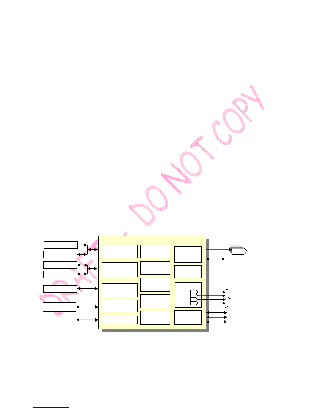
Figure 1 AML3298 Block Diagram
Audio
DACs
S-Video
CVBS
Component
Progressive
RGB
SPDIF (IEC958)
Video
Scaling
& Conversion
32-bit CPU
Audio
Interface
Video
DRAM Controller
JTAG
GPIO
Flash Controller /
USB DMA Engine
ADATA
UART
UART_RX
UART_TX
Video
AMRISC
AML3298 A/V Processor
Audio
AMRISC
ATAPI / HDD
interface
FLASH
SDRAM
Audio
Decoder
Video Decoder
Enhancement
Audio/Video
Stream Praser
VD [7:0]
NGP[5:0]
IIS[7:0]
USB 1.1/2.0
DVD-ROM
IDE HDD

Amlogic, Inc.CompanyConfidential9
2 Features
MPEG 1/2/4 Decoding
-MPEG-4 and Divx 3.x/4.x/5.x complaint
-MPEG-2 ML/MP conforming to ISO-13818
-MPEG-1 ML/MP conforming to ISO-11172
-On-chip CSS descrambler
-Flexible DRM engine for content management
-Compliant with DVD Specification 1.0 for read-only Disc
decoding
-Advanced error detection, concealment, and recovery
scheme
-Backward compatible VCD (1.0 - 2.0) decoding
-Super VCD decoding
-Built-in AMRISCTM 24-bit 133 MHz RISC CPU with special
instruction extensions designed specifically for MPEG
decoding
Video
-Full MPEG-2 main profile @ main level 4:2:0 video
decoding
-Advanced pixel based de-interlacing algorithm
-On-Screen-Display (OSD) capable of supporting up to 256
prefixed colors or 16 programmable colors
-OSD Alpha-blending over video display
-Automatic scaling of sub-standard size DivX clips
-Video Zoom in for visual effects
-Built-in full screen NTSC to PAL scaling or vice-versa
-Built-in contrast enhancement and hue adjustment
-Built-in hardware for video interpolation and decimation
-Supports maximum zoom ratio up to 8X
Graphics
-Anti-flicker hardware for interlaced video
-Supports high speed block move for panning
-Built-in 2D graphics accelerator
-Dedicated graphics display controller separate from MPEG
engine for optimal video overlay performance
-Supports NTSC and PAL graphics modes with maximum
64K color
-Video overlay with graphics and vice-versa
-Unified MPEG and graphics memory architecture for
maximum flexibility and system cost savings
Built-in TV encoder
-Quad 10-bit video DACs
-Real-time Interlaced NTSC output 720x480 at 30 fps and
PAL 720x576 at 25 fps. Macrovision 7.1L1 anti-taping
process
-NTSC Progressive output (480p) at 60fps, PAL Progressive
(576p) at 50fps. Macrovision 1.03 anti-taping process
-Interlaced: S-Video, component, composite and SCART
output
-Close caption
- Progressive RGB
Audio
-Built-in AMRISCTM RISC CPU with extensions specifically
designed for Audio Processing
-Compliant with Dolby AC-3 5.1 channel decoding
-AC-3 two channel down-mixing
-SPDIF (IEC958) input and output
-Full MPEG audio layers I, II and III (MP3)
-Supports 8 channel linear PCM output
-DTS, HDCD, MP3 and WMA
Built-in Host CPU
-133Mhz 32-bit CPU dedicated for user applications
-Embedded debug interface using ICE/JTAG
-Able to utilize MPEG SDRAM as run time data storage for
minimal system cost
-Configurable for 16-bit wide SDRAM
-Support 8 or 16-bit FLASH
- FLASH memory can be shared with Front-End chips
Peripherals and Interface
-High speed (DMA) direct connection to third party USB chip
-Supports glueless interface to DVD DSP, CD DSP, and
DVD-ROM devices
-Direct connection to Audio DACs using I2S
-General Purpose I/O pins
-IDE with DMA transfer supporting up to 2 IDE devices such
as ATAPI DVD-ROM and IDE hard disk
-ISA interface
Miscellaneous
-208-pin PQFP
-1.8V operating voltage, 5V tolerant inputs, 3.3V output

AML3298 A/V Connectivity Processor
Amlogic, Inc.CompanyConfidential10
3 AML3298 – 208 Pin Package Diagram
156
155
154
153
152
151
150
149
148
147
146
145
144
143
142
141
140
139
138
137
136
135
134
133
132
131
130
129
128
127
126
125
124
123
122
121
120
119
118
117
116
115
114
113
112
111
110
109
108
107
106
105
208
207
206
205
204
203
202
201
200
199
198
197
196
195
194
193
192
191
190
189
188
187
186
185
184
183
182
181
180
179
178
177
176
175
174
173
172
171
170
169
168
167
166
165
164
163
162
161
160
159
158
157
53
54
55
56
57
58
59
60
61
62
63
64
65
66
67
68
69
70
71
72
73
74
75
76
77
78
79
80
81
82
83
84
85
86
87
88
89
90
91
92
93
94
95
96
97
98
99
100
101
102
103
1
04
1
2
3
4
5
6
7
8
9
10
11
12
13
14
15
16
17
18
19
20
21
22
23
24
25
26
27
28
29
30
31
32
33
34
35
36
37
38
39
40
41
42
43
44
45
46
47
48
49
50
51
52
AOCLK
ADATA
_2
ADATA
_3
IEC
958
IIS
_0
IIS
_1
IIS
_2
IIS
_3
IIS
_4
IIS
_5
IIS
_6
IIS
_7
DD
_12
DD
_11
DD
_10
DD
_9
DD
_8
DD
_7
DD
_6
DD
_5
DD
_4
VDD
_1.8
V
VSS
_1.8
V
VSS
_3.3
V
VDD
_3.3
V
DD
_3
D
D
_2
DD
_1
DD
_0
DMACK
_
N
DIOW
_
N
DIOR
_
N
CS
0_
N
CS
1_
N
DMARQ
CSEL
TDO
RESET
_
N
TEST
_
N
TRST
_
N
TCK
TDI
T
MS
AICLK
_
XOUT
AICLK
_
XIN
SCLK
_
XOU
T
SCLK
_
XIN
DVDD
_
PLL
1
VSS
_
PLL
1
A
VDD
_
PLL
1
DVDD
_
PLL
0
DVSS
_
PLL
0
ADATA_1
ADATA_0
ALRCLK
VSS_3.3V
AMCLK
VDD_3.3V
DD_13
DD_14
DD_15
DA_0
DA_1
DA_2
VSS_1.8V
VDD_1.8V
NGP_5
NGP_4
IVDD_DAC1(1.8V)
VSS_DAC1(1,8V)
IOX
AVDD
_DAC1_X (3.3V)
AVSS
_DAC1_X (3.3V)
IOB
AVDD
_DAC1_B (3.3V)
AVSS
-DAC1_B (3.3V)
IOG
AVDD
-DAC1_G (3.3V)
AVSS
-DAC1_G (3.3V)
IOR
AVDD
_DAC1_R (3.3V)
AVSS
_DAC1_R (3.3V)
COMP1
RSET1
VREF1_OUT
VREF1_IN
AVSS
_DAC1(3.3V)
AVDD
_DAC1(3.3V)
NGP_3
NGP_2
NGP_1
VDD_1.8V
VSS_1.8V
M2_CLKO
M2_DQM1
M2_BA1
M2_BA0
M2_SCS_N
VSS_3.3V
VDD_3.3V
UART_RX
UART_TX
NGP_0
VD_7
AVSS_PLL0
AVDD_PLL0
VDD_3.3V
VSS_3.3V
M1_A_3
M1_A_2
M1_A_1
M1_A_0
M1_A_10
M1_A_11
M1_BA1
M1_BA0
M1_SCS_N
M1_RAS_N
M1_CAS_N
VDD_3.3V
VDD_1.8V
VSS_1.8V
DIORDY
IRQ14
VSS_3.3V
M2_D_15
M2_D_1
M2_D_2
M2_D_3
M2_D_4
M2_D_5
M2_D_6
M2_D_0
M2_D_7
M2_A_0
M2_A_1
M2_A_10
VDD_3.3V
VSS_3.3V
M2_A_2
M2_A_3
M2_A_4
M2_EOE_N
M1_EOE_N
M1_WE_N
M1_A_4
M1_A_5
M1_A_6
M1_A_7
M1_A_8
M1_A_9
VDD_1.8V
VSS_1.8V
M1_CLKO
VDD_3.3V
VSS_3.3V
VD
_6
VD
_5
VD
_4
VD
_3
VD
_2
VD
_1
VD
_0
VSS
_3.3
V
VDD
_3.3
V
M
2_
A
_5
M
2_
A
_9
M
2_
A
_11
M
2_
RAS
_
N
M
2_
CAS
_
N
M
2_
DQM
0
M
2_
D
_8
M
2_
D
_11
M
2_
D
_12
M
2_
D
_14
M
2_
WE
_
N
VSS
_3.3
V
VDD
_3.3
V
M
2_
D
_13
M
2_
D
_10
M
2_
A
_7
M
2_
D
_9
M
2_
A
_6
M
2_
A
_8
M
2_
ECS
_
N
VSS
_1.8
V
VDD
_1.8
V
M
1_
ECS
_
N
M
1_
D
_0
M
1_
D
_1
M
1_
D
_2
M
1_
D
_3
M
1_
D
_4
M
1_
D
_5
VSS
_3.3
V
VDD
_3.3
V
M
1_
D
_6
M
1_
D
_7
M
1_
D
_15
M
1_
D
_14
M
1_
D
_13
M
1_
D
_12
M
1_
D
_11
M
1_
D
_10
M
1_
D
_9
M
1_
D
_8
M
1_
DQM
1
M
1_
DQM
0
AML3298

1234
56
123 456
A
B
C
D
E
F
A
B
C
D
E
F
广东步步高电子工业有限公司AV厂
BBK
更改 数量 更改单号 签 名日期
设计
审核
批准
第1 张共1 张 版次:
标准化
比例 质量 数量
FIL-
FIL+
主面板电路原理图
ABS538T
: 4S538SB
板号
1.0
F1
F2
F3
P17 5
P16 6
P15 7
P14 8
P13 9
P12 10
P11 11
P10 12
P9 13
P8 14
P7 15
P6 16
P5 17
P4 18
P3 19
P2 20
P1 21
16G 22
15G 23
14G 24
P18 25
13G 26
12G 27
11G 28
10G 29
9G 30
8G 31
7G 32
6G 33
5G 34
4G 35
3G 36
2G 37
1G 38
F40
F41
F42
VFD401
VFD-538
SEG1
SEG2
SEG3
SEG4
SEG5
SEG6
SEG7
SEG8
SEG9
SEG10
SEG11
SEG12
SEG13
SEG14
SEG15
SEG16
SEG17
SEG18
GRID1
GRID2
GRID3
GRID4
GRID5
GRID6
GRID7
GRID8
GRID9
GRID10
GRID11
GRID12
GRID13
GRID14
GRID15
GRID16
NC
1
VDD2
2
NC
3
NC
4
VSS2
5
NC
6
NC
7
HOV42
8
HOV43
9
HOV44
10
HOV45
11
HOV46
12
HOV47
13
HOV48
14
NC
15
NC
16
NC
17
NC
18
NC
19
NC
20
NC
21
NC
22
NC
23
NC
24
NC
25
NC
26
NC
27
NC
28
NC
29
NC
30
VDD2
31
NC
32
NC
33
VSS2
34
NC
35
NC
36
DI
37
CLKB
38
VSS1
39
NC
40
NC
41
VDD1
42
LATB
43
PCB
44
BK
45
NC
46
VSS2
47
NC
48
NC
49
VDD2
50
HVO1 51
HVO2 52
HVO3 53
HVO4 54
HVO5 55
HVO6 56
HVO7 57
HVO8 58
HVO9 59
HVO10 60
HVO11 61
HVO12 62
HVO13 63
HVO14 64
HVO15 65
HVO16 66
HVO17 67
HVO18 68
HVO19 69
HVO20 70
HVO21 71
HVO22 72
HVO23 73
NC 74
NC 75
VSS2 76
NC 77
NC 78
VDD2 79
NC 80
NC 81
HVO24 82
HVO25 83
HVO26 84
HVO27 85
HVO28 86
HVO29 87
HVO30 88
HVO31 89
HVO32 90
HVO33 91
HVO34 92
HVO35 93
HVO36 94
HVO37 95
HVO38 96
HVO39 97
HVO40 98
HVO41 99
NC 100
U402
PT6305
SEG1
SEG2
SEG3
SEG4
SEG5
SEG6
SEG7
SEG8
SEG9
SEG10
SEG11
SEG12
SEG13
SEG14
SEG15
SEG16
SEG17
SEG18
GRID1
GRID2
GRID3
GRID4
GRID5
GRID6
GRID7
GRID8
GRID9
GRID10
GRID11
GRID12
GRID13
GRID14
GRID15
GRID16
VOL1-
VOL1+
VFD_CLK
VFD_STB
VFD_DATA
IR
VOL2+
VOL2-
GND
+40V
FIL-
FIL+
VCC
GND
2
3
4
1
5
6
8
9
10
7
11
12
14
15
16
13
17
18
20
19
XS403
XS19
CON1
CON2 CON3
CON4
R407
10K
XS402
ZENER
TC402
100uF/100V
C406104
C405104
C407104
C408104
+40V+40V
+40V
+40V
TC403
100uF/100V
C424
104
VCC
VFD_CLK
VFD_STB
VFD_DATA
CON1
CON2
R406 100R
C423101
R405 100R
R404 100R
R403100R
R402100R
C401101
C402101
C404
101
C403
101
SW401
SW1
SW402
SW1
SW403
SW1
SW404
SW1
SW406
SW1
SW407
SW1
SW408
SW1
SW405
SW1
TC401
47uF/16V
X401
455E
C409
151
C410
151
KX0
23
KX1
24
KX2
1
KX3
2
KX4
3
KX5
4
KX6
5
KX6
6
OSC1 11
OSC0 10
VDD 8
REM 7
KEY0
21
KEY1
20
KEY2
19
KEY3
18
KEY4
17
KEY5
16
KEY6
15
KEY7
14
SEL 9
VSS 12
CSS 22
/DREN 13
U401
HT6222
VD401
1N4148 VD402
1N4148 VD405
1N4148
VSDA-IR
ZD405
5.1V
C41147P
ZD408
5.1V C417
47P
ZD409 5.1V
C418 47P
ZD410 5.1V
C419 47P
ZD411 5.1V
C420 47P
ZD412 5.1V
C421 47P
ZD413 5.1V
C42247P
R401
100R
ZD401
3.3V
VCC
R408
4.7K
VD404 1N4148
VD403 1N4148
VCC
VSDA-IR
IR#
IR
K0
K1
K2
K3
K4
KX7
KX6
KX3
KX4
KX5
KX1
KX2
KX3
KX4
KX5
K0
K1
K2
K3
K4
VCC
IR#
VOL1-
VOL1+
VOL2+
VOL2-
CON3
CON4
GND
GND
2
3
4
1
5
6
8
9
10
7
11
12
14
15
16
13
17
18
20
19
XS401
XS20
ZD404
5.1V C415
47P
ZD403
5.1V C414
47P
ZD402
5.1V C413
47P
KX2
KX1
ZD407
5.1V C412
47P
ZD406
5.1V C416
47P
GND
GND


1234
56
123 456
A
B
C
D
E
F
A
B
C
D
E
F
广东步步高电子工业有限公司AV厂
BBK
更改 数量 更改单号 签 名日期
设计
审核
批准
第1 张共1 张 版次:
标准化
比例 1:1 质量 数量
AV 输出板原理图
ABS538S
: 7538-0
板号
1.0
VIEDO
PDAT1
PDAT2
A(B)OUT
1
A(A)OUT
3
RETURN
5
BLUE I/O
7
RETURN
9
GREEN I/O
11
RETURN
13
RED I/O
15
RETURN
17
V-OUT
19
GND
21
A(B)IN 2
A-COM 4
A(A)IN 6
FUNC SW 8
CONT 10
NC 12
RETURN 14
BLK I/O 16
TRTURN 18
V-IN 20
JK704
VJS3921
R704
4.7K R705
75R
V701
8050
V702
8050
R708
33R
R709
330R
R710
2.2K
+10V A+10V
VGND
PDAT0
V703
8050
R711
1K
R712
2.2K
A+10V
PDAT2
C707
104
VGND
VCC
VGND
R707
A+10V
AGND
AGND
VCC
PDAT0
+10V
VGND VGND
Pr
L703
FBSMT
L702
FBSMT
L701
FBSMT
Y
Pb
VGND
GREEN
BLUE
RED
B
G
R
1
2
3
4
5
6
JK701
RCA-407
BLACK
L704
FBSMT
SPDIF
R701
220R
C702
104
L707 FCM
L708 FCM
C701
105
VGND
R713
0R
AGND VGND
R703
68R VIN
1
VCC
2
GND
3
JK703
OPTICAL
VCC
C703
104
SPDIF
R706
2.2R R702
100R
VIEDO
Y
C706
224
VGND
VGND
L710 FBSMT
L709 FBSMT
C704
20PF
VGND
C705
20PF
2
3
1XS701
XS03
RT
AGND
LT
RT
LT
SPDIF
VCC
VGND
Pr
Pb
Y
VGND
VGND
VGND
VGND
VGND
2
3
4
1
6
7
8
5
10
11
9
12
13
14
15
16
XS702
XS16
VIEDO#
VIEDO#
Pr#
Y1#
Pb#
Y1#
Pb#
Pr#
PDAT1
Pr
BLK
BLK
4 3
2
1
JK702A
S-VIDEO
5
7
6
JK702B
S-OUT
C708
104
C709
104
RT#
LT#
AGND
AGND
RT#
LT#
C711
20PF
C710
20PF
C712
20PF
C713
104


Title
Number RevisionSize
A3
Date: 29-Aug-2005 Sheet of
File: E:\work\RUS\2538SC\2S538SC.DDB Drawn By:
DD0
DD9
M2_A0
DD1
M2_A8
DD15
M1_A7
M2_D6
M2_D7
M1_D5
M1_A9
M1_D0
DD14
M2_A11
M1_A10
M1_A8
M1_A0
M1_A2
M2_D3
M2_D5
DD12
M1_A5
M2_A5
M2_A10
M1_D11
M1_D14
M2_D2
DD4
M1_D7
M1_D9
M2_D4
DD6
M2_A9
M1_D1
DD11
DD8
M1_D3
M1_A6
M2_D1
DD7
DD2
M1_A1
M1_A4
M1_D13
DD10
M2_A4
M2_A3
M1_D4
M2_A1
M2_D0
DD5
M2_A6
M2_A7
M2_A2
M1_D8
M1_D12
DD13
M1_D15
M1_A3
M1_D2
M1_D6
M1_D10
DD3
R341
100k
VCC3.3VCC1.8
VCC1.8
M1_CAS_n
M1_RAS_n
M1_SCS_n
DA1
DA0
C355
103
C356
103
C350
102
C351
102
C352
103
C353
103
C354
103
DA2
C384
22p
C385
56p
X203
27MHz
R330 220E
R347 2k7
R348 2k7
L220
50E
+3.3V
TC256
470u
VCC3.3
C349
102
C359
102
C360
102
C361
102
C362
103
C363
103
C364
103
C365
103
C366
103
M1_BA1
M1_CLKO
M1_DQM1
M1_WE_n
M2_EOE_n
M2_BA0
M2_DQM0
M2_DQM1
M2_RAS_n
M2_CAS_n
M2_WE_n
C357
103
C367
103
C358
103
M1_A11
M1_BA0
M1_DQM0
M2_BA1
R357 2k7
R350 2k7
TDI
TMS
TCK
TDO
VCC5
DIOR_n
DIOw_n
DMARQ
DMACK
CS0_n
CS1_n
IRQ14
R340
4k7* R339
4k7*
C378 104
VCC3.3
L222
300E
TC258
220u
C373
104
VDD_DAC0 L221 300E
VCC1.8
DC/NC
1
RST_/NC
2
WP/RST_
3
VSS
4SDA 5
SDL 6
RST/WP 7
VCC 8
U223
24C16
D5V
C368
104
R332
75E
R333
75E
R334
75E
R335
75E
DEBUG PORT(ARC JRAG) C380
104
TC261
220u
R344 0E
R346 10k
R345
10k
VCC3.3
C379
104
TC265
470u
VSYNC
HSYNC
M2_D8
M2_D9
M2_D10
M2_D11
M2_D12
M2_D13
M2_D14
M2_D15
M2_SCS_n
R356 33E
R355 33E
M2_ECS_n
M2_CLKO
C383
102
L225
2.7uH
L224
FB
C382
104
TC263
220u
C381
104 TC262
220u
L223
FB
VCC1.8
CSEL
DIORDY
VD7
VD0
VD1
VD2
VD3
VD4
VD5
VD6
D5V
C372
100p
C371
100p
C370
100p
C369
100p
REMOTE
VDAT
VCLK
VSTB
R329 33E
DIORDY
UNCONNECT WHEN DEBUG
VD5
(FOR VGA)
(FOR VGA)
TC257
470u
Memory #1
Memory #2 Audio
GPIO
IDE / DVD_DSP
AML3295
3.3VCore 1.8V GND GND
Power
TEST
CLOCKS PLL AV BUS/GPIO
VD_4 55
VD_3 56
VD_2 57
VD_1 58
VD_0 59
VDD_33 61
M2_A9
63
M2_A11
64
M2_D13
75
VDD_33 74
VSS_33 73
M2_WE_N
72
M2_D14
71
M2_D12
70 M2_D11
69
M2_D8
68
M1_D14 96
M1_D13 97
M1_D12 98
M1_D11 99
M1_D3 88
M1_D0 85
M1_ECS_N 84
VDD_18 83
VSS_18 82
M2_ECS_N
81
M1_D15 95
M1_D4 89
M1_D5 90
VSS_33 91
M1_D7 94
VDD_33 92
M1_D10 100
M2_D10
76
M2_A7
77
M1_RAS_N 143
M1_A2 151
M1_A1 150
M1_A0 149
M1_A10 148
M1_BA0 145
M1_SCS_N 144
M1_CAS_N 142
M1_A5 114
M2_A10
124
VSS_33 122
M1_A4 115
M1_WE_N 116
M2_A4
119
M1_EOE_N 117
VDD_33 141
VSS_18 139
M2_D15
135
M2_D2
133
M2_D4
131
M2_D6
129
M2_D7
127
VDD_33 123
M2_D0
128
M2_D5
130
DIORDY
138
M2_D3
132
M2_EOE_N
118
M1_A7 112
M1_A8 111
M1_A9 110
VDD_18 109
VDD_18 140
M2_D1
134
VDD_33 106
M1_A6 113
M1_CLKO 107
ADATA0 2
VSS_18 13
DA2
12
DA1
11
DA0
10
ALRCLK 3
VSS_33 185
VD_5 54
AMCLK 5
DD_2
182
TEST_n
170 TRST_n
169
RESET_n
171
AVDD_PLL0
155
AVSS_PLL0
156
TDI
167
TCK
168
VDD-18 187
DD_4
188
DD_7
191 DD_8
192 DD_9
193 DD_10
194 DD_11
195 DD_12
196
IIS_7
197
IIS_6
198
IIS_5
199
IIS_4
200
IIS_3
201
IIS_2
202
IIS_1
203
IIS_0
204
IEC958 205
ADATA3 206
ADATA2 207
DIOR_n
177 DIOW_n
178
DD_0
180
DMARQ
174 DMACK_n
179 CS0_n
176 CS1_n
175
TDO
172
CSEL
173
M2_A8
80
M1_A11 147
M2_A0
126
VSS_33 105
M2_CAS_N/A15
66
VSS_33 153
VSS_33 136
M2_A3
120
AOCLK 208
VSS_18 186
DD_5
189
ADATA1 1
VDD_DAC18 17
M2_RAS_N/A14
65
M2_A6
79
M1_DQM0 104
M2_A1
125
M1_BA1 146
DD_3
183
M2_A5
62
M1_D2 87
IRQ14
137
M2_A2
121
M1_DQM1 103
DD_6
190
VDD_33 154
M1_D1 86
VSS_33 60
M1_D8 102
VDD_33 6
NGP4 16
VSS_33 4
NGP5 15
DD_13
7DD_14
8
AVDD_DAC33 20
COMP 31
RSET 32
AVSS_DAC33 30
VDD_33 184
VD_6 53
DD_1
181
SCLK_XOUT
163
AICLK_XOUT
165
DVSS_PLL0
157
DVDD_PLL0
158
VSS_PLL1
160
DVDD_PLL1
161
SCLK_XIN
162
AICLK_XIN
164
AVDD_PLL1
159
M1_A3 152
DD_15
9
M2_D9
78
M1_D6 93
M2_DQM0/A12
67
M1_D9 101
VSS_18 108
TMS
166
IOB 22
IOG 25
IOR 28
AVDD_DAC33 23
AVDD_DAC33 26
AVDD_DAC33 29
VREF_OUT 33
AVSS_DAC33 35
VREF_IN 34
AVSS_DAC33 27
AVSS_DAC33 24
AVSS_DAC33 21
M2_BA1/A17
44
VSS_33 47
UART_TX 50
VSS_18 41
VDD_18 40
NGP1 39
NGP2 38
AVDD_DAC33 36
UART_RX 49
M2_SCS_N
46
M2_DQM1/A13
43
NGP3 37
VDD_33 48
M2_BA0/A16
45
M2_CLKO
42
VSS_DAC18 18
IOX 19
VD_7 52
NGP0 51
VDD_18 14
Memory #2
Audio
GPIO
Video_DAC
Memory #1
ATAPI
U202
AML3295
RN216
P82E
VCC3.3
ADATA0
AMCLK
IEC958
ADATA1
ADATA2
RN217
P82E
R325
10k
R327
10k
R324
10k
R326
10k
ABCLK
ALRCK
C374
104
C375
104
C376
104
C377
104
RESET_n
R328
10k
R343
180E
R342
10k
R331 39E
TC259
220u
IIS0
IIS1
IIS2
IIS3
11
22
33
Tab
4
U224
CM1117_ADJ
R337
100E(1%)
R338
51E(1%)
VCC1.8VCC1.8
RN219
P4k7
RN220
P4k7
VD4
VD7
VD0
VD5
VD6
VD1
VD2
VD3
VD4
27MHz
IIS1
IIS2 IIS3
C386
100p
R336 75E FS1
VD5
VD4
HRST
XRST
+3.3V
R354 33E
R353 33E
R352 33E
VOCAL
SCL
SDA
IEC
IEC
VCC5
M1_D[0..15]
M1_A[0..11]
M2_D[0..15]
M2_A[0..11]
DD[0..15]
DA[0..2]
AVID0
AVID1
AVID2
AVID3
2
3
4
1
5
6
XS208
XS06
TC264
220u
L226
VDD VCC1.8
C391
104
VSTB1
VD0
VDAT1
VCLK1
RN218
P33E REMOTE
VDAT
VCLK
VSTB
VSTB1
VCLK1
VDAT1
VSTB1
VDAT1
VCLK1
RN221
P33E
D5V

Title
Number RevisionSize
B
Date: 29-Aug-2005 Sheet of
File: E:\work\RUS\2538SC\2S538SC.DDB Drawn By:
M2_D[0..15]
M2_SCS_n
M2_RAS_n
M2_CLK
M2_BA0
M2_A[0..11]
M1_D13
M1_A9
M1_D1
M1_D11
M1_A1
M1_A0
M1_A11
M1_A8
M1_SCS_n
M1_D6
M1_D[0..15]
M1_RAS_n
M1_D9
M1_D12
M1_A3
M1_A4
M1_D8
M1_D3
M1_D14
M1_D10
M1_A10
M1_D2
M1_D15
M1_A5
M1_D5
M1_D4
M1_A6
M1_A2
M1_A7
M1_D7
M1_A[0..11]
M1_D0
M2_CAS_n
M2_WE_n
M1_CAS_n
M1_WE_n
M2_D0
M2_A1
M2_A4
M2_D3
M2_A6
M2_A2
M2_A3 M2_D4
M2_D5
M2_D9
M2_D7
M2_A9
M2_A10 M2_D13
M2_D15
M2_D12
M2_A0
M2_D8
M2_D14
M2_D2
M2_A5 M2_D6
M2_D10
M2_D1
M2_A7
M2_D11
R302
22E
C259
6.8P
C260
6.8P*
R301
22E
A0
23
A1
24
A2
25
A3
26
A4
29
A5
30
A6
31
A7
32
A8
33
A9
34
A10
22
A11
35
BA0
20
BA1
21
DQ0 2
DQ1 4
DQ2 5
DQ3 7
DQ4 8
DQ5 10
DQ6 11
DQ7 13
DQ8 42
DQ9 44
DQ10 45
DQ11 47
DQ12 48
DQ13 50
DQ14 51
DQ15 53
CLK
38
CKE
37
CS#
19
RAS#
18
WE#
16 CAS#
17
DQML
15
DQMH
39
NC 36
NC 40
VDD 1
VDD 14
VDD 27
VDDQ 3
VDDQ 9
VDDQ 43
VDDQ 49
VSS 28
VSS 41
VSS 54
VSSQ 6
VSSQ 12
VSSQ 46
VSSQ 52
U208
IS42S16400-7T
VCC3.3
VCC3.3
VCC3.3
VCC3.3
A0
23
A1
24
A2
25
A3
26
A4
29
A5
30
A6
31
A7
32
A8
33
A9
34
A10
22
A11
35
BA0
20
BA1
21
DQ0 2
DQ1 4
DQ2 5
DQ3 7
DQ4 8
DQ5 10
DQ6 11
DQ7 13
DQ8 42
DQ9 44
DQ10 45
DQ11 47
DQ12 48
DQ13 50
DQ14 51
DQ15 53
CLK
38
CKE
37
CS#
19
RAS#
18
WE#
16 CAS#
17
DQML
15
DQMH
39
NC 36
NC 40
VDD 1
VDD 14
VDD 27
VDDQ 3
VDDQ 9
VDDQ 43
VDDQ 49
VSS 28
VSS 41
VSS 54
VSSQ 6
VSSQ 12
VSSQ 46
VSSQ 52
U205
IS42S16400-7T
M2_A11
M1_BA0
M1_BA1
M1_DQM0
M1_DQM1
M2_BA1
M2_DQM0
M2_DQM1
M2_D5
M2_D1
M2_D4
M2_D3
M2_D6
M2_D7
M2_D0
M2_D2
VCC3.3
C272
103
C273
102
C266
102
C271
103
C269
103
C265
102
C268
102
C267
102
C270
103
C274
103
M1_CLK
VCC5
C276
103
C279
103
C275
103
C278
103
C277
102
TC246
47u
C280
103
C283
103
RN203
P33E
RN204
P33E
C262
102
C282
102
C281
102
C284
102
M2_D0_2
M2_D3_2
M2_D4_2
M2_D5_2
M2_D7_2
M2_D2_2
M2_D6_2
M2_D1_2
+3.3V
AGND
GND
RN202
P33E
RN201
P33E
M2_RAS
M2_CAS
M2_WE
GND
+5V
AGND
GND
M2_A8 +9V
-9V
+TC248
47uF/16V
VIN
3
ADJ/GND
1
VOUT 2
vout 4
AME1117-ADJ VDD
VDD=2.0V FOR CORE
C263
104
R307
560E
R306 1k
+3.3V
M1_CLKO
M2_CLKO
C390
104
VSTB
VCLK
URST
AL
AR
MUTE1
MICIN
VDAT
L206
50E
VCC5
TC245
220u
C261
104
C264
104
2
3
4
1
6
7
8
5
XS209
XS08
2
3
4
1
6
7
8
5
9
XS202
XS09
M2_A11
M2_A9
M2_A10
M2_A0
M2_A1
M2_A2
M2_A3
M2_A4
M2_A5
M2_A6
M2_A7
M2_A8
A0
25 A1
24 A2
23 A3
22 A4
21 A5
20 A6
19 A7
18 A8
8A9
7A10
6A11
5A12
4A13
3A14
2A15
1
CE 26
OE 28
Q0 29
Q1 31
Q2 33
Q3 35
Q4 38
Q5 40
Q6 42
Q7 44
A16
48 A17
17 A18
16
Q8 30
Q9 32
Q10 34
Q11 36
Q12 39
Q13 41
Q14 43
/BYTE 47
VDD
37
/REST
12
/WE 11
GND 46
GND 27
DQ15/A_1
45
RY/BY
15
VPP 13
WP/ACC 14
A20 10
A19
9
U206
MX29LV160T(TSOP)
M2_BA0
M2_BA1
M2_DQM0
M2_DQM1
RESET_n M2_EOE_n
M2_A[0..11]
VCC3.3
M2_D9_2
M2_D8_2
M2_D0_2
M2_D3_2
M2_D4_2
M2_D5_2
M2_D7_2
M2_D2_2
M2_D6_2
M2_D1_2
Host_WE_2
ROM_CS
M2_RAS
M2_CAS
R361
4.7k
R360
4.7k
VCC3.3
R362
4.7k
VCC3.3
L228
50E
L229
50E(DNS)
VCC5
M2_D10_2
M2_D9
M2_D12
M2_D8
M2_D11
M2_D12_2
M2_D11_2
Host_WE_2
R303 33E
M2_D9_2
M2_D8_2
M2_WE
RN205
P33E
R372 33E
M2_D10 M2_D10_2

1 2 3 4 56
A
B
C
D
6
54321
D
C
B
A
C287
22p
C288
22p
C286
22p
VCC3.3
4504_CS
C292
104
VCC3.3
4504_D7
4504_D6
4504_D5
4504_D4
4504_D0
4504_D3
4504_D1
4504_D2
P2.5
32
P0.7
46
AVREF
50
P1.3 42
GND
13
P4.6 9
P4.7 8
P1.4 41
P1.7 38
P4.4 11
P1.1 44
P1.0 45
VDD1
12
XOUT
14
XIN
15
P3.3
26 P3.2
27 P3.1
28
P3.7
22
P0.4
49
P0.5
48
P0.6
47
GND
52
P2.7
30 P2.6
31
P2.4
33
P3.4
25
P3.5
24
P3.6
23
VDD2
53
P4.5 10
P1.6 39
P1.5 40
RES
19
P3.0
29
P2.3
34 P2.2
35 P2.1
36 P2.0
37
P1.2 43
P0.0
56
P0.1
55
P0.2
54
P0.3
51
P5.0 7
P5.1 6
P4.0 21
P4.1 20
P4.2 18
P4.3 17
PM 1
DM 2
RD 3
WR 4
VLD
5
EA
16
D0 57
D1 58
D2 59
D3 60
D4 61
D5 62
D6 63
D7 64
A0 65
A1 66
A2 67
A3 68
A4 69
A5 70
A6 71
A7 72
A8 73
A9 74
A10 75
A11 76
A12 77
A13 78
A14 79
A15 80
U209
4504
C293
102
TC249
47u
4504_BUSY
3295_BUSY
VCC3.3 R259
100E
SEL
DEC-C
DEC-B
DEC-A
ADC IN
4504_RD
4504_WR
C294
104
C295
102
C296
104
C297
102
C298
104
C299
102
C301
104
C302
102
MPU_CS
4504_A8
R260 33E
C289
22p
C290
22p
R262 100k
X201 9.6MHz R263
100E C291
22p
9.6MHz
4504_RD
4504_WR
4504_D7
4504_D6
4504_D5
4504_D4
4504_D0
4504_D3
4504_D1
4504_D2
1 2
3 4
5 6
7 8
910
XS204
ALTERA_JTAG
VCC3.3
(M2_A22)
(M2_A21)
VCC3.3
R264 4k7
R265 4k7
VCC3.3
3295_BUSY
4504_BUSY
A22 A21 OUT
0
0
1
11
1
0
0
ROM_CS
CPLD_REG
4504_CS
DATA_BUS
R266 4k7
4504_CS
M2_D0_2
M2_D3_2
M2_D4_2
M2_D5_2
M2_D7_2
M2_D2_2
M2_D6_2
M2_D1_2
M2_D12_2
M2_D11_2
Host_WE_2
R261 33E
27MHz
12
C348
102
R252
100k
R254
1k
R256
33E
R253
10k
Q204
9015
C347
105
VCC5
RERESTOUT B
GND
C
VCC E
U225
V3603
R225
75E
TC244
47u
RESET_n
R267
33E
VCC5
A K
D201
IN4148
IO1 42
GNDINT
16
IO2 43
IO3
44
IO5
2
IO6
3
TDI
1
IO7
5
IO32
18
GNDINT
36
TMS
7
GCLK
37
IN/GCLR
39
IO8
6IO27 23
IO10
8
IO11
10
IO13
12
TCK
26
IO14
13
IO15 14
VCCINT 17
GNDIO
4
IO16
15
IO17
35
IO18
34
IO19 33
IO21 31
GNDIO
11
IO23 28
IN/OE1
38
IN/OE2
40
IO24 27
IO26 25
TDO
32
IO28 22
IO29 21
IO30 20
IO31 19
VCCINT 41
GNDIO
24
GNDIO
30
VCCIO 9
VCCIO 29
U210
EPM3032-TQFP44
1 2
U214A
74HCU04
ROM_CS
M2_ECS_n
M2_EOE_n
AUDSW
XRST
4504_D[0..7]
XIN XOUT XIN
XOUT
R255
75E
VCC3.3
3 4
U214B
74HCU04
5 6
U214C
74HCU04
12
C392
102
R305
33E
URST

1 2 34
A
B
C
D
4
321
D
C
B
A
Title:
File: E:\work\RUS\2538SC\2S538SC.DDB - Documents\5_MIDI.sch
Date: 29-Aug-2005 Sheet: 5 10of Multak
Revision:
MK-8502-PA 1.1
审核
设计
批准
WD0
WD1
WD2
WD3
WD4
WD5
WD6
WD7
WD8
WD9
WD10
WD11
WD12
WD13
WD14
WD15
WD0
WD1
WD2
WD3
WD4
WD5
WD6
WD7
WD8
WD9
WD10
WD11
WD12
WD13
WD14
WD15
R268
10k
R269
100E
C303
3300p
C304
103
C307
104 C308
104 C309
104 C310
104
C311
104 C312
104
IRQ 1
CS/
2
RD/
3WR/
4
A0
5
D0
6
D1
7
D2
8
D3
9
GND
10
VC2 11
D4
12
D5
13
D6
14
D7
15
GND
16
VC3 17
P0 18
P1 19
P2 20
P3 21
RST/
22
TEST
23
WA0 24
WA1 25
WA2 26
WA3 27
WA4 28
WA5 29
VC3 30
GND
31
WA6 32
WA7 33
WA8 34
WA9 35
GND
36
VC2 37
WA10 38
WA11 39
WA12 40
WA13 41
WA14 42
WA15 43
VC3 44
GND
45 WA16 46
WA17 47
WA18 48
WA19 49
WA20 50
WA21 51
WA22 52
WCS/ 53
WOE/ 54
WWE/ 55
GND
56
VC3 57
WD0
58 WD1
59 WD2
60 WD3
61 WD4
62 WD5
63 WD6
64 WD7
65 WD8
66 WD9
67
GND
68
VC3 69
WD10
70 WD11
71 WD12
72 WD13
73 WD14
74 WD15
75
GND
76
PWRIN 77
PWROUT 78
PDWN/ 79
GND
80
X1 81
X2 82
VC2 83
GND
84
LFT
85
VC2 86
VC2 87
CKOUT 88
DBACK 89
DBCLK 90
DBDATA 91
DABD1 92
DABD0 93
CLBD 94
WSBD 95
GND
96
VC3 97
DAAD
98
MIDI_OUT 99
MIDI_IN
100
U211
SAM2133
VCC3.3
VC2
D202
IN4001
WA0
WA1
WA2
WA3
WA4
WA5
WA6
WA7
WA8
WA9
WA10
WA11
WA12
WA13
WA14
WA15
WA16
WA17
WA18
WA19
WA20
WCS
WOE
VCC3.3
VCC3.3
C313
104
TC212
10uF/16V
VC2
A0
25
A1
24
A2
23
A3
22
A4
21
A5
20
A6
19
A7
18
A8
8
A9
7
A10
6
A11
5
A12
4
A13
3
A14
2
A15
1
CE
26
OE
28
Q0 29
Q1 31
Q2 33
Q3 35
Q4 38
Q5 40
Q6 42
Q7 44
A16
48
A17
17
A18
16
A19
9
Q8 30
Q9 32
Q10 34
Q11 36
Q12 39
Q13 41
Q14 43
Q15/A- 45
VDD 37
WE 11
A20
10
GND 46
GND 27
BYTE 47
WP/ACC 14
RESET 12
VPP 13
RDY/BUSY
15
U212
MX23L3213
WXCK
WBCK
WDAT
WWCK
VCC3.3
4504_D0
4504_D1
4504_D2
4504_D3
4504_D4
4504_D5
4504_D6
4504_D7
to Avout_CN802
C305
104
TC251
10uF/16V
TC207
10uF/16V
C306
104
AVCC
R270
10k
TC209 10uF/16V
TC210
10uF/16V
R271
1k R272
1k
R273
1k
R274
1k
RN206 P82E
TC211
47u
RST/
1
SDAT
2SCLK
3LRCK
4
MCLK
5
DIF1
6DIF0
7
DEM0
8
FILT+ 9
VQ 10
REF-G 11
OUTR 12
AGND 13
AVCC 14
OUTL 15
MUTC 16
U213
CS4340
C314
8n2
C315
8n2
XRST
MIDI_L
Q229
9014
MIDI_R
Q220
9014
R287
1k
Q224
9013
R288
10k
R291
39k
-9V
Q225
C8550
+9V
R290
1k R289
4k7
R293
4k7
R294
4k7
MIDI_L
MIDI_R
TC213
10uF/16V
4504_D[0..7]
4504_A8
4504_WR
MPU_CS
XRST
4504_RD
9.6MHz
AUDSW
R292
1k
Table of contents
Other BBK Stereo System manuals