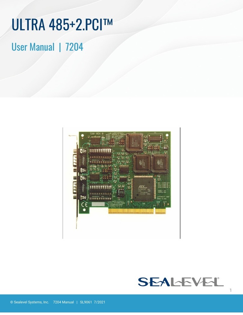
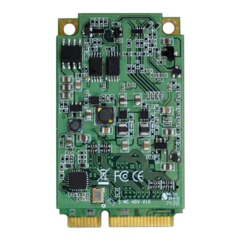
BitFlow NEO-PCE-CLB Quick user guide

The Neon
Hardware Reference Manual
BitFlow, Inc.
400 West Cummings Park, Suite 5050
Woburn, MA 01801
USA
Tel: 781-932-2900
Fax: 781-933-9965
Email: [email protected]
Web: www.bitflow.com
Revision G.5

© 2016 BitFlow, Inc. All Rights Reserved.
This document, in whole or in part, may not be copied, photocopied, reproduced, trans-
lated or reduced to any other electronic medium or machine readable form without the
prior written consent of BitFlow, Inc.
BitFlow, Inc. makes no implicit warranty for the use of its products and assumes no
responsibility for any errors that may appear in this document, nor does it make a commit-
ment to update the information contained herein.
BitFlow, Inc. retains the right to make changes to these specifications at any time without
notice.
All trademarks are properties of their respective holders.
Revision History:
Revision Date Comments
F.0 2007-02-01 First Revision
G.0 2008-04-25 Synchronized with SDK 5.00
G.1 2009-07-01 Synchronized with SDK 5.20
G.2 2009-09-10 Added NEO-PCE-CLD and NEO-PCE-CLB Revi-
sion 2
G.3 2010-11-18 Added NEO-PCE-CLQ
G.4 2016-04-18 Added NEO-PCE-DIF
G.5 2016-04-28 Minor corrections

Table of Contents
BitFlow, Inc.
Table of Contents
P - Preface
Purpose NEO-P-1
Support Services NEO-P-1
Technical Support NEO-P-1
Sales Support NEO-P-1
Conventions NEO-P-2
1 - General Description and Architecture
The Neon NEO-1-1
NEO-PCE-CLB General Description NEO-1-2
NEO-PCE-CLD General Description NEO-1-4
NEO-PCE-CLQ General Description NEO-1-6
NEO-PCE-DIF General Description NEO-1-8
Virtual vs Hardware Frame Grabbers NEO-1-10
The Virtual Frame Grabber (VFG) NEO-1-10
Configuration Spaces NEO-1-10
Firmware, Camera Files and Downloads NEO-1-11
2 - Acquisition and Camera Control
Introduction NEO-2-1
BitFlow’s Flow-Thru Architecture NEO-2-2
Camera Specific Firmware for Camera Link Models (CL Models Only) NEO-2-7
Generation of Acquisition Windows NEO-2-9
The Horizontal Active Window, HAW NEO-2-9
The Vertical Active Window, VAW NEO-2-10
The Control Tables (CTABs) NEO-2-12
Vertical Control Table NEO-2-12
The VCTAB Functions NEO-2-13
Vertical Control Table Size NEO-2-15
Horizontal Control Table NEO-2-15
The HCTAB Functions NEO-2-17
Horizontal Control Table Size NEO-2-20
Synchronizing Acquisition, Camera, CTABs and External Signals NEO-2-21
Vertical Operations and Events NEO-2-21
Horizontal Operations and Events NEO-2-25
Acquisition Command and Status NEO-2-29
The Acquisition Bitfields NEO-2-29
Trigger Processing (CL & Dif Models Only) NEO-2-34
Encoder Processing (CL & Dif Models Only) NEO-2-35
The On-Board Signal Generator NEO-2-36

Table of Contents
BitFlow, Inc.
3 - New Timing Generator
Introduction NEO-3-1
Components and Control NEO-3-2
Periods and Frequencies NEO-3-2
Waveform polarity NEO-3-3
Triggering NEO-3-3
Output Signals NEO-3-3
Master/Slave Control NEO-3-3
Timing NEO-3-4
NTG Control Registers NEO-3-5
4 - Quadrature Encoder
Introduction NEO-4-1
Simple Encoder Mode NEO-4-1
Positive or Negative Only Acquisition NEO-4-1
Interval Mode NEO-4-2
Re-Acquisition Prevention NEO-4-2
Scan Step Mode NEO-4-2
Combining Modes NEO-4-2
Control Registers NEO-4-2
Observability NEO-4-3
Electrical Connections NEO-4-3
Understanding Stage Movement vs. Quadrature Encoder Modes NEO-4-4
CON15 Register NEO-4-6
CON16 Register NEO-4-10
CON22 Register NEO-4-12
CON51 Register NEO-4-14
5 - Encoder Divider
Introduction NEO-5-1
Encoder Divider Details NEO-5-2
Formula NEO-5-2
Example NEO-5-2
Restrictions NEO-5-2
PLL Locking NEO-5-3
Handling Encoder Slow Down or Stopping NEO-5-3
Encoder Divider Control Registers NEO-5-4
6 - Power Over Camera Link (PoCL)
Introduction NEO-6-1
PoCL Compatibility NEO-6-2
PoCL Safe Power NEO-6-3
PoCL Control Registers NEO-6-5

Table of Contents
BitFlow, Inc.
7 - System Status
Introduction NEO-7-1
FACTIVE, FCOUNT NEO-7-2
PCOUNT, LCOUNT, FENCOUNT NEO-7-3
RD_TRIG_DIFF/TTL/OPTO, RD_ENC_DIFF/TTL/OPTO NEO-7-4
TRIG_QUALIFIED NEO-7-5
VCOUNT, HCOUNT, LINES_TOGO NEO-7-6
FIFO_EQ NEO-7-7
DEST_ADD NEO-7-8
8 - Camera Control Registers
Introduction NEO-8-1
Bitfield definitions NEO-8-2
Example Bitfield Definition NEO-8-2
Bitfield Definition Explanation. NEO-8-2
CON0 Register NEO-8-4
CON1 Register NEO-8-8
CON2 Register NEO-8-15
CON3 Register NEO-8-21
CON4 Register NEO-8-24
CON5 Register NEO-8-31
CON6 Register NEO-8-37
CON7 Register NEO-8-39
CON8 Register NEO-8-42
CON9 Register NEO-8-48
CON10 Register NEO-8-52
CON11 Register NEO-8-56
CON12 Register NEO-8-58
CON13 Register NEO-8-60
CON14 Register NEO-8-62
CON15 Register NEO-8-66
CON16 Register NEO-8-70
CON17 Register NEO-8-73
CON18 Register NEO-8-75
CON19 Register NEO-8-77
CON20 Register NEO-8-79
CON21 Register (Bayer Version) NEO-8-82
CON22 Register NEO-8-85
CON23 Register NEO-8-87
CON24 Register NEO-8-89
CON25 Register NEO-8-93
CON26 Register NEO-8-95
CON27 Karbon Register NEO-8-97
CON27 Neon-DIF Register NEO-8-99
CON36 Register NEO-8-101
CON37 Register NEO-8-103
CON38 Register NEO-8-105

Table of Contents
BitFlow, Inc.
CON40 Register NEO-8-108
CON41 Register NEO-8-110
CON42 Register NEO-8-112
CON43 Register NEO-8-118
CON44 Register NEO-8-120
CON51 Register NEO-8-122
9 - Karbon/Neon/Alta DMA
Introduction NEO-9-1
CON28 Register NEO-9-2
CON29 Register NEO-9-4
CON30 Register NEO-9-6
CON31 Register NEO-9-8
CON32 Register NEO-9-10
CON33 Register NEO-9-12
CON34 Register NEO-9-14
CON35 Register NEO-9-17
Scatter Gather DMA Instructions NEO-9-19
Destination Address NEO-9-20
Size of Transfer NEO-9-21
Next Quad Address NEO-9-22
10 - Register and Memory Mapping
Introduction NEO-10-1
Memory Types NEO-10-2
Registers NEO-10-2
UART NEO-10-2
DPM NEO-10-2
CTABs NEO-10-2
Memory Map NEO-10-3
Downloading Firmware NEO-10-5
PCI Configuration Space and Model/Revision Information NEO-10-6
11 - Electrical Interfacing
Introduction NEO-11-1
Trigger NEO-11-2
Trigger Input Types NEO-11-2
The Optocoupled Trigger NEO-11-2
Encoder NEO-11-4
Encoder Input Types NEO-11-4
The Optocoupled Encoder NEO-11-4
General Purpose Inputs (GPIN) NEO-11-6
Introduction NEO-11-6
General Purpose Outputs (GPOUT) NEO-11-7

Table of Contents
BitFlow, Inc.
Introduction NEO-11-7
GPOUT Open Collector Drivers NEO-11-7
Camera Link Controls (CCs) NEO-11-10
12 - Specifications
Introduction NEO-12-1
Maximum Pixels Per Line NEO-12-3
Maximum Lines Per Frame NEO-12-4
Power Consumption NEO-12-5
13 - Mechanical
Introduction NEO-13-1
The NEO-PCE-CLB Revision 1 NEO-13-2
The NEO-PCE-CLB Revision 2 NEO-13-3
The NEO-PCE-CLD NEO-13-4
The NEO-PCE-CLQ NEO-13-5
The NEO-PCE-DIF NEO-13-7
The Neon Connectors NEO-13-8
The CL Connectors NEO-13-8
The I/O Connectors NEO-13-8
The Jumpers NEO-13-10
Switches NEO-13-11
Switch S1, All Neon models NEO-13-11
Switch S2, NEO-PCE-CLB Revision 2 Only NEO-13-11
Switches S3 and S6, NEO-PCE-CLB Revision 2 Only NEO-13-11
Switches S4 and S7, NEO-PCE-CLB Revision 2 Only NEO-13-12
Switch S5, NEO-PCE-CLB Revision 2 Only NEO-13-12
The Camera Link Connector Pinouts (CL1 to CL4) NEO-13-13
NEO-PCE-CLB Revision 1 I/O Connector, Standard Configuration (P10) NEO-13-14
NEO-PCE-CLB Revision 1 I/O Connector, Alternate Configuration (P10) NEO-13-15
NEO-PCE-CLB Revision 2 I/O Connector (P10) NEO-13-16
NEO-PCE-CLD I/O Connector Pinout (P1) NEO-13-17
NEO-PCE-CLQ I/O Connector Pinout (P3) NEO-13-19
NEO-PCE-DIF Main Connector Pinout (P7) NEO-13-22
NEO-PCE-DIF Auxiliary Connector Pinout (P2) NEO-13-25
NEO-PCE-DIF I/O Connector Pinout (P3) NEO-13-27

-TOC-6 BitFlow, Inc. Version

Preface Purpose
Version G.5 BitFlow, Inc. NEO-P-1
Preface
Chapter P
P. 1 Pu r p o s e
This Hardware Reference Manual is intended for anyone using the Neon family of
frame grabber. The purpose of this manual is two-fold. First, this manual completely
describes how the board works. Second, it is a reference manual describing in detail
the functionality of all of the board’s registers.
P.1.1 Support Services
BitFlow, Inc. provides both sales and technical support for the Neon family of prod-
ucts.
P.1.2 Technical Support
Our web site is www.bitflow.com.
Technical support is available at 781-932-2900 from 9:00 AM to 6:00 PM Eastern Stan-
dard Time, Monday through Friday.
For technical support by email (support@bitflow.com) or by FAX (781-933-9965),
please include the following:
Product name
Camera type and mode being used
Software revision number
Computer CPU type, PCI chipset, bus speed
Operating system
Example code (if applicable)
P.1.3 Sales Support
Contact your local BitFlow Sales Representative, Dealer, or Distributor for information
about how BitFlow can help you solve your most demanding camera interfacing
problems. Refer to the BitFlow, Inc. web site (www.bitflow.com) for a list of North
American representatives and worldwide distributors.

Purpose The Neon
NEO-P-2 BitFlow, Inc. Version G.5
P.1.4 Conventions
Table P-1 shows the conventions that are used for numerical notation in this manual.
Table P-2 shows the numerical abbreviations that are used in this manual.
Table P-1 Base Abbreviations
Base Designator Example
Binary b 1010b
Decimal None 4223
Hexidecimal h 12fah
Table P-2 Numeric Abbreviations
Abbreviation Value Example
K 1024 256K
M 1048576 1M

General Description and Architecture The Neon
Version G.5 BitFlow, Inc. NEO-1-1
General Description and Architecture
Chapter 1
1.1 The Neon
The purpose of this chapter is to explain, at a block diagram level, how the Neon fam-
ily works, and what different versions are available. There are a few models in the
Neon family:
NEO-PCE-CLB, supports one base CL cameras (Revision 1 and Revision 2)
NEO-PCE-CLD, supports two base CL cameras
NEO-PCE-CLQ, supports four base CL cameras
NEO-PCE-DIF, supports one differential camera

NEO-PCE-CLB General Description The Neon
NEO-1-2 BitFlow, Inc. Version G.5
1.2 NEO-PCE-CLB General Description
Figure 1-1 illustrates the block diagram of the NEO-PCE-CLB.
Figure 1-1 NEO-PCE-CLB Block Diagram
The NEO-PCE-CLB implements the Camera Link base configuration, i.e. it can accept
a single camera putting out up to 24 bits of data.
The NEO-PCE-CLB can accept input data at up to 85 Mhz.
The following paragraphs are a short description of each block.
The Camera Link Interface block implements the CL base configuration This block has
the Channel Link IC, the Camera Control drivers and the serial communication trans-
ceivers.
The MUX block packs and assembles the data from the Camera Link block before it is
pushed into the FIFO. This block re-arranges on-the-fly the data from the camera’s
taps so that the data is written in raster scan format in the host memory.
24 64
64
64 64
64
64
64
Camera Link
Interface
MUX
Video Pipeline,
Data Packer
PCI Interface,
Scatter-Gather
DMA Engine
Camera
Control,
CTABs
FIFO
I/O,
Triggers,
Encoders
UART
Serial
Interface
P10
Local Bus
PCI Express Bus
CL1

General Description and Architecture NEO-PCE-CLB General Description
Version G.5 BitFlow, Inc. NEO-1-3
The FIFO block decouples the camera from the DMA engine. It is implemented with
dual ported memories.
The Camera Control block handles both camera synchronization as well as external I/
O. The block contains the CTABs which are uses to synchronize acquisition with the
camera, determine which pixels/lines get acquired and which do not, generate con-
trol signals to the camera and to external devices. This block also handles start/stop-
ping acquisition based on triggers and encoders.
The PCI interface block handles host reads/writes to/from the board. These reads/
writes are used to program the board, and to control its modes. This block is also
responsible for DMAing image data to the host memory (or other devices). The DMA
engine uses chaining scatter-gather DMA, which can DMA a virtually unlimited
amount of data to memory without using any CPU cycles.
There is an on-board UART, as required by the CL specification.
The IO connector block has transmitters/receivers to communicate with external
industrial equipment (triggers, encoders, light strobes etc.).

NEO-PCE-CLD General Description The Neon
NEO-1-4 BitFlow, Inc. Version G.5
1.3 NEO-PCE-CLD General Description
Figure 1-2 illustrates the block diagram of the NEO-PCE-CLD.
Figure 1-2 NEO-PCE-CLD Block Diagram
The NEO-PCE-CLD implements two completelys separate Camera Link base inter-
faces. Each interface is really a completely independent Virtual Frame Grabber (VFG).
Put another way, the NEO-PCE-CLD has two complete copies of the NEO-PCE-CLB as
shown in Figure 1-1. The main difference being that both VFGs share a common I/O
connector (P1).
Each VFG can accept up to 24 bits at up to 85 Mhz pixel clock frequency.
The following paragraphs are a short description of each block.
CL
Connector
2
UART
PCI
Device
1
PCI
Device
0
Channel
Link
Chip
UART
Channel
Link
Chip
Acquisition
and
Control
Logic
Acquisition
and
Control
Logic
PCI Express Bus
CL2
CL
Connector
1
CL1
P1

General Description and Architecture NEO-PCE-CLD General Description
Version G.5 BitFlow, Inc. NEO-1-5
The Camera Link Interface block implements the CL base configuration This block has
the Channel Link chip, the Camera Control drivers and the serial communication tran-
ceivers. Note that each VFG has its own UART so that serial communications to both
cameras can happen simultaneously.
The MUX block packs and assembles the data from the Camera Link block before it is
pushed into the FIFO. This block re-arranges on-the-fly the data from the camera’s
taps so that the data is written in raster scan format in the host memory.
The FIFO block decouples the camera from the DMA engine. It is implemented with
dual ported memories.
The Camera Control block handles both camera synchronization as well as external I/
O. The block contains the CTABs which are uses to synchronize acquisition with the
camera, determine which pixels/lines get acquired and which do not, generate con-
trol signals to the camera and to external devices. This block also handles start/stop-
ping acquisition based on triggers and encoders.
The PCI interface block handles host reads/writes to/from the board. These reads/
writes are used to program the board, and to control its modes. This block is also
responsible for DMAing image data to the host memory (or other devices). The DMA
engine uses chaining scatter-gather DMA, which can DMA a virtually unlimited
amount of data to memory without using any CPU cycles.
There is an on-board UART, as required by the CL specification.
The IO connector block has transmitters/receivers to communicate with external
industrial equipment (triggers, encoders, light strobes etc.).

NEO-PCE-CLQ General Description The Neon
NEO-1-6 BitFlow, Inc. Version G.5
1.4 NEO-PCE-CLQ General Description
Figure 1-3 illustrates the block diagram of the NEO-PCE-CLQ.
Figure 1-3 NEO-PCE-CLQ Block Diagram
The NEO-PCE-CLQ implements four completelys separate Camera Link base inter-
faces. Each interface is really a completely independent Virtual Frame Grabber (VFG).
Put another way, the NEO-PCE-CLQ has four complete copies of the NEO-PCE-CLB as
shown in Figure 1-1. The main difference being that all VFGs share a common I/O
connector (P1).
Each VFG can accept up to 24 bits at up to 85 Mhz pixel clock frequency.
PCI
Device
0
Acquisition
and
Control
Logic
CL
Connector
1
UART
Channel
Link
Chip
CL1
PCI
Device
1
Acquisition
and
Control
Logic
CL
Connector
2
UART
Channel
Link
Chip
CL2
PCI
Device
2
Acquisition
and
Control
Logic
CL
Connector
3
UART
Channel
Link
Chip
CL3
PCI
Device
3
Acquisition
and
Control
Logic
CL
Connector
4
UART
Channel
Link
Chip
CL4
P1
PCI Express Bus

General Description and Architecture NEO-PCE-CLQ General Description
Version G.5 BitFlow, Inc. NEO-1-7
The following paragraphs are a short description of each block.
The Camera Link Interface block implements the CL base configuration This block has
the Channel Link chip, the Camera Control drivers and the serial communication tran-
ceivers. Note that each VFG has its own UART so that serial communications to both
cameras can happen simultaneously.
The MUX block packs and assembles the data from the Camera Link block before it is
pushed into the FIFO. This block re-arranges on-the-fly the data from the camera’s
taps so that the data is written in raster scan format in the host memory.
The FIFO block decouples the camera from the DMA engine. It is implemented with
dual ported memories.
The Camera Control block handles both camera synchronization as well as external I/
O. The block contains the CTABs which are uses to synchronize acquisition with the
camera, determine which pixels/lines get acquired and which do not, generate con-
trol signals to the camera and to external devices. This block also handles start/stop-
ping acquisition based on triggers and encoders.
The PCI interface block handles host reads/writes to/from the board. These reads/
writes are used to program the board, and to control its modes. This block is also
responsible for DMAing image data to the host memory (or other devices). The DMA
engine uses chaining scatter-gather DMA, which can DMA a virtually unlimited
amount of data to memory without using any CPU cycles.
There is an on-board UART, as required by the CL specification.
The IO connector block has transmitters/receivers to communicate with external
industrial equipment (triggers, encoders, light strobes etc.).

NEO-PCE-DIF General Description The Neon
NEO-1-8 BitFlow, Inc. Version G.5
1.5 NEO-PCE-DIF General Description
Figure 1-4 illustrates the block diagram of the NEO-PCE-DIF
Figure 1-4 NEO-PCE-DIF Block Diagram
The NEO-PCE-DIF supports one differential camera up to 32 bits.
The NEO-PCE-DIF can accept input data at up to 85 Mhz.
The following paragraphs are a short description of each block.
The MUX block packs and assembles the data from the Camera Link block before it is
pushed into the FIFO. This block re-arranges on-the-fly the data from the camera’s
taps so that the data is written in raster scan format in the host memory.
The FIFO block decouples the camera from the DMA engine. It is implemented with
dual ported memories.
16
16
64
64
64 64
64
64
64
MUX
Video Pipeline,
Data Packer
PCI Interface,
Scatter-Gather
DMA Engine
Camera
Control,
CTABs
FIFO
UART
Serial
Interface
Local Bus
PCI Express Bus
P2
Bits 16 to 31
P7
Bits 0 to 15

General Description and Architecture NEO-PCE-DIF General Description
Version G.5 BitFlow, Inc. NEO-1-9
The Camera Control block handles both camera synchronization as well as external I/
O. The block contains the CTABs which are uses to synchronize acquisition with the
camera, determine which pixels/lines get acquired and which do not, generate con-
trol signals to the camera and to external devices. This block also handles start/stop-
ping acquisition based on triggers and encoders.
The PCI interface block handles host reads/writes to/from the board. These reads/
writes are used to program the board, and to control its modes. This block is also
responsible for DMAing image data to the host memory (or other devices). The DMA
engine uses chaining scatter-gather DMA, which can DMA a virtually unlimited
amount of data to memory without using any CPU cycles.
There is an on-board UART which can be use with cameras that support serial commu-
nications.
The IO connector block has transmitters/receivers to communicate with external
industrial equipment (triggers, encoders, light strobes etc.).

Virtual vs Hardware Frame Grabbers The Neon
NEO-1-10 BitFlow, Inc. Version G.5
1.6 Virtual vs Hardware Frame Grabbers
It’s important to understand how this manual works. Some chapters of this manual dis-
cuss the NEO-PCE-CLD and NEO-PCE-CLQ as a hardware platforms (this chapter is a
good example). While other chapters discuss the details of the Virtual Frame Grab-
bers (VFG) that this hardware platform supports. The concept of the virtual frame
grabber is described below, but basically the idea is that one hardware platform can
support more than one device. In the case of the Karbon-CL, these devices are frame
grabbers.
Note that we are not using the word virtual here in the sense of “a software virtualiza-
tion of a hardware device”, these VFGs are real hardware. The reason we using “vir-
tual” is because the term “frame grabber” has more than one meaning. It can mean
the piece of hardware that you put in your computer, or it can mean the device that
the your software application is controlling and getting images from. For the pur-
poses of this manual, “virtual frame grabber” means the device that your application
is interfacing to. While this might sound complicated, the implementation is simple.
Plug a NEO-PCE-CLD or NEO-PCE-CLQ frame grabber into your PC, and your appli-
cation interacts with one or more VFGs available. Everything else is taken care of by
the BitFlow drivers.
1.6.1 The Virtual Frame Grabber (VFG)
The Karbon family was the first board from BitFlow that supports the concept of the
virtual frame grabber (VFG). The NEO-PCE-CLD and NEO-PCE-CLQ also use this con-
cept. The idea behind the VFG is to separate the hardware platform (connectors, lam-
inate, FPGAs, etc.) from the frame grabbing functionality that software applications
work with. The primary reason behind this separation is that the turn around time for
hardware is much longer than the turn around time for modifying virtual frame grab-
bers. To create a brand new virtual frame grabber, or to modify an existing one, sim-
ply requires writing new firmware or updating existing firmware.
The idea of modifying a frame grabber by making changes to its firmware is not new.
BitFlow has been doing this since its very first product. However, what is new about
the Karbon family, is the fact the entire frame grabber is written in firmware. The only
fixed hardware components are the interfaces to the outside world (e.g. the CL chips
on the front end). Everything else that makes up the board, camera control, data buff-
ering, DMA engine, etc. is written in firmware. This gives the Karbon platform incredi-
ble levels of flexibility and opens the door to unlimited customization.
1.6.2 Configuration Spaces
The NEO-PCE-CLD supports two VFGs, the NEO-PCE-CLQ supports four VFGs. Each
VFG has its own configuration space (PCI interface) and will look like a separate
device to the operating system. Each VFG has its own CL interface chip. Figure 1-2
shows the block diagram of the entire board, while Figure 1-1 shows the block dia-
gram of the individual VFG. In this case, each VFG looks like a separate instance of the
single base Neon.
This manual suits for next models
3
Table of contents
Other BitFlow PCI Card manuals
