BWI ENDAT-3201M User manual

ENDAT-3201M/MF/MH
User’s Manual
Rev. 2x
For 3201M PCB ver.1F or later
For 3201MF/MH PCB ver.1B or later
1/16/2003
II
The low power consumption CPU embedded board
Copyright Notice
The content of this manual has been checked for accuracy. The manufacturer assumes no
responsibility for any inaccuracies that may be contained in this manual. The manufacturer
reserves the right to make improvements or modification to this document and/or the
product at any time without prior notice. No part of this document may be reproduced,
transmitted, photocopied or translated into any language, in any form or by any means,
electronic, mechanical, magnetic, optical or chemical, without the prior written permission
of the manufacturer.
VIA is registered trademark of VIA Technology Incorporation
VT82C686B may only be used to identify products of VIA Technology
Realtek is registered trademark of Realtek Technologies Inc.
Multiscan is a trademark of Sony Corp of America
IBM, EGA, VGA, PC/XT, PC/AT, OS/2 and PS/2 are registered trademarks of International
Business Machines Corporation
Intel is a registered trademark of Intel Corporation
Plug and Play is registered trademarks of Intel Corporation
Microsoft, Windows and MS-DOS are trademarks of Microsoft Corporation
AMI is a trademark of American Megatrends Inc.
PCI is a registered trademark of PCI Special Interest Group
Other product names mentioned herein are used for identification purpose only and may be
trademarks and/or registered trademarks of their respective companies.
Installation Notice
The manufacturer recommends using a grounded plug to ensure proper motherboard
operation. Care should be used in proper conjunction with a grounded power receptacle to
avoid possible electrical shock. All integrated circuits on this motherboard are sensitive to
static electricity. To avoid damaging components from electrostatic discharge, please do not
remove the board from the anti-static packing before discharging any static electricity to
your body, by wearing a wrist-grounding strap. The manufacturer is not responsible for any
damage to the motherboard due to improper operation.

User’s Manual
III
Specification:
This manual covers three different layout models, and the respective board layouts
are shown in chapter 1-4. Please refer to the following description to make sure
which model on hand before using.
ENDAT-3201M ENDAT-3201MF ENDAT-3201MH
System Chipset VIA VT8601A + VIA VT82C686B (APOLLO PLE-133)
Micro Processor Embedded Low Power Consumption VIA Eden 533 MHz or C3-800 MHz CPU
Memory 1 DIMM Socket up to 512MB (max)
Ethernet 10/100 BaseT LAN onboard (Realtek 8139C or Intel 82559ER)
LCD / VGA Support 24 Bits TFT LCD Panel with 2D / 3D Graphic Controller, SMA up to 8MB
IDE Connector 1x Enhance IDE Connectors Support UDMA 33/66/100
FDD Connector 1x FDD Connector
Expansion Slot 1x 188Pin EISA Connector for PCI/ISA expansion.
Flash Memory Reserved Socket for DOC 2000 support
Keyboard / Mouse Double-Deck + Pin Header Double-Deck + Pin Header Pin Header
LAN/USB USB+LAN Double-Deck USB+LAN Double-Deck
& USB Pin Header
USB Pin Header
RJ-45 LAN Jack
COM 1 Double-Deck
(COM 1+LPT1+VGA)
Double-Deck
(COM 1+LPT1+VGA) Box Header
COM 2 D-SUB D-SUB Box Header
COM 3 D-SUB Box Header Box Header
COM 4 D-SUB Box Header Box Header
LPT 1 Double-Deck
(COM1+LPT 1+VGA)
Double-Deck
(COM1+LPT 1+VGA) Box Header
LPT 2 Box Header Box Header Box Header
VGA Double-Deck
(COM1+LPT1+VGA)
Double-Deck
(COM1+LPT1+VGA)
& Box Header for VGA
Box Header
TFT LCD Connector 44 Pin Box Header
LVDS output Optional LVDS for LCD output via 16 Pin Header.
Watch Dog Timer Optional programmable Watch Dog Timer support 1-255s.
RS-422/485 Optional via COM2
COM Port Power 4 Serial port support Standard RI. / +5V / +12V power via Pin 9
Boot ROM Reserve Socket for Boot ROM
Power Supply AT or ATX Power support.
Form Factor SBC / 203mm x 146mm (7.99” x 5.74”)
IV
The low power consumption CPU embedded board

TABLE OF CONTENTS
CHAPTER 1. INTRODUCTION............................................................. 1
1-1. FEATURES............................................................................................................2
1-2. UNPACKING ........................................................................................................5
1-3. ELECTROSTATIC DISCHARGE PRECAUTIONS ............................................5
1-4. MOTHERBOARD LAYOUT (ENDAT-3201M)..................................................6
1-5. MOTHERBOARD LAYOUT (ENDAT-3201MF) ..............................................7
1-6. MOTHERBOARD LAYOUT (ENDAT-3201MH) ..............................................8
CHAPTER 2. SETTING UP THE MOTHERBOARD..........................9
2-1. JUMPERS AND CONNECTORS (ENDAT-3201M) ............................................9
2-2. JUMPERS AND CONNECTORS (ENDAT-3201MF)........................................15
2-3. JUMPERS AND CONNECTORS (ENDAT-3201MH) .......................................23
2-4. INSTALLING MEMORY ....................................................................................30
2-5. SHARED VGA MEMORY ..................................................................................30
2-6. INSTALLING RISER CARD...............................................................................30
2-7. ASSIGNING IRQs FOR EXPANSION CARDS..................................................31
2-8. ASSIGNING DMA CHANNELS FOR ISA CARDS...........................................32
CHAPTER 3. AMI BIOS SETUP ..........................................................33
3-1. QUICK SETUP.....................................................................................................34
3-2. DESCRIPTION OF BIOS SETUP OPTIONS......................................................34
3-3. ADVANCED CMOS SETUP ...............................................................................35
3-4. DETAILS OF THE ADVANCED SHIPSET SETUP ...........................................37
3-5. PERIPHERALS SETUP.......................................................................................39
3-6. POWER MANAGEMENT SETUP......................................................................42
3-7. PCI PLUG AND PLAY SETUP ...........................................................................44
3-8. HARDWARE MONITOR SETUP .......................................................................46
VI
The low power consumption CPU embedded board
CHPATER 4. VGA, LCD, DOC FEATURE .........................................47
4-1. AGP-BUS VGA FEATURE..................................................................................47
4-2. LCD FLAT PANEL FEATURE ............................................................................48
4-3. PCI BUS AUDIO ADAPTER FEATURE ............................................................49
4-4. DISKONCHIP FEATURE ....................................................................................50
4-5. DRIVER UTILITY INSTALLATION GUIDE ....................................................51
CHPATER 5. LAN ADAPTER...............................................................53
5-1. FEATURES...........................................................................................................53
5-2. UTP CABLE/RJ-45 JACK DEFINITION............................................................54
5-3. CONNECTING 100BASE-TX FAST ETHERNET NETWORK ........................55
5-4. CONNECTING 10BASE-T ETHERNET NETWORK .......................................55
5-5. 10M BASE/100MBASE INSTALLATION NOTICE ..........................................55
5-6. REMOTE BOOT ROM INSTALLATION GUIDE..............................................56
5-7. LED INDICATORS ..............................................................................................57
5-8. SETUP PROGRAM .............................................................................................57
5-9. LAN DRIVER INSTALLATION PROCEDURE.................................................60
APPENDIX A: FLASH MEMORY UTILITY ..................................... 61
APPENDIX B: CONNECTOR PIN ASSIGNMENT ........................... 63
APPENDIX C: LIMITED WARRANTY .............................................. 71

Chapter 1. Introduction
In order to cope with the challenges of the heating issues and demand of much more
diminutive embedded system in diverse application, ENDAT-3201M/MF/MH series CPU
boards provides the ultimate solution by integrating with VIA’s technology low power
consumption VIA C3 series CPU and VIA EDEN fanless ESP series CPU. ENDAT-3201M
series CPU boards offer the assorted functions for various applications such as high-end POS
systems, kiosks, networking systems, controlling terminals and other embedded systems.
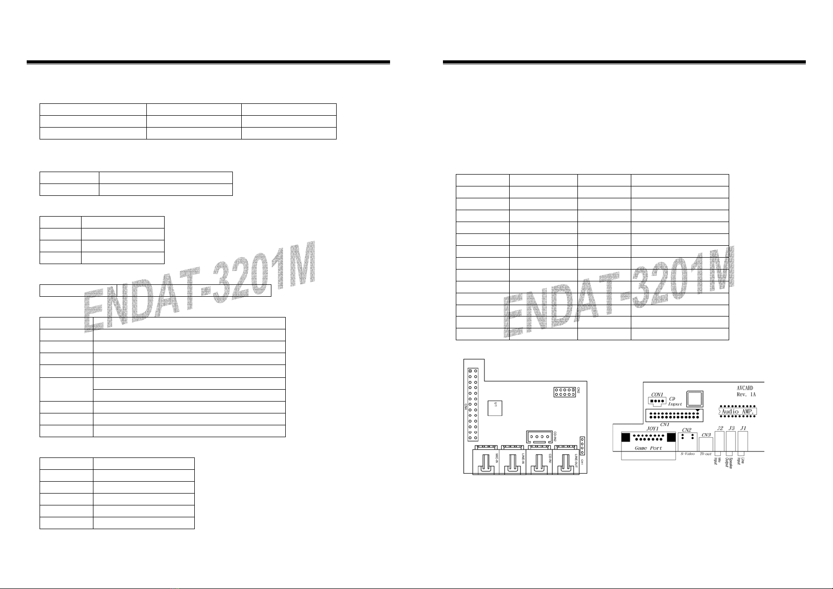
ENDAT-3201M/MF/MH is a 5.25” SBC uses
VIA chipsets built-in VGA and Audio
feature onboard, support TFT TTL LCD feature with LVDS interface as feature option;
i
ntegrated Super-I/O support 4 Serial with power selector and 2 parallel ports,
built-in Realtek 8139x LAN chipset with RJ45 Jack for 10BaseT/ 100BaseT. The option of
Intel 82559/ER chip is also provided for the LAN support. This SBC offers the highest
performance PC specification in the industry with embedded low power consumption VIA
EDEN Fanless ESP series CPU ESP5000, and with the option of the higher performed VIA
C3 800MHz CPU. For easier assembly and better integration without arranging array of
cables, the ENDAT-3201M/MF provides onboard connectors with a similar conventional
ATX IO connector layout; as for ENDAT-3201MH leaves the flexibilities of cable
connections similar to the standard 5.25” SBC.
ENDAT-3201M/MF/MH provides the option of integrating Watch Dog Timer for
ideal unattended terminals. To offer better flexibility, it also provides the options of
riser card for PCI or ISA expansion through a 188-pin slot. This CPU board is fully
compatible with industry standards, adding many technical enhancements and are
fully compatible with thousand of software application such as WIN 95, 98, WIN
NT 3.x / 4.x, WIN 2000, WIN ME, WIN CE (.NET), Linux, UNIX, Novell…etc.
The control logic provides high-speed performance for the most advanced
multi-user, multitasking application available today. “Tomorrow’s PC technology
is here today”.
2
The ENDAT-3201M/MF/MH
Embedded CPU Board
1-1. Features
Basic Feature:
zENDAT-3201M/MF/MH, embedded VIA
C3
TM
, Eden
TM
, Ezra
TM
Low
Power EBGA processors.
z133 / 100 MHz CPU Front Side Bus (FSB)
zDRAM interface synchronous or pseudo synchronous with CPU FSB speed
of 133 / 100 / 66 MHz Mixed 1M / 2M / 4M / 8M / 16M / 32MxN DRAMs
z1 DIMM 168 Pin socket supported up to 512MB
z3.3V DRAM interface with 5V-tolerant inputs
zSupport single channel support two UltraDMA-100 / 66 / 33 enhance IDE
zAC-97 link.
zOn-board built-in 2 USB ports.
zIntegrated Super-I/O support 4 Serial with power selector and 2 parallel
ports.
zOptional RS-422/485 via COM2
zSystem Hardware monitoring
zKeyboard / mouse interfaces.
zRTC / CMOS
zPCI-2.0 compliant, 32 bit with 5V tolerant inputs.
z33 MHz operation on the primary PCI bus
z188pin expansion slot for both PCI and ISA Bus signals.
zPC99 Hardware Support
zWatch-Dog-Timer support 1-255sec programmable.
zOn-board support Realtek or Intel 82559/ER 10/100 LAN adapter with
RJ-45 port.
zAGP v2.x compliant
zIntegrated AGP Bus 2D / 3D graphic accelerator.
zWindows 95 OSR-2 VXD and integrated Windows 98 / NT 4.0 miniport
driver support
zBIOS shadow at 16KB increment

User’s Manual
3
zSupports 2, 4 and 8 Mbytes of Frame Buffer with share memory.
zDirectDrawTM and DirectVideoTM Hardware Support
zAdvanced Mobile Power Management
zCRT Power Management (VESA™ DPMS)
Optional for Flat Panel Interface (TTL or LVDS)
The board is designed to support industry standard TFT panel via 44pin connector
or LVDS transmitters. The interface supports both 18-bit and 24-bit display modes.
Optionally, an 18+18 panel can be supported utilizing external latches.
Optional Features
•
Supports RS422/RS485 interface with COM2
•
Support LVDS LCD panel
•
Supports Audio function (via AV Card Kit)
•
Supports TV-Out feature (via TV-Out adapter Kit)
•
Support Watch Dog Timer
•
Support BOOT ROM
Ordering information:
ENDAT-3201M
1. ENDAT-3201M-1R: Support 1 Realtek LAN
2. ENDAT-3201M-1i: Support 1 Intel LAN
3. ENDAT-3201M-1RL: Support 1 Realtek LAN + LVDS
4. ENDA-3201M-1iL: Support 1 Intel LAN + LVDS
ENDAT-3201MF
1. ENDAT-3201MF-1R: Support 1 Realtek LAN
2. ENDAT-3201MF-1i: Support 1 Intel LAN
3. ENDAT-3201MF-1RL: Support 1 Realtek LAN + LVDS
4. ENDA-3201MF-1iL: Support 1 Intel LAN + LVDS
4
The ENDAT-3201M/MF/MH
Embedded CPU Board
ENDAT-3201MH
1. ENDAT-3201MH-1R: Support 1 Realtek LAN
2. ENDAT-3201MH-1i: Support 1 Intel LAN
3. ENDAT-3201MH-1RL: Support 1 Realtek LAN + LVDS
4. ENDA-3201MH-1iL: Support 1 Intel LAN + LVDS
Note: The standard version of ENDAT-3201M/MF/MH is embedded with VIA EDEN
Fanless ESP5000. Other option CPUs will be provided upon request.

User’s Manual
5
1-2. Unpacking
The motherboard comes securely packaged in a sturdy cardboard shipping carton. In
addition to the User's Manual, the motherboard package includes the following items:
•
ENDAT-3201M/MF/MH 5.25” SBC / CPU Board
•
HDD/FDD Cables
•
TV-Out adapter / cable
(Optional)
•
Audio Kit
(Optional)
•
LCD cable
(Optional)
•
IDE Driver includes: Drivers for Windows NT 3.x/4.x, Windows 95, 98, 2000,
Win Me, Linux, Novell Netware and AMI FLASH ROM utilities.
•
Driver utilities for on-board VGA drivers, LAN adapter and DOC 2000
If any of these items are missing or damage, please contact the dealer from whom you
purchase the motherboard. Save the shipping material and carton in the event that you want
to ship or store the board in the future.
Note:
Leave the motherboard in its original package until you are ready to install it!
1-3. Electrostatic Discharge Precautions
Make sure you properly ground yourself before handling the motherboard, or other system
components. Electrostatic discharge can easily damage the components. Note: You must
take special precaution when handling the motherboard in dry or air-conditioned
environments.
6
The ENDAT-3201M/MF/MH
Embedded CPU Board
1-4. ENDAT-3201M

User’s Manual
7
1-5. ENDAT-3201MF
8
The ENDAT-3201M/MF/MH
Embedded CPU Board
1-6. ENDAT-3201MH

Chapter 2.
Setting up the CPU Motherboard
2-1. Jumpers and Connectors (ENDAT-3201M)
Jumpers/Connectors Overview:
Function Jumpers/Connectors
Cooling Fan Connector JFAN1, JFAN2
Power Supply: Power Good JP12: Pin 9~11
ATX Power On/Off Switch JP12: Pin 12~13
Audio Port Connector CN1
2
nd
Printer Port CN4
LAN Adapter Disable/Enable JP3
COM1 Port CN6
COM2 Port CN8
COM3 Port CN2
COM4 Port CN3
COM Ports Power Selector (COM1, 2, 3, 4) JP4, JP9
RS232/RS422/RS485 Selector (COM2) JP10, JP11
DiskOnChip Memory Address JP15
LCD: TFT LCD Panel Connector LCD-CON1
LVDS LCD Output Port CN5
LVDS Voltage Selector JP5
Clear CMOS JP2
Factory Setting JP1, JP7, JP8, JP13, JP14, JT1,
JH1
PS/2 Keyboard Jack JKBMS
PS/2 Mouse Jack JKBMS
PS/2 Mouse/KB Pin Header CN7
IR J1
FDD Connector FDD1
IDE 1 IDE1
Header for Case Panel JP12
10
The ENDAT-3201M/MF/MH
Embedded CPU Board
Function Jumpers/Connectors
IDE 1 LED JP12: Pin 1, Pin 2
External Speaker JP12: Pin 3, Pin 6
Buzzer On/Off JP12: Pin 4, Pin 5
Hardware Reset Switch JP12: Pin 7, Pin 8
External Power Good JP12: Pin 9, Pin 10
Internal Power Good JP12: Pin 10, Pin 11
ATX Power Supply On/Off Switch JP12: Pin 12, Pin 13
Power LED JP12: Pin 14, Pin 15
WDT Function Enable/Disable JP12: Pin 19, Pin 20
JP2: CMOS Data Clear:
Pin 1-2 * Normal
Pin 2-3 Clear CMOS Data
JP15: DiskOnChip Memory Address Selector
JP15 Memory Address
1-2 7-8
0C800H-0C9FFH
1-2 9-10
0CC00H-0CDFFH
3-4 7-8
0D000H-0D1FFH
3-4 9-10
0D400H-0D5FFH
5-6 7-8
0D800H-0D9FFH(Default)
JP3: On-board LAN Disable/Enable
Pin 1-2 Enable On-Board LAN
Pin 2-3 Disable On-Board LAN
JP9 (COM1, 2) / JP4 (COM3, 4) Voltage Selector:
Voltage COM1(JP9) COM2(JP9) COM3(JP4) COM4(JP4)
+12V(dc) 1-2 7-8 1-2 7-8
R.I. 3-4 9-10 3-4 9-10
+5V(dc) 5-6 11-12 5-6 11-12

User’s Manual
11
JP10, JP11: RS232 / 422 / 485 Selector for COM2
TYPE JP10 JP11
RS-232 1-2, 4-5, 7-8, 10-11 1-2
RS-422/485 Full Duplex 2-3, 5-6, 8-9, 11-12 3-4, 7-8
* Make sure the port mode is set up correctly before installing any peripherals.
JP12’s Pin 9~11: On-board Power Good Selector
Pin 9-10 Using External Power Good
Pin 10-11 Using On Board Power Good
JFAN1, JFAN2: CPU / 2nd Cooling Fan Connector
Pin No. Function
Pin 1 Sensor Pin.
Pin 2 +12V
Pin 3 GND
JP12’s Pin12;13: For ATX Power Supply
Pin 12; Pin 13 On/Off Switch for ATX Power
JP12: Case Panel Connection:
Pin No. Description
1,2 HDD_LED –/+
3,6 External Speaker
4,5 Onboard Buzzer
7-8 Hardware RESET
Reserved9-10
10-11 Reserved
12-13 ATX Power On/Off
14-15 Power LED (14:LED+, 15:LED–)
19-20 Close: Enable WDT function
J1: IR Pin Header.
Pin No. Function
1 +5V(DC)
2 N.C.
3 IRRX
4 GND.
5 IRTX
12
The ENDAT-3201M/MF/MH
Embedded CPU Board
CN1: Audio Output Port connector via AV Card Kit (Optional)
Please close pin13-14 to disable onboard Audio features if the AV Card Kit is not
inserted onto the CN1 connector. If AV card kit is inserted, please make sure the
BIOS is enabled with the audio function, since LPT2 and audio function can not be
used in the same time.
CN1: Audio Port.
Pin No. Function Pin No. Function
1 BITCLK 2 GND
3 SDIN 4 N.C.
5 SDIN2 6 N.C.
7 SDOUT 8 N.C.
9 SYNC 10 GND
11 –ACRST 12 GND
13 SPEAK 14 Strapping Low
15 +5V(DC) 16 +12V(DC)
17 JBCY 18 JAB2
19 JBCX 20 JAB1
21 JACY 22 JBB2
23 JACX 24 JBB1
25 MSO 26 MSI
AV Card
UC-A003

User’s Manual
13
CN7: Pin Header for PS2 KB / MS
Pin No. Signal (KB) Pin No. Signal(MS)
1 KB Data 2 MS Data
3 KEY 4 KEY
5 GND 6 GND
7 +5V(DC) 8 +5V(DC)
9 KB_CLK 10 MS_CLK
Printer (LPT1/LPT2) Port
Pin No. Description Pin No. Description
1 STB# 10 ACK#
2 PD0 11 BUSY
3 PD1 12 PE
4 PD2 13 SLCT
5 PD3 14 AFD#
6 PD4 15 ERR#
7 PD5 16 INIT#
8 PD6 17 SLIN#
9 PD7 18-25 GND
JP5: Voltage Selector for LDVS Receiver
Pin No. Signal
1-2 Receiver = +5V(DC) Type
2-3 Receiver = +3.3V(DC) Type
Open for OEM. Type4-5
Close for Normal Type
* Caution: Improper setting will damage LCD panel.
CN5: LCD - LVDS Output.
Pin No. Signal Pin No. Signal
1 Y0– 2 Y2–
3 Y0+ 4 Y2+
5 Y1– 6 Rcv. Voltage
7 GND 8 Y3–
9 Y1+ 10 Y3
11 CK– 12 VDD_PNL
13 CK+ 14 DISP_OFF
15 VBL 16 GND
14
The ENDAT-3201M/MF/MH
Embedded CPU Board
LCD_CON1: TFT LCD Panel Port
Pin No. Signal Pin No. Signal
1 VBL 2 VBL
3 GND 4 GND
5 VDDLCD 6 VDDLCD
7 ENPVEE 8 GND
9 FPD 23 10 FPD 22
11 FPD 17 12 FPD 16
13 FPD 11 14 FPD 10
15 FPD 9 16 FPD 8
17 FPD 21 18 FPD 20
19 FPD 15 20 FPD 14
21 FPD 7 22 FPD 6
23 FPD 5 24 FPD 4
25 FPD 19 26 FPD 18
27 FPD 13 28 FPD 12
29 FPD 3 30 FPD 2
31 FPD 1 32 FPD 0
33 GND 34 GND
35 P_CLK 36 FLM
37 DE 38 LP
39 GND 40 VDDLCD
41 VDDLCD 42 KEY
43 VDDLCD 44 VDDLCD
* Please make sure the Pin 1 location before inserting the LCD connector.
Please double-check the insertion and orientation of the LCD cable before applying power.
Improper installation will result in permanent damage LCD panel.
Factory Setting:
JP1: All Pin Open
JP7: LCD Voltage selector
Voltage JP7
3.3V 4-6
5V 2-4
JP8: Close Pin 1-2
JP13: Factory Using only
JP14: Close Pin 2-3; Pin 5-6; Pin 8-9; Pin 11-12
JT1: Close Pin 2-3; Pin 4-5; Pin 8-9
JH1: Close Pin 1-2; Pin 5-6; Pin 7-8

User’s Manual
15
2-2. Jumpers and Connectors (ENDAT-3201MF)
Jumpers/Connectors Overview:
Function Jumpers/Connectors
Cooling Fan Connector JFAN1, JFAN2
Power Supply: Power Good JP12: Pin 9~11
ATX Power On/Off Switch JP12: Pin 12~13
Audio Port Connector CN1
2
nd
Printer Port CN4
LAN Adapter Disable/Enable JP3
VGA Port VGA1 (D-SUB);
VGAC1 (16 Pin Box Header)
COM1 Port CN6
COM2 Port CN8
COM3 Port CN2
COM4 Port CN3
COM Ports Power Selector (COM1, 2, 3, 4) JP4, JP9
RS232/RS422/RS485 Selector (COM2) JP10, JP11
USB Port Double-Deck;
JUSB1 (Pin Header)
DiskOnChip Memory Address JP15
LCD: TFT LCD Panel Connector LCD-CON1
LVDS LCD Output Port CN5
LVDS Voltage Selector JP5
Clear CMOS JP2
Factory Setting JP1, JP7, JP8, JP13, JP14, JT1,
JH1
PS/2 Keyboard Jack JKBMS
PS/2 Mouse Jack JKBMS
PS/2 Mouse/KB Pin Header CN7
IR J1
FDD Connector FDD1
IDE 1 IDE1
16
The ENDAT-3201M/MF/MH
Embedded CPU Board
Function Jumpers/Connectors
Header for Case Panel JP12
IDE 1 LED JP12: Pin 1, Pin 2
External Speaker JP12: Pin 3, Pin 6
Buzzer On/Off JP12: Pin 4, Pin 5
Hardware Reset Switch JP12: Pin 7, Pin 8
External Power Good JP12: Pin 9, Pin 10
Internal Power Good JP12: Pin 10, Pin 11
ATX Power Supply On/Off Switch JP12: Pin 12, Pin 13
Power LED JP12: Pin 14, Pin 15
WDT Function Enable/Disable JP12: Pin 19, Pin 20
COM3 (CN2) / COM4 (CN3) Box Header:
Pin No. Description Pin No. Description
1 DCD 6 DSR
2 RXD 7 RTS
3 TXD 8 CTS
4 DTR 9 RI / PWR
5 GND 10 N.C.

User’s Manual
17
VGAC1 (VGA) OUPTUT (Box Header Type)
Pin No. Description Pin No. Description
1 RED 9 Reserved
2 GREEN 10 VGA_GND
3 BLUE 11 N.C.
4 N.C. 12 I
2
C_DATA
5 VGA_GND 13 H_SYNC
6 VGA_GND 14 V_SYNC
7 VGA_GND 15 I
2
C _CLK
8 VGA_GND 16 N.C.
JKB1 KB-Controller interface Header for Special OEM design:
Pin No. Description
1 KB_JDT
2 KB_DATA
3 KB_JCK
4 KB_CLK
5 KEY
6 KB_VCC Add in Rev.1B
7 GND Add in Rev.1B
* Default close 1-2 and 3-4 for Normal operation.
JUSB1 Header
Pin No. Description Pin No. Description
1 USB_VCC 6 USB_VCC
2 USB_DATA1– 7 USB_DATA0–
3 USB_DATA1+ 8 USB_DATA0+
4 USB_GND 9 USB_GND
5 USB_GND 10 USB_GND
JP2: CMOS Data Clear:
Pin 1-2 * Normal
Pin 2-3 Clear CMOS Data
18
The ENDAT-3201M/MF/MH
Embedded CPU Board
JP15: DiskOnChip Memory Address Selector
JP15 Memory Address
1-2 7-8
0C800H-0C9FFH
1-2 9-10
0CC00H-0CDFFH
3-4 7-8
0D000H-0D1FFH
3-4 9-10
0D400H-0D5FFH
5-6 7-8
0D800H-0D9FFH(Default)
JP3: On-board LAN Disable/Enable
Pin 1-2 Enable On-Board LAN
Pin 2-3 Disable On-Board LAN
JP9 (COM1, 2) / JP4 (COM3, 4) Voltage Selector:
Voltage COM1(JP9) COM2(JP9) COM3(JP4) COM4(JP4)
+12V(DC) 1-2 7-8 1-2 7-8
R.I. 3-4 9-10 3-4 9-10
+5V(DC) 5-6 11-12 5-6 11-12
JP10, JP11: RS232 / 422 / 485 Selector for COM2
TYPE JP10 JP11
RS-232 1-2, 4-5, 7-8, 10-11 1-2
RS-422/485 Full Duplex 2-3, 5-6, 8-9, 11-12 3-4, 7-8
* Make sure the port mode is set up correctly before installing any peripherals.
JP12’s Pin 9~11: On-board Power Good Selector
Pin 9-10 Using External Power Good
Pin 10-11 Using On Board Power Good
JFAN1, JFAN2: CPU / 2nd Cooling Fan Connector
Pin No. Function
Pin 1 Sensor Pin.
Pin 2 +12V
Pin 3 GND
JP12’s Pin12;13: For ATX Power Supply
Pin 12; Pin 13 On/Off Switch for ATX Power

User’s Manual
19
JP12: Case Panel Connection:
Pin No. Description
1,2 HDD_LED –/+
3,6 External Speaker
4,5 Onboard Buzzer
7-8 Hardware RESET
Reserved9-10
10-11 Reserved
12-13 ATX Power On/Off
14-15 Power LED (14:LED+, 15:LED–)
19-20 Close: Enable WDT function
J1: IR Pin Header.
Pin No. Function
1 +5V(DC)
2 N.C.
3 IRRX
4 GND.
5 IRTX
CN1: Audio Output Port connector via AV Card Kit (Optional)
Please close pin13-14 to disable onboard Audio features if the AV Card Kit is not
inserted onto the CN1 connector. If AV card kit is inserted, please make sure the
BIOS is enabled with the audio function, since LPT2 and audio function can not be
used in the same time.
CN1: Audio Port.
Pin No. Function Pin No. Function
1 BITCLK 2 GND
3 SDIN 4 N.C.
5 SDIN2 6 N.C.
7 SDOUT 8 N.C.
9 SYNC 10 GND
11 –ACRST 12 GND
13 SPEAK 14 Strapping Low
15 +5V(DC) 16 +12V(DC)
17 JBCY 18 JAB2
19 JBCX 20 JAB1
20
The ENDAT-3201M/MF/MH
Embedded CPU Board
Pin No. Function Pin No. Function
21 JACY 22 JBB2
23 JACX 24 JBB1
25 MSO 26 MSI
CN7: Pin Header for PS2 KB / MS
Pin No. Signal (KB) Pin No. Signal(MS)
1 KB Data 2 MS Data
3 KEY 4 KEY
5 GND 6 GND
7 +5V(DC) 8 +5V(DC)
9 KB_CLK 10 MS_CLK
Printer (LPT1/LPT2) Port
Pin No. Description Pin No. Description
1 STB# 10 ACK#
2 PD0 11 BUSY
3 PD1 12 PE
4 PD2 13 SLCT
5 PD3 14 AFD#
6 PD4 15 ERR#
7 PD5 16 INIT#
8 PD6 17 SLIN#
9 PD7 18-25 GND
UC-A003
AV Card

User’s Manual
21
JP5: Voltage Selector for LDVS Receiver
Pin No. Signal
1-2 Receiver = +5V(DC) Type
2-3 Receiver = +3.3V(DC) Type
Open for OEM. Type4-5
Close for Normal Type
* Caution: Improper setting will damage LCD panel.
CN5: LCD - LVDS Output.
Pin No. Signal Pin No. Signal
1 Y0– 2 Y2–
3 Y0+ 4 Y2+
5 Y1– 6 Rcv. Voltage
7 GND 8 Y3–
9 Y1+ 10 Y3
11 CK– 12 VDD_PNL
13 CK+ 14 DISP_OFF
15 VBL 16 GND
LCD_CON1: TFT LCD Panel Port
Pin No. Signal Pin No. Signal
1 VBL 2 VBL
3 GND 4 GND
5 VDDLCD 6 VDDLCD
7 ENPVEE 8 GND
9 FPD 23 10 FPD 22
11 FPD 17 12 FPD 16
13 FPD 11 14 FPD 10
15 FPD 9 16 FPD 8
17 FPD 21 18 FPD 20
19 FPD 15 20 FPD 14
21 FPD 7 22 FPD 6
23 FPD 5 24 FPD 4
25 FPD 19 26 FPD 18
27 FPD 13 28 FPD 12
29 FPD 3 30 FPD 2
31 FPD 1 32 FPD 0
33 GND 34 GND
22
The ENDAT-3201M/MF/MH
Embedded CPU Board
Pin No. Signal Pin No. Signal
35 P_CLK 36 FLM
37 DE 38 LP
39 GND 40 VDDLCD
41 VDDLCD 42 KEY
43 VDDLCD 44 VDDLCD
* Please make sure the Pin 1 location before inserting the LCD connector.
Please double-check the insertion and orientation of the LCD cable before applying
power. Improper installation will result in permanent damage LCD panel.
Factory Setting:
JP1: All Pin Open
JP7: LCD Voltage selector
Voltage JP7
3.3V 4-6
5V 2-4
JP8: Close Pin 1-2
JP13: Factory Using only
JP14: Close Pin 2-3; Pin 5-6; Pin 8-9; Pin 11-12
JT1: Close Pin 2-3; Pin 4-5; Pin 8-9
JH1: Close Pin 1-2; Pin 5-6; Pin 7-8

User’s Manual
23
2-3. Jumpers and Connectors (ENDAT-3201MH)
Jumpers/Connectors Overview:
Function Jumpers/Connectors
Cooling Fan Connector JFAN1, JFAN2
Power Supply: Power Good JP12: Pin 9~11
ATX Power On/Off Switch JP12: Pin 12~13
Audio Port Connector CN1
2
nd
Printer Port CN4
LAN Adapter Disable/Enable JP3
VGA Port VGA1
COM1 Port CN6
COM2 Port CN8
COM3 Port CN2
COM4 Port CN3
COM Ports Power Selector (COM1, 2, 3, 4) JP4, JP9
RS232/RS422/RS485 Selector (COM2) JP10, JP11
USB Port JUSB1
DiskOnChip Memory Address JP15
LCD: TFT LCD Panel Connector LCD-CON1
LVDS LCD Output Port CN5
LVDS Voltage Selector JP5
Clear CMOS JP2
Factory Setting JP1, JP7, JP8, JP13, JP14, JT1,
JH1
PS/2 Mouse/KB Pin Header CN7
IR J1
FDD Connector FDD1
IDE 1 IDE1
Header for Case Panel JP12
IDE 1 LED JP12: Pin 1, Pin 2
External Speaker JP12: Pin 3, Pin 6
Buzzer On/Off JP12: Pin 4, Pin 5
24
The ENDAT-3201M/MF/MH
Embedded CPU Board
Function Jumpers/Connectors
Hardware Reset Switch JP12: Pin 7, Pin 8
External Power Good JP12: Pin 9, Pin 10
Internal Power Good JP12: Pin 10, Pin 11
ATX Power Supply On/Off Switch JP12: Pin 12, Pin 13
Power LED JP12: Pin 14, Pin 15
WDT Function Enable/Disable JP12: Pin 19, Pin 20
COM1 (CN6) / COM2 (CN8) / COM3 (CN2) / COM4 (CN3) Box Header:
Pin No. Description Pin No. Description
1 DCD 6 DSR
2 RXD 7 RTS
3 TXD 8 CTS
4 DTR 9 RI / PWR
5 GND 10 N.C.
VGA1 (VGA) Output (Box Header Type)
Pin No. Description Pin No. Description
1 RED 9 Reserved
2 GREEN 10 VGA_GND
3 BLUE 11 N.C.
4 N.C. 12 I
2
C_DATA
5 VGA_GND 13 H_SYNC
6 VGA_GND 14 V_SYNC
7 VGA_GND 15 I
2
C _CLK
8 VGA_GND 16 N.C.

User’s Manual
25
JUSB1 Header
Pin No. Description Pin No. Description
1 USB_VCC 2 USB_VCC
3 USB_DATA0– 4 USB_DATA1–
5 USB_DATA0+ 6 USB_DATA1+
7 USB_GND 8 USB_GND
9 USB_GND 10 USB_GND
JP20 KB-Controller interface Header for Special OEM design:
Pin No. Description
1 KB_JDT
2 KB_DATA
3 KB_JCK
4 KB_CLK
5 KEY
6 KB_VCC Add in Rev.1B
7 GND Add in Rev.1B
* Default close 1-2 and 3-4 for Normal operation.
JP2: CMOS Data Clear:
Pin 1-2 * Normal
Pin 2-3 Clear CMOS Data
JP15: DiskOnChip Memory Address Selector
JP15 Memory Address
1-2 7-8
0C800H-0C9FFH
1-2 9-10
0CC00H-0CDFFH
3-4 7-8
0D000H-0D1FFH
3-4 9-10
0D400H-0D5FFH
5-6 7-8
0D800H-0D9FFH(Default)
JP3: On-board LAN Disable/Enable
Pin 1-2 Enable On-Board LAN
Pin 2-3 Disable On-Board LAN
26
The ENDAT-3201M/MF/MH
Embedded CPU Board
JP9 (COM1, 2) / JP4 (COM3, 4) Voltage Selector:
Voltage COM1(JP9) COM2(JP9) COM3(JP4) COM4(JP4)
+12V(DC) 1-2 7-8 1-2 7-8
R.I. 3-4 9-10 3-4 9-10
+5V(DC) 5-6 11-12 5-6 11-12
JP10, JP11: RS232 / 422 / 485 Selector for COM2
TYPE JP10 JP11
RS-232 1-2, 4-5, 7-8, 10-11 1-2
RS-422/485 Full Duplex 2-3, 5-6, 8-9, 11-12 3-4, 7-8
* Make sure the port mode is set up correctly before installing any peripherals.
JP12’s Pin 9~11: On-board Power Good Selector
Pin 9-10 Using External Power Good
Pin 10-11 Using On Board Power Good
JFAN1, JFAN2: CPU / 2nd Cooling Fan Connector
Pin No. Function
Pin 1 Sensor Pin.
Pin 2 +12V
Pin 3 GND
JP12’s Pin12;13: For ATX Power Supply
Pin 12; Pin 13 On/Off Switch for ATX Power
JP12: Case Panel Connection:
Pin No. Description
1,2 HDD_LED –/+
3,6 External Speaker
4,5 Onboard Buzzer
7-8 Hardware RESET
Reserved9-10
10-11 Reserved
12-13 ATX Power On/Off
14-15 Power LED (14:LED+, 15:LED-)
19-20 Close: Enable WDT function

User’s Manual
27
J1: IR Pin Header.
Pin No. Function
1 +5V(DC)
2 N.C.
3 IRRX
4 GND.
5 IRTX
CN1: Audio Output Port connector via AV Card Kit (Optional)
Please close pin13-14 to disable onboard Audio features if the AV Card Kit is not
inserted onto the CN1 connector. If AV card kit is inserted, please make sure the
BIOS is enabled with the audio function, since LPT2 and audio function can not be
used in the same time.
CN1: Audio Port.
Pin No. Function Pin No. Function
1 BITCLK 2 GND
3 SDIN 4 N.C.
5 SDIN2 6 N.C.
7 SDOUT 8 N.C.
9 SYNC 10 GND
11 –ACRST 12 GND
13 SPEAK 14 Strapping Low
15 +5V(DC) 16 +12V(DC)
17 JBCY 18 JAB2
19 JBCX 20 JAB1
21 JACY 22 JBB2
23 JACX 24 JBB1
25 MSO 26 MSI
UC-A003
AV Card
28
The ENDAT-3201M/MF/MH
Embedded CPU Board
CN7: Pin Header for PS2 KB / MS
Pin No. Signal (KB) Pin No. Signal(MS)
1 KB Data 2 MS Data
3 KEY 4 KEY
5 GND 6 GND
7 +5V(DC) 8 +5V(DC)
9 KB_CLK 10 MS_CLK
Printer (LPT1/LPT2) Port
Pin No. Description Pin No. Description
1 STB# 10 ACK#
2 PD0 11 BUSY
3 PD1 12 PE
4 PD2 13 SLCT
5 PD3 14 AFD#
6 PD4 15 ERR#
7 PD5 16 INIT#
8 PD6 17 SLIN#
9 PD7 18-25 GND
JP5: Voltage Selector for LDVS Receiver
Pin No. Signal
1-2 Receiver = +5V(DC) Type
2-3 Receiver = +3.3V(DC) Type
Open for OEM. Type4-5
Close for Normal Type
* Caution: Improper setting will damage LCD panel.
CN5: LCD - LVDS Output.
Pin No. Signal Pin No. Signal
1 Y0– 2 Y2–
3 Y0+ 4 Y2+
5 Y1– 6 Rcv. Voltage
7 GND 8 Y3–
9 Y1+ 10 Y3
11 CK– 12 VDD_PNL
13 CK+ 14 DISP_OFF
15 VBL 16 GND

User’s Manual
29
LCD_CON1: TFT LCD Panel Port
Pin No. Signal Pin No. Signal
1 VBL 2 VBL
3 GND 4 GND
5 VDDLCD 6 VDDLCD
7 ENPVEE 8 GND
9 FPD 23 10 FPD 22
11 FPD 17 12 FPD 16
13 FPD 11 14 FPD 10
15 FPD 9 16 FPD 8
17 FPD 21 18 FPD 20
19 FPD 15 20 FPD 14
21 FPD 7 22 FPD 6
23 FPD 5 24 FPD 4
25 FPD 19 26 FPD 18
27 FPD 13 28 FPD 12
29 FPD 3 30 FPD 2
31 FPD 1 32 FPD 0
33 GND 34 GND
35 P_CLK 36 FLM
37 DE 38 LP
39 GND 40 VDDLCD
41 VDDLCD 42 KEY
43 VDDLCD 44 VDDLCD
* Please make sure the Pin 1 location before inserting the LCD connector.
Please double-check the insertion and orientation of the LCD cable before applying
power. Improper installation will result in permanent damage LCD panel.
Factory Setting:
JP1: All Pin Open
JP13: Factory Using only
JP7: LCD Voltage selector
Voltage JP7
3.3V 4-6
5V 2-4
JT1: Close Pin 2-3; Pin 4-5; Pin 8-9
JH1: Close Pin 1-2; Pin 5-6; Pin 7-8
JP8: Close Pin 1-2
JP14: Close Pin 2-3; Pin 5-6; Pin 8-9; Pin 11-12
30
The ENDAT-3201M/MF/MH
Embedded CPU Board
2-4. Installing Memory
The ENDAT-3201M/MF/MH CPU board offers one 168pin DIMM sockets supporting up to
512MB of memory. The DIMM memory can be 100MHz (PC-100) or 133 MHz (PC-133).
2-5. Shared VGA Memory
The ENDAT-3201M/MF/MH is using built-in AGP VGA controller with share memory
architecture (SMA) -
AGP mode with 2MB to 8MB
of system memory. The amount of
video memory on motherboard determines the number of colors and the video graphic
resolution.
2-6. Installing Riser Card
Installing Riser Card (Max. 3 PCI Slot on Riser Card)
PCI Slot INT ADSEL
PCI 1 A,B,C,D AD24(Onboard LAN)
PCI 2 B,C,D,A AD23
PCI 3 C,D,A,B AD22
PCI 4 D,A,B,C AD21
There are two different riser cards that can be fitted to ENDAT-3201M/MF/MH CPU board.
The first one is a 98pin ISA only Bus riser card (traditional ISA Bus riser card), the second
one is a 188pins PCI/ISA riser card.
Please note: PCI/ISA riser cards jumper settings have to be matched with the
motherboard INT/AD-select jumper.
The default INT/AD-select for ENDAT-3201M/MF/MH All-In-One motherboard is listed in
the above table. However, it could be revised by changing
JP14 setting
for different
INT/AD-select. The following table shows the variable configurations:
INT/AD Configurations:
Expansion for PCI Slot * Close 1-2 Close 2-3
Expansion PCI 1 INT =A,B,C,D INT = B,C,D,A
Expansion PCI 2 INT = B,C,D,A INT = C,D,A,B
Expansion PCI 3 INT = C,D,A,B INT = D,A,B,C
Expansion PCI 4 INT = D,A,B,C INT = A,B,C,D

User’s Manual
31
Note: Even change the setting for different configuration the AD-select should be match to each INT.
Please using the default setting as above if you are not familiar with the configuration of raiser card
and add-on card.
Caution:
Do not insert PCI Bus Add-On cards directly into the on-board
expansion slot!
2-7. Assigning IRQs for Expansion Cards
Some expansion cards require an IRQ (Interrupt request vector) to operate. Generally, each
IRQ must be exclusively assigned to specific use. In a standard design, there are 16 IRQ
available with 11 of them already in used by other part of the system.
Both ISA and PCI expansion cards may need to use IRQ. Cards installed in the ISA
Expansion Bus have the first priority to use the available system IRQs. Any remaining IRQ
then, may be assigned to this PCI Bus. Microsoft's Diagnostic (MSD.EXE) utility included
in the Windows directory can be used to see their map. Make sure that there are no two
devices using the same IRQ in the system. Otherwise this will cause the system to hang up or
give unexpected results. To simplify the process, this motherboard complies with the Plug
and Play (PnP) specifications, which was developed to allow automatic system configuration.
Whenever a PnP-compliant card is added to the system, PnP cards and IRQs are
automatically assigned if available. If the system has both Legacy and PnP ISA cards
installed. IRQs are assigned to PnP cards from those not used by Legacy cards. The PCI and
PnP configuration in the BIOS setup utility can be used to indicate which IRQs have being
used by Legacy cards. For older Legacy cards that do not work with the BIOS, you can
contact your vendor for an ISA configuration utility.
An IRQ number is automatically assigned to PCI expansion cards after those used by Legacy
and PnP ISA cards. In the PCI Bus design, the BIOS is automatically assigned an IRQ to a
PCI slot that has a card in it which requires an IRQ. To install a PCI card, you need to set the
correct "ADSEL" and "INT" (interrupt) assignment. Please refer to "Chapter 2-5" Installing
a Riser Card for detail assignments.
32
The ENDAT-3201M/MF/MH
Embedded CPU Board
IRQ Status Assignment
0 Used Timer
1 Used Keyboard
2 Used Second 8259
3 Used COM2
4 Used COM1
5 Used COM3
6 Used Floppy Disk
7 Used LPT1
8 Used RTC
9 Used LPT2 or Audio
10 Used COM4
11 Used LAN Adapter (on board)
12 Used PS/2 Mouse
13 Used Coprocessor
14 Used Hard Disk (IDE 1)
15 Used Reserved (IDE 2)
2-8. Assigning DMA Channels for ISA Cards
Since ISA cards, both Legacy and PnP may also need to use a DMA (direct memory access)
channel, DMA assignments for this motherboard are handled the same way as the IRQ
assignment process described above. You can select a DMA channel in the PCI and PnP
configuration section of the BIOS setup utility. In the BIOS setup, you should choose "Yes"
for those IRQ's and DMA's you wish to reserve for Legacy cards.

Chapter 3. AMI BIOS SETUP
AMI
BIOS Setup Main Menu
Standard CMOS Setup
Advanced CMOS Setup
Advanced Chipset Setup
Power Management Setup
PCI / Plug and Play Setup
Peripheral Setup
Hardware Monitor Setup
Setup HDD Security Password
Auto-Detect Hard Disks
Change User Password
Change Supervisor Password
Auto Configuration with Optimal Settings
Save Settings and Exit
Exit Without Saving
Use the CMOS setup program to modify the system parameters to reflect the environment
installed in your system and to customize the system as desired. Press the <DEL> key to
enter into the CMOS setup program when you turn on the power. Settings can be accessed
via arrow keys. Press <Enter> to choose an option to configure the system properly.
In the main menu, press F10 or “Save Settings and Exit” to save your changes and reboot the
system. Choose “Exit Without Saving” to ignore the changes and exit the setup procedure.
Pressing <ESC> at anywhere during the setup will return to the main menu.
“Advanced CMOS Setup”, “Details of the Advanced Chipset Features” and “PCI / Plug and
Play Setup” requires board knowledge on PC/AT system architecture and VIA chipset
specification. They intend to be used by well-trained technicians and experienced users.
Incorrect setup could cause system malfunctions.
34
The ENDAT-3201M/MF/MH
Embedded CPU Board
3-1. Quick Setup
In most cases, you can quickly configure the system by using the following procedure. The
manufacturer highly recommends that you use “Quick Setup” for setting CMOS to avoid any
unpredictable results.
1.
Choose “Standard CMOS Setup” from the main menu, to configure the date and time, hard
disk type, floppy disk drive type etc.
2.
Choose “Auto Configuration with Optimal Setting” from the menu for loading the defaults
parameters that is set by the manufacturer for the most stable normal configuration.
3.
Press F10 or “Save Setting and Exit” to save the changes and reboot the system.
3-2. Description of the BIOS Setup Option
Please make clear the means of those optional parameters. Improper settings will cause the
system to hang up or perform poorly. Most items are clearly understood from the screen
prompt or “Help” by function key “F1”. The manufacturer highly recommends that
“Default” settings have been used to avoid any unpredictable results.
This manual suits for next models
2
Table of contents
Other BWI Motherboard manuals