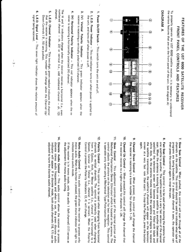
Cirrus Logic CS42518-CQZ User manual

Preliminary Product Information
This document contains information for a new product.
Cirrus Logic reserves the right to modify this product without notice.
1
Copyright
©
Cirrus Logic, Inc. 2004
(All Rights Reserved)
Cirrus Logic, Inc.
http://www.cirrus.com
CS42518
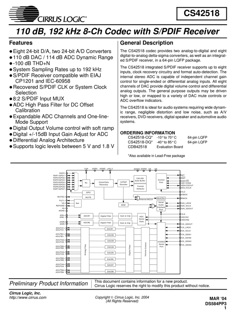
110 dB, 192 kHz 8-Ch Codec with S/PDIF Receiver
Features
Eight 24-bit D/A, two 24-bit A/D Converters
110 dB DAC / 114 dB ADC Dynamic Range
-100 dB THD+N
System Sampling Rates up to 192 kHz
S/PDIF Receiver compatible with EIAJ
CP1201 and IEC-60958
Recovered S/PDIF CLK or System Clock
Selection
8:2 S/PDIF Input MUX
ADC High Pass Filter for DC Offset
Calibration
Expandable ADC Channels and One-line-
Mode Support
Digital Output Volume control with soft ramp
Digital +/-15dB Input Gain Adjust for ADC
Differential Analog Architecture
Supports logic levels between 5 V and 1.8 V
General Description
The CS42518 codec provides two analog-to-digital and eight
digital-to-analog delta-sigma converters, as well as an integrat-
ed S/PDIF receiver, in a 64-pin LQFP package.
The CS42518 integrated S/PDIF receiver supports up to eight
inputs, clock recovery circuitry and format auto-detection. The
internal stereo ADC is capable of independent channel gain
control for single-ended or differential analog inputs. All eight
channels of DAC provide digital volume control and differential
analog outputs. The general purpose outputs may be driven
high or low, or mapped to a variety of DAC mute controls or
ADC overflow indicators.
The CS42518 is ideal for audio systems requiring wide dynam-
ic range, negligible distortion and low noise, such as A/V
receivers, DVD receivers, digital speaker and automotive audio
systems.
ORDERING INFORMATION
CS42518-CQ -10° to 70° C 64-pin LQFP
CS42518-CQZ -10° to 70° C 64-pin LQFP
CS42518-DQZ -40° to 85° C 64-pin LQFP
CDB42518 Evaluation Board
RST
RXP0
RXP1/GPO1
AD0/CS
SCL/CCLK
SDA/CDOUT
AD1/CDIN
VLC
AOUTA1+
AOUTA1-
AOUTB1+
AOUTA3+
AOUTA3-
AOUTA2-
AOUTB2-
AOUTA2+
AOUTB2+
AOUTB1-
AOUTB3+
AOUTB3-
AOUTA4+
AOUTA4-
AOUTB4+
AOUTB4-
AINL+
AINL-
AINR+
AINR-
FILT+
REFGND
VQ Ref
ADC#1
ADC#2
D igit al F ilte r
Digital Filter
G ain & C lip
Gain & Clip CX_SDOUT
ADCIN1
ADCIN2
CX_SCLK
CX_LRCK
CX_SDIN4
CX_SDIN3
CX_SDIN2
CX_SDIN1
VLS
SAI_LRCK
SAI_SCLK
SAI_SDOUT
DGND VD
OMCK
RMCK
LPFLTTXP
INT
Rx Clock/Data
Recovery
S/PDIF
Decoder
DEM
Serial
Audio
Interface
Port
C&U Bit
Data Buffer Control
Port
DAC#1
DAC#2
DAC#3
DAC#4
DAC#5
DAC#6
DAC#7
DAC#8
DigitalFilter
VolumeControl
DGND
RXP2/GPO2
RXP3/GPO3
RXP4/GPO4
RXP5/GPO5
RXP6/GPO6
RXP7/GPO7
VD
MUTEC
GPO
MUTE
AnalogFilter
VARX AGND
ADC
Serial
Data
AGND
VA
Internal MCLK
CODEC
Serial
Port
Mult/Div
Format
Detector
JUL ‘04
DS584PP4

CS42518
2
TABLE OF CONTENTS
1 CHARACTERISTICS AND SPECIFICATIONS ......................................................................... 7
SPECIFIED OPERATING CONDITIONS ................................................................................. 7
ABSOLUTE MAXIMUM RATINGS ........................................................................................... 7
ANALOG INPUT CHARACTERISTICS .................................................................................... 8
A/D DIGITAL FILTER CHARACTERISTICS............................................................................. 9
ANALOG OUTPUT CHARACTERISTICS .............................................................................. 10
D/A DIGITAL FILTER CHARACTERISTICS........................................................................... 11
SWITCHING CHARACTERISTICS ........................................................................................ 12
SWITCHING CHARACTERISTICS - CONTROL PORT - I2C FORMAT................................ 13
SWITCHING CHARACTERISTICS - CONTROL PORT - SPI FORMAT ............................... 14
DC ELECTRICAL CHARACTERISTICS................................................................................. 15
DIGITAL INTERFACE CHARACTERISTICS.......................................................................... 15
2 PIN DESCRIPTIONS ............................................................................................................... 16
3 TYPICAL CONNECTION DIAGRAMS ................................................................................. 19
4 APPLICATIONS ....................................................................................................................... 21
4.1. Overview ......................................................................................................................... 21
4.2. Analog Inputs .................................................................................................................. 21
4.2.1 Line Level Inputs ................................................................................................. 21
4.2.2 High Pass Filter and DC Offset Calibration ......................................................... 22
4.3. Analog Outputs ............................................................................................................... 22
4.3.1 Line Level Outputs and Filtering ......................................................................... 22
4.3.2 Interpolation Filter ............................................................................................... 22
4.3.3 Digital Volume and Mute Control ........................................................................ 23
IMPORTANT NOTICE
"Preliminary" product information describes products that are in production, but for which full characterization data is not yet available. Cirrus Logic,
Inc. and its subsidiaries ("Cirrus") believe that the information contained in this document is accurate and reliable. However, the information is subject
to change without notice and is provided "AS IS" without warranty of any kind (express or implied). Customers are advised to obtain the latest version
of relevant information to verify, before placing orders, that information being relied on is current and complete. All products are sold subject to the
terms and conditions of sale supplied at the time of order acknowledgment, including those pertaining to warranty, patent infringement, and limitation
of liability. No responsibility is assumed by Cirrus for the use of this information, including use of this information as the basis for manufacture or sale
of any items, or for infringement of patents or other rights of third parties. This document is the property of Cirrus and by furnishing this information,
Cirrus grants no license, express or implied under any patents, mask work rights, copyrights, trademarks, trade secrets or other intellectual property
rights. Cirrus owns the copyrights associated with the information contained herein and gives consent for copies to be made of the information only
for use within your organization with respect to Cirrus integrated circuits or other parts of Cirrus. This consent does not extend to other copying such
as copying for general distribution, advertising or promotional purposes, or for creating any work for resale.
An export permit needs to be obtained from the competent authorities of the Japanese Government if any of the products or technologies described
in this material and controlled under the "Foreign Exchange and Foreign Trade Law" is to be exported or taken out of Japan. An export license and/or
quota needs to be obtained from the competent authorities of the Chinese Government if any of the products or technologies described in this material
is subject to the PRC Foreign Trade Law and is to be exported or taken out of the PRC.
CERTAIN APPLICATIONS USING SEMICONDUCTOR PRODUCTS MAY INVOLVE POTENTIAL RISKS OF DEATH, PERSONAL INJURY, OR
SEVERE PROPERTY OR ENVIRONMENTAL DAMAGE ("CRITICAL APPLICATIONS"). CIRRUS PRODUCTS ARE NOT DESIGNED, AUTHO-
RIZED OR WARRANTED FOR USE IN AIRCRAFT SYSTEMS, MILITARY APPLICATIONS, PRODUCTS SURGICALLY IMPLANTED INTO THE
BODY, LIFE SUPPORT PRODUCTS OR OTHER CRITICAL APPLICATIONS (INCLUDING MEDICAL DEVICES, AIRCRAFT SYSTEMS OR COM-
PONENTS AND PERSONAL OR AUTOMOTIVE SAFETY OR SECURITY DEVICES). INCLUSION OF CIRRUS PRODUCTS IN SUCH APPLICA-
TIONS IS UNDERSTOOD TO BE FULLY AT THE CUSTOMER'S RISK AND CIRRUS DISCLAIMS AND MAKES NO WARRANTY, EXPRESS,
STATUTORY OR IMPLIED, INCLUDING THE IMPLIED WARRANTIES OF MERCHANTABILITY AND FITNESS FOR PARTICULAR PURPOSE,
WITH REGARD TO ANY CIRRUS PRODUCT THAT IS USED IN SUCH A MANNER. IF THE CUSTOMER OR CUSTOMER'S CUSTOMER USES
OR PERMITS THE USE OF CIRRUS PRODUCTS IN CRITICAL APPLICATIONS, CUSTOMER AGREES, BY SUCH USE, TO FULLY INDEMNIFY
CIRRUS, ITS OFFICERS, DIRECTORS, EMPLOYEES, DISTRIBUTORS AND OTHER AGENTS FROM ANY AND ALL LIABILITY, INCLUDING
ATTORNEYS' FEES AND COSTS, THAT MAY RESULT FROM OR ARISE IN CONNECTION WITH THESE USES.
AC-3 is a registered trademark of Dolby Laboratories Licensing Corporation. DTS is a registered trademark of the Digital Theater Systems Corporation. I
2
C is
a registered trademark of Philips Semiconductor. Purchase of I
2
C components of Cirrus Logic, Inc., or one of its sublicensed Associated Companies conveys a
license under the Phillips I
2
C Patent Rights to use those components in a standard I
2
C system.
Cirrus Logic, Cirrus, and the Cirrus Logic logo designs are trademarks of Cirrus Logic, Inc. All other brand and product names in this document may
be trademarks or service marks of their respective owners.
Contacting Cirrus Logic Support
For all product questions and inquiries contact a Cirrus Logic Sales Representative.
To find one nearest you go to http://www.cirrus.com/

3
CS42518
4.3.4 ATAPI Specification ............................................................................................ 23
4.4. S/PDIF Receiver ............................................................................................................. 24
4.4.1 8:2 S/PDIF Input Multiplexer ............................................................................... 24
4.4.2 Error Reporting and Hold Function ..................................................................... 24
4.4.3 Channel Status Data Handling ............................................................................ 24
4.4.4 User Data Handling ............................................................................................. 24
4.4.5 Non-Audio Auto-Detection .................................................................................. 24
4.5. Clock Generation ............................................................................................................ 25
4.5.1 PLL and Jitter Attenuation ................................................................................... 25
4.5.2 OMCK System Clock Mode ................................................................................ 26
4.5.3 Master Mode ....................................................................................................... 26
4.5.4 Slave Mode ......................................................................................................... 26
4.6. Digital Interfaces ............................................................................................................. 27
4.6.1 Serial Audio Interface Signals ............................................................................. 27
4.6.2 Serial Audio Interface Formats ........................................................................... 29
4.6.3 ADCIN1/ADCIN2 Serial Data Format ................................................................. 32
4.6.4 One Line Mode(OLM) Configurations ................................................................. 33
4.6.4a OLM Config #1 ..................................................................................... 33
4.6.4b OLM Config #2 ..................................................................................... 34
4.6.4c OLM Config #3 ..................................................................................... 35
4.6.4d OLM Config #4 ..................................................................................... 36
4.6.4e OLM Config #5 ..................................................................................... 37
4.7. Control Port Description and Timing ............................................................................... 38
4.7.1 SPI Mode ............................................................................................................ 38
4.7.2 I2C Mode ............................................................................................................ 39
4.8. Interrupts ........................................................................................................................ 40
4.9. Reset and Power-up ...................................................................................................... 40
4.10. Power Supply, Grounding, and PCB layout .................................................................. 40
5 REGISTER QUICK REFERENCE ........................................................................................... 42
6 REGISTER DESCRIPTION ..................................................................................................... 46
6.1 Memory Address Pointer (MAP)....................................................................................... 46
6.2 Chip I.D. and Revision Register (address 01h) (Read Only)............................................ 46
6.3 Power Control (address 02h)............................................................................................ 47
6.4 Functional Mode (address 03h)........................................................................................ 47
6.5 Interface Formats (address 04h) ...................................................................................... 49
6.6 Misc Control (address 05h) .............................................................................................. 51
6.7 Clock Control (address 06h)............................................................................................. 52
6.8 OMCK/PLL_CLK Ratio (address 07h) (Read Only) ......................................................... 54
6.9 RVCR Status (address 08h) (Read Only)......................................................................... 54
6.10 Burst Preamble PC and PD Bytes (addresses 09h - 0Ch)(Read Only).......................... 55
6.11 Volume Transition Control (address 0Dh) ...................................................................... 56
6.12 Channel Mute (address 0Eh).......................................................................................... 58
6.13 Volume Control (addresses 0Fh, 10h, 11h, 12h, 13h, 14h, 15h, 16h) ........................ 58
6.14 Channel Invert (address 17h) ......................................................................................... 58
6.15 Mixing Control Pair 1 (Channels A1 & B1)(address 18h)
Mixing Control Pair 2 (Channels A2 & B2)(address 19h)
Mixing Control Pair 3 (Channels A3 & B3)(address 1Ah)
Mixing Control Pair 4 (Channels A4 & B4)(address 1Bh) ............................................ 59
6.16 ADC Left Channel Gain (address 1Ch) .......................................................................... 61
6.17 ADC Right Channel Gain (address 1Dh)........................................................................ 61
6.18 Receiver Mode Control (address 1Eh) ........................................................................... 61
6.19 Receiver Mode Control 2 (address 1Fh) ........................................................................ 62
6.20 Interrupt Status (address 20h) (Read Only) ................................................................... 63

CS42518
4
6.21 Interrupt Mask (address 21h).......................................................................................... 64
6.22 Interrupt Mode MSB (address 22h)
Interrupt Mode LSB (address 23h)................................................................................ 64
6.23 Channel Status Data Buffer Control (address 24h) ........................................................ 65
6.24 Receiver Channel Status (address 25h) (Read Only)..................................................... 65
6.25 Receiver Errors (address 26h) (Read Only) ................................................................... 66
6.26 Receiver Errors Mask (address 27h) .............................................................................. 68
6.27 MuteC Pin Control (address 28h) ................................................................................... 68
6.28 RXP/General Purpose Pin Control (addresses 29h to 2Fh) ........................................... 69
6.29 Q-Channel Subcode Bytes 0 to 9 (addresses 30h to 39h) (Read Only) ......................... 70
6.30 C-bit or U-bit Data Buffer (addresses 3Ah to 51h) (Read Only)...................................... 70
7 PARAMETER DEFINITIONS ................................................................................................... 71
8 REFERENCES ......................................................................................................................... 72
9 PACKAGE DIMENSIONS ..................................................................................................... 73
THERMAL CHARACTERISTICS............................................................................................ 73
10 APPENDIX A: EXTERNAL FILTERS .................................................................................... 74
10.1. ADC Input Filter ............................................................................................................ 74
10.2. DAC Output Filter .......................................................................................................... 74
11 APPENDIX B: S/PDIF RECEIVER ........................................................................................ 75
11.1. Error Reporting and Hold Function ............................................................................... 75
11.2 Channel Status Data Handling ....................................................................................... 75
11.2.1 Channel Status Data E Buffer Access .............................................................. 76
11.2.1a One Byte mode .................................................................................. 76
11.2.1b Two Byte mode .................................................................................. 76
11.2.2 Serial Copy Management System (SCMS) ....................................................... 77
11.3. User (U) Data E Buffer Access ..................................................................................... 77
11.3.1 Non-Audio Auto-Detection ................................................................................ 77
11.3.1a Format Detection ................................................................................ 77
12 APPENDIX C: PLL FILTER ................................................................................................... 78
12.1. External Filter Components .......................................................................................... 79
12.1.1 General ............................................................................................................. 79
12.1.2 Jitter Attenuation ............................................................................................... 79
12.1.3 Capacitor Selection ........................................................................................... 80
12.1.4 Circuit Board Layout .......................................................................................... 80
13 APPENDIX D: EXTERNAL AES3/SPDIF/IEC60958 RECEIVER COMPONENTS ............... 81
13.1. AES3 Receiver External Components .......................................................................... 81
14 APPENDIX E: ADC FILTER PLOTS ..................................................................................... 82
15 APPENDIX F: DAC FILTER PLOTS ..................................................................................... 84

5
CS42518
LIST OF FIGURES
Figure 1. Serial Audio Port Master Mode Timing .......................................................................... 12
Figure 2. Serial Audio Port Slave Mode Timing ............................................................................ 12
Figure 3. Control Port Timing - I2C Format................................................................................... 13
Figure 4. Control Port Timing - SPI Format................................................................................... 14
Figure 5. Typical Connection Diagram.......................................................................................... 19
Figure 6. Typical Connection Diagram with PLL........................................................................... 20
Figure 7. Full-Scale Analog Input.................................................................................................. 21
Figure 8. Full-Scale Output ........................................................................................................... 22
Figure 9. ATAPI Block Diagram (x = channel pair 1, 2, 3, 4) ........................................................ 23
Figure 10. CS42518 Clock Generation ......................................................................................... 25
Figure 11. I2S Serial Audio Formats ............................................................................................. 29
Figure 12. Left Justified Serial Audio Formats .............................................................................. 30
Figure 13. Right Justified Serial Audio Formats............................................................................ 30
Figure 14. One Line Mode #1 Serial Audio Format....................................................................... 31
Figure 15. One Line Mode #2 Serial Audio Format....................................................................... 31
Figure 16. ADCIN1/ADCIN2 Serial Audio Format......................................................................... 32
Figure 17. OLM Configuration #1.................................................................................................. 33
Figure 18. OLM Configuration #2.................................................................................................. 34
Figure 19. OLM Configuration #3.................................................................................................. 35
Figure 20. OLM Configuration #4.................................................................................................. 36
Figure 21. OLM Configuration #5.................................................................................................. 37
Figure 22. Control Port Timing in SPI Mode ................................................................................. 38
Figure 23. Control Port Timing, I2C Write..................................................................................... 39
Figure 24. Control Port Timing, I2C Read..................................................................................... 39
Figure 25. Recommended Analog Input Buffer............................................................................. 74
Figure 26. Recommended Analog Output Buffer .......................................................................... 74
Figure 27. Channel Status Data Buffer Structure.......................................................................... 76
Figure 28. PLL Block Diagram ...................................................................................................... 78
Figure 29. Jitter Attenuation Characteristics of PLL...................................................................... 79
Figure 30. Recommended Layout Example.................................................................................. 80
Figure 31. Consumer Input Circuit ................................................................................................ 81
Figure 32. S/PDIF MUX Input Circuit ............................................................................................ 81
Figure 33. TTL/CMOS Input Circuit...............................................................................................81
Figure 34. Single Speed Mode Stopband Rejection ..................................................................... 82
Figure 35. Single Speed Mode Transition Band ........................................................................... 82
Figure 36. Single Speed Mode Transition Band (Detail)............................................................... 82
Figure 37. Single Speed Mode Passband Ripple ......................................................................... 82
Figure 38. Double Speed Mode Stopband Rejection.................................................................... 82
Figure 39. Double Speed Mode Transition Band .......................................................................... 82
Figure 40. Double Speed Mode Transition Band (Detail) ............................................................. 83
Figure 41. Double Speed Mode Passband Ripple ........................................................................ 83
Figure 42. Quad Speed Mode Stopband Rejection ...................................................................... 83
Figure 43. Quad Speed Mode Transition Band............................................................................. 83
Figure 44. Quad Speed Mode Transition Band (Detail) ................................................................ 83
Figure 45. Quad Speed Mode Passband Ripple........................................................................... 83
Figure 46. Single Speed (fast) Stopband Rejection ...................................................................... 84
Figure 47. Single Speed (fast) Transition Band ............................................................................ 84
Figure 48. Single Speed (fast) Transition Band (detail) ................................................................ 84
Figure 49. Single Speed (fast) Passband Ripple .......................................................................... 84
Figure 50. Single Speed (slow) Stopband Rejection..................................................................... 84
Figure 51. Single Speed (slow) Transition Band........................................................................... 84

CS42518
6
Figure 52. Single Speed (slow) Transition Band (detail) ............................................................... 85
Figure 53. Single Speed (slow) Passband Ripple ......................................................................... 85
Figure 54. Double Speed (fast) Stopband Rejection..................................................................... 85
Figure 55. Double Speed (fast) Transition Band ........................................................................... 85
Figure 56. Double Speed (fast) Transition Band (detail) ............................................................... 85
Figure 57. Double Speed (fast) Passband Ripple ......................................................................... 85
Figure 58. Double Speed (slow) Stopband Rejection ................................................................... 86
Figure 59. Double Speed (slow) Transition Band.......................................................................... 86
Figure 60. Double Speed (slow) Transition Band (detail).............................................................. 86
Figure 61. Double Speed (slow) Passband Ripple........................................................................ 86
Figure 62. Quad Speed (fast) Stopband Rejection ....................................................................... 86
Figure 63. Quad Speed (fast) Transition Band.............................................................................. 86
Figure 64. Quad Speed (fast) Transition Band (detail).................................................................. 87
Figure 65. Quad Speed (fast) Passband Ripple............................................................................ 87
Figure 66. Quad Speed (slow) Stopband Rejection ...................................................................... 87
Figure 67. Quad Speed (slow) Transition Band ............................................................................ 87
Figure 68. Quad Speed (slow) Transition Band (detail) ................................................................ 87
Figure 69. Quad Speed (slow) Passband Ripple .......................................................................... 87
LIST OF TABLES
Table 1. Revision History ...................................................................................................................... 6
Table 2. Common OMCK Clock Frequencies...................................................................................... 26
Table 3. Common PLL Output Clock Frequencies ............................................................................. 26
Table 4. Slave Mode Clock Ratios....................................................................................................... 27
Table 5. Serial Audio Port Channel Allocations ................................................................................... 27
Table 6. DAC De-Emphasis................................................................................................................. 48
Table 7. Receiver De-Emphasis .......................................................................................................... 49
Table 8. Digital Interface Formats........................................................................................................ 49
Table 9. ADC One-Line Mode ............................................................................................................. 50
Table 10. DAC One-Line Mode ........................................................................................................... 50
Table 11. RMCK Divider Settings ........................................................................................................ 52
Table 12. OMCK Frequency Settings .................................................................................................. 53
Table 13. Master Clock Source Select ................................................................................................ 53
Table 14. AES Format Detection ......................................................................................................... 54
Table 15. Receiver Clock Frequency Detection .................................................................................. 55
Table 16. Example Digital Volume Settings......................................................................................... 58
Table 17. ATAPI Decode ..................................................................................................................... 60
Table 18. Example ADC Input Gain Settings.......................................................................................61
Table 19. TXP Output Selection .......................................................................................................... 62
Table 20. Receiver Input Selection...................................................................................................... 63
Table 21. Auxiliary Data Width Selection............................................................................................. 66
Table 22. PLL External Component Values.........................................................................................79
Table 1. Revision History
Release Date Changes
A1 December 2002 Advance Release
PP1 August 2003 Preliminary Release
PP2 August 2003 - Added Revision History table.
- Updated registers 6.7.4 and 6.7.5 on p 53.
PP3 March 2004 Correct typo in document title
PP4 July 2004 Add lead free parts

7
CS42518
1 CHARACTERISTICS AND SPECIFICATIONS
(All Min/Max characteristics and specifications are guaranteed over the Specified Operating Conditions. Typical per-
formance characteristics and specifications are derived from measurements taken at nominal supply voltages and
TA= 25° C.)
SPECIFIED OPERATING CONDITIONS (AGND=DGND=0, all voltages with respect to ground;
OMCK=12.288 MHz; Master Mode)
ABSOLUTE MAXIMUM RATINGS (AGND = DGND = 0 V; all voltages with respect to ground.)
WARNING: Operation at or beyond these limits may result in permanent damage to the device. Normal operation is
not guaranteed at these extremes.
Notes: 1. Any pin except supplies. Transient currents of up to ±100 mA on the analog input pins will not cause SCR
latch-up.
2. The maximum over/under voltage is limited by the input current.
Parameter Symbol Min Typ Max Units
DC Power Supply Analog
Digital
Serial Port Interface
Control Port Interface
VA / VARX
VD
VLS
VLC
4.75
3.13
1.8
1.8
5.0
3.3
5.0
5.0
5.25
5.25
5.25
5.25
V
V
V
V
Ambient Operating Temperature (power applied) CS42518-CQ
CS42518-DQ
TA-10
-40
-
-
+70
+85
°C
°C
Parameters Symbol Min Max Units
DC Power Supply Analog
Digital
Serial Port Interface
Control Port Interface
VA / VARX
VD
VLS
VLC
-0.3
-0.3
-0.3
-0.3
6.0
6.0
6.0
6.0
V
V
V
V
Input Current (Note 1) Iin -±10mA
Analog Input Voltage (Note 2) VIN AGND-0.7 VA+0.7 V
Digital Input Voltage Serial Port Interface
(Note 2) Control Port Interface
S/PDIF interface
VIND-S
VIND-C
VIND-SP
-0.3
-0.3
-0.3
VLS+ 0.4
VLC+ 0.4
VARX+0.4
V
V
V
Ambient Operating Temperature(power applied)
CS42518-CQ
CS42518-DQ
TA
TA
-20
-50
+85
+95
°C
°C
Storage Temperature Tstg -65 +150 °C

CS42518
8
ANALOG INPUT CHARACTERISTICS (TA= 25° C; VA =VARX= 5 V, VD = 3.3 V, Logic "0" =
DGND =AGND = 0 V; Logic "1" = VLS = VLC = 5 V; Measurement Bandwidth is 10 Hz to 20 kHz unless otherwise
specified. Full scale input sine wave, 997 Hz.; OMCK = 12.288 MHz; Single speed Mode CX_SCLK = 3.072 MHz;
Double Speed Mode CX_SCLK = 6.144 MHz; Quad Speed Mode CX_SCLK = 12.288 MHz.)
Parameter Symbol
CS42518-CQ
Min Typ Max
CS42518-DQ
Min Typ Max Unit
Single Speed Mode (Fs=48 kHz)
Dynamic Range A-weighted
unweighted
108
105
114
111
-
-
106
103
114
111
-
-
dB
dB
Total Harmonic Distortion + Noise
(Note 3) -1 dB
-20 dB
-60 dB
THD+N
-
-
-
-100
-91
-51
-94
-
-
-
-
-
-100
-91
-51
-92
-
-
dB
dB
dB
Double Speed Mode (Fs=96 kHz)
Dynamic Range A-weighted
unweighted
40 kHz bandwidth unweighted
108
105
-
114
111
108
-
-
-
106
103
-
114
111
108
-
-
-
dB
dB
dB
Total Harmonic Distortion + Noise
(Note 3) -1 dB
-20 dB
-60 dB
40 kHz bandwidth -1 dB
THD+N
-
-
-
-
-100
-91
-51
-97
-94
-
-
-
-
-
-
-
-100
-91
-51
-97
-92
-
-
-
dB
dB
dB
dB
Quad Speed Mode (Fs=192 kHz)
Dynamic Range A-weighted
unweighted
40 kHz bandwidth unweighted
108
105
-
114
111
108
-
-
-
106
103
-
114
111
108
-
-
-
dB
dB
dB
Total Harmonic Distortion + Noise
(Note 3) -1 dB
-20 dB
-60 dB
40 kHz bandwidth -1 dB
THD+N
-
-
-
-
-100
-91
-51
-97
-94
-
-
-
-
-
-
-
-100
-91
-51
-97
-92
-
-
-
dB
dB
dB
dB
Dynamic Performance for All Modes
Interchannel Isolation - 110 - - 110 - dB
Interchannel Phase Deviation - 0.0001 - - 0.0001 - Degree
DC Accuracy
Interchannel Gain Mismatch - 0.1 - - 0.1 - dB
Gain Drift - +/-100 - - +/-100 - ppm/°C
Offset Error HPF_FREEZE enabled
HPF_FREEZE disabled
-
-
0
100
-
-
-
-
0
100
-
-
LSB
LSB
Analog Input
Full-scale Differential Input Voltage 1.05VA 1.10VA 1.16VA 0.99VA 1.10VA 1.21VA Vpp
Input Impedance(differential) (Note
4)
37 - - 37 - - kΩ
Common Mode Rejection Ratio CMRR - 82 - - 82 - dB
VQ Nominal Voltage
Output Impedance
Maximum allowable DC current
-
-
-
2.7
50
0.01
-
-
-
-
-
-
2.7
50
0.01
-
-
-
V
kΩ
mA

9
CS42518
Notes: 3. Referred to the typical full-scale voltage.
4. Measured between AIN+ and AIN-
A/D DIGITAL FILTER CHARACTERISTICS
Notes: 5. The filter frequency response scales precisely with Fs.
6. Response shown is for Fs equal to 48 kHz. Filter characteristics scale with Fs.
FILT+ Nominal Voltage
Output Impedance
Maximum allowable DC current
-
-
-
5.0
35
0.01
-
-
-
-
-
-
5.0
35
0.01
-
-
-
V
kΩ
mA
Parameter Symbol Min Typ Max Unit
Single Speed Mode (2 to 50 kHz sample rates)
Passband (-0.1 dB) (Note 5) 0 - 0.47 Fs
Passband Ripple - - ±0.035 dB
Stopband (Note 5) 0.58 - - Fs
Stopband Attenuation -95 - - dB
Total Group Delay (Fs = Output Sample Rate) tgd -12/Fs- s
Group Delay Variation vs. Frequency ∆tgd --0.0µs
Double Speed Mode (50 to 100 kHz sample rates)
Passband (-0.1 dB) (Note 5) 0 - 0.45 Fs
Passband Ripple - - ±0.035 dB
Stopband (Note 5) 0.68 - - Fs
Stopband Attenuation -92 - - dB
Total Group Delay (Fs = Output Sample Rate) tgd -9/Fs- s
Group Delay Variation vs. Frequency ∆tgd --0.0µs
Quad Speed Mode (100 to 192 kHz sample rates)
Passband (-0.1 dB) (Note 5) 0 - 0.24 Fs
Passband Ripple - - ±0.035 dB
Stopband (Note 5) 0.78 - - Fs
Stopband Attenuation -97 - - dB
Total Group Delay (Fs = Output Sample Rate) tgd -5/Fs- s
Group Delay Variation vs. Frequency ∆tgd --0.0µs
High Pass Filter Characteristics
Frequency Response -3.0 dB
-0.13 dB (Note 6)
-1
20
-
-
Hz
Hz
Phase Deviation @ 20 Hz (Note 6) - 10 - Deg
Passband Ripple - - 0 dB
Filter Setting Time - 105/Fs - s

CS42518
10
ANALOG OUTPUT CHARACTERISTICS (TA= 25° C; VA =VARX= 5 V, VD = 3.3 V, Logic "0" =
DGND =AGND = 0 V; Logic "1" = VLS = VLC = 5V; Measurement Bandwidth 10 Hz to 20 kHz unless otherwise
specified.; Full scale output 997 Hz sine wave, Test load RL= 3 kΩ, CL= 30 pF; OMCK = 12.288 MHz; Single
speed Mode, CX_SCLK = 3.072 MHz; Double Speed Mode, CX_SCLK = 6.144 MHz; Quad Speed Mode,
CX_SCLK = 12.288 MHz.)
Notes: 7. One-half LSB of triangular PDF dither is added to data.
8. Performance limited by 16-bit quantization noise.
Parameter Symbol
CS42518-CQ
Min Typ Max
CS42518-DQ
Min Typ Max Unit
Dynamic performance for all modes
Dynamic Range(Note 7)
24-bit A-Weighted
unweighted
16-bit A-Weighted
(Note 8) unweighted
104
101
-
-
110
107
97
94
-
-
-
-
102
99
-
-
110
107
97
94
-
-
-
-
dB
dB
dB
dB
Total Harmonic Distortion + Noise
24-bit 0 dB
-20 dB
-60 dB
16-bit 0 dB
(Note 8) -20 dB
-60 dB
THD+N
-
-
-
-
-
-
-100
-91
-51
-94
-74
-34
-94
-
-
-
-
-
-
-
-
-
-
-100
-91
-51
-94
-74
-34
-92
-
-
-
-
-
dB
dB
dB
dB
dB
dB
Idle Channel Noise/Signal-to-noise
ratio (A-Weighted)
-110- -110 -dB
Interchannel Isolation (1 kHz) - 90 - - 90 - dB
Analog Output Characteristics for all modes
Full Scale Differential Output .89VA .94VA .99VA .84VA .94VA 1.04VA Vpp
Interchannel Gain Mismatch - 0.1 - - 0.1 - dB
Gain Drift - 100 - - 100 - ppm/°C
Output Impedance ZOUT - 100 - - 100 - Ω
AC-Load Resistance RL3- -3- -kΩ
Load Capacitance CL- - 30 - - 30 pF

11
CS42518
D/A DIGITAL FILTER CHARACTERISTICS
Notes: 9. Response is clock dependent and will scale with Fs. Note that the response plots (Figures 46 to 69) have
been normalized to Fs and can be de-normalized by multiplying the X-axis scale by Fs.
10. Single and Double Speed Mode Measurement Bandwidth is from stopband to 3 Fs.
Quad Speed Mode Measurement Bandwidth is from stopband to 1.34 Fs.
11. De-emphasis is available only in Single Speed Mode.
Parameter
Fast Roll-Off Slow Roll-Off
UnitMin Typ Max Min Typ Max
Combined Digital and On-chip Analog Filter Response - Single Speed Mode - 48 kHz
Passband (Note 9) to -0.01 dB corner
to -3 dB corner
0
0
-
-
0.4535
0.4998
0
0
-
-
0.4166
0.4998
Fs
Fs
Frequency Response 10 Hz to 20 kHz -0.01 - +0.01 -0.01 - +0.01 dB
StopBand 0.5465 - - 0.5834 - - Fs
StopBand Attenuation (Note 10) 90 - - 64 - - dB
Group Delay - 12/Fs - - 6.5/Fs - s
Passband Group Delay Deviation 0 - 20 kHz - - ±0.41/Fs - ±0.14/Fs s
De-emphasis Error (Note 11) Fs = 32 kHz
(Relative to 1 kHz) Fs = 44.1 kHz
Fs = 48 kHz
-
-
-
-
-
-
±0.23
±0.14
±0.09
-
-
-
-
-
-
±0.23
±0.14
±0.09
dB
dB
dB
Combined Digital and On-chip Analog Filter Response - Double Speed Mode - 96 kHz
Passband (Note 9) to -0.01 dB corner
to -3 dB corner
0
0
-
-
0.4166
0.4998
0
0
-
-
0.2083
0.4998
Fs
Fs
Frequency Response 10 Hz to 20 kHz -0.01 - 0.01 -0.01 - 0.01 dB
StopBand 0.5834 - - 0.7917 - - Fs
StopBand Attenuation (Note 10) 80 - - 70 - - dB
Group Delay - 4.6/Fs - - 3.9/Fs - s
Passband Group Delay Deviation 0 - 20 kHz - - ±0.03/Fs - ±0.01/Fs s
Combined Digital and On-chip Analog Filter Response - Quad Speed Mode - 192 kHz
Passband (Note 9) to -0.01 dB corner
to -3 dB corner
0
0
-
-
0.1046
0.4897
0
0
-
-
0.1042
0.4813
Fs
Fs
Frequency Response 10 Hz to 20 kHz -0.01 - 0.01 -0.01 - 0.01 dB
StopBand 0.6355 - - 0.8683 - - Fs
StopBand Attenuation (Note 10) 90 - - 75 - - dB
Group Delay - 4.7/Fs - - 4.2/Fs - s
Passband Group Delay Deviation 0 - 20 kHz - - ±0.01/Fs - ±0.01/Fs s

CS42518
12
SWITCHING CHARACTERISTICS (For CQ, TA= -10 to +70° C; For DQ, TA= -40 to +85° C;
VA=VARX = 5 V, VD =VLC= 3.3 V, VLS = 1.8 V to 5.25 V; Inputs: Logic 0 = DGND, Logic 1 = VLS, CL= 30 pF)
Notes: 12. After powering up the CS42518, RST should be held low after the power supplies and clocks are settled.
13. See Table 2 on page 26 for suggested OMCK frequencies
14. Limit the loading on RMCK to 1 CMOS load if operating above 24.576 MHz.
15. Not valid when RMCK_DIV in “Clock Control (address 06h)” on page 52 is set to Multiply by 2.
Parameters Symbol Min Typ Max Units
RST pin Low Pulse Width (Note 12) 1 - - ms
PLL Clock Recovery Sample Rate Range 30 - 200 kHz
RMCK output jitter (Note 14) - 200 - ps RMS
RMCK output duty cycle (Note 15) 45 50 55 %
OMCK Duty Cycle (Note 13) 40 50 60 %
CX_SCLK, SAI_SCLK Duty Cycle 45 50 55 %
CX_LRCK, SAI_LRCK Duty Cycle 45 50 55 %
Master Mode
RMCK to CX_SCLK, SAI_SCLK active edge delay tsmd 0-15ns
RMCK to CX_LRCK, SAI_LRCK delay tlmd 0-15ns
Slave Mode
CX_SCLK, SAI_SCLK Falling Edge to CX_SDOUT,
SAI_SDOUT Output Valid
tdpd -50ns
CX_LRCK, SAI_LRCK Edge to MSB Valid tlrpd -20ns
CX_SDIN Setup Time Before CX_SCLK Rising Edge tds -10ns
CX_SDIN Hold Time After CX_SCLK Rising Edge tdh -30ns
CX_SCLK, SAI_SCLK High Time tsckh 20 - - ns
CX_SCLK, SAI_SCLK Low Time tsckl 20 - - ns
CX_SCLK, SAI_SCLK falling to CX_LRCK,
SAI_LRCK Edge
tlrck -25 - +25 ns
CX_SCLK
SAI_SCLK
(output)
RMCK
tsmd
tlmd
CX_LRCK
SAI_LRCK
(output)
sckh sckl
t
t
MSB MSB-1
tdpd
CX_SDOUT
SAI_SDOUT
CX_SDINx
dh
t
ds
t
lrpd
t
lrck
t
CX_SCLK
SAI_SCLK
(input)
CX_LRCK
SAI_LRCK
(input)
Figure 1. Serial Audio Port Master Mode Timing Figure 2. Serial Audio Port Slave Mode Timing

13
CS42518
SWITCHING CHARACTERISTICS - CONTROL PORT - I2C FORMAT (For CQ, TA
= -10 to +70° C; For DQ, TA= -40 to +85° C; VA=VARX = 5 V, VD =VLS= 3.3 V; VLC = 1.8 V to 5.25 V; Inputs:
Logic 0 = DGND, Logic 1 = VLC, CL=30pF)
Notes: 16. Data must be held for sufficient time to bridge the transition time, tfc, of SCL.
17. The acknowledge delay is based on MCLK and can limit the maximum transaction speed.
18. for Single-Speed Mode, for Double-Speed Mode, for Quad-Speed Mode
Parameter Symbol Min Max Unit
SCL Clock Frequency fscl - 100 kHz
RST Rising Edge to Start tirs 500 - ns
Bus Free Time Between Transmissions tbuf 4.7 - µs
Start Condition Hold Time (prior to first clock pulse) thdst 4.0 - µs
Clock Low time tlow 4.7 - µs
Clock High Time thigh 4.0 - µs
Setup Time for Repeated Start Condition tsust 4.7 - µs
SDA Hold Time from SCL Falling (Note 16) thdd 0-µs
SDA Setup time to SCL Rising tsud 250 - ns
Rise Time of SCL and SDA trc -1µs
Fall Time SCL and SDA tfc - 300 ns
Setup Time for Stop Condition tsusp 4.7 - µs
Acknowledge Delay from SCL Falling (Note 17) tack - (Note 18) ns
15
256 Fs×
---------------------15
128 F s×
---------------------15
64 Fs×
------------------
tbuf thdst
tlow thdd
thigh
tsud
Stop Start
SDA
SCL
tirs
RST
thdst
trc
tfc
tsust
tsus
p
Start Stop
Repeated
trd tfd
tack
Figure 3. Control Port Timing - I2C Format

CS42518
14
SWITCHING CHARACTERISTICS - CONTROL PORT - SPI FORMAT
(For CQ, TA= -10 to +70° C; For DQ, TA= -40 to +85° C; VA=VARX = 5 V, VD =VLS= 3.3 V; VLC = 1.8 V to 5.25 V;
Inputs: Logic 0 = DGND, Logic 1 = VLC, CL=30pF)
Notes: 19. If Fs is lower than 46.875 kHz, the maximum CCLK frequency should be less than 128 Fs. This is
dictated by the timing requirements necessary to access the Channel Status and User Bit buffer
memory. Access to the control register file can be carried out at the full 6 MHz rate. The minimum
allowable input sample rate is 8 kHz, so choosing CCLK to be less than or equal to 1.024 MHz should
be safe for all possible conditions.
20. Data must be held for sufficient time to bridge the transition time of CCLK.
21. For fsck <1 MHz.
Parameter Symbol Min Typ Max Units
CCLK Clock Frequency (Note 19) fsck 0-6.0MHz
CS High Time Between Transmissions tcsh 1.0 - - µs
CS Falling to CCLK Edge tcss 20 - - ns
CCLK Low Time tscl 66 - - ns
CCLK High Time tsch 66 - - ns
CDIN to CCLK Rising Setup Time tdsu 40 - - ns
CCLK Rising to DATA Hold Time (Note 20) tdh 15 - - ns
CCLK Falling to CDOUT Stable tpd - - 50 ns
Rise Time of CDOUT tr1 - - 25 ns
Fall Time of CDOUT tf1 - - 25 ns
Rise Time of CCLK and CDIN (Note 21) tr2 - - 100 ns
Fall Time of CCLK and CDIN (Note 21) tf2 - - 100 ns
tr2 tf2
tdsu tdh
tsch
tscl
CS
CCLK
CDIN
tcss
tpd
CDOUT
tcsh
Figure 4. Control Port Timing - SPI Format

15
CS42518
DC ELECTRICAL CHARACTERISTICS (TA= 25° C; AGND=DGND=0, all voltages with respect
to ground; OMCK=12.288 MHz; Master Mode)
Notes: 22. Current consumption increases with increasing FS and increasing OMCK. Max values are based on
highest FS and highest OMCK. Variance between speed modes is negligible.
23. ILC measured with no external loading on the SDA pin.
24. Power down mode is defined as RST pin = Low with all clock and data lines held static.
25. Valid with the recommended capacitor values on FILT+ and VQ as shown in Figure 5.
DIGITAL INTERFACE CHARACTERISTICS (For CQ, TA= +25° C; For DQ, TA= -40 to +85° C)
Notes: 26. Serial Port signals include: RMCK, OMCK, SAI_SCLK, SAI_LRCK, SAI_SDOUT, CX_SCLK,
C X _ L R C K , C X _ S D O U T , C X _ S D I N 1 - 4 A D C I N 1 / 2
Control Port signals include: SCL/CCLK, SDA/CDOUT, AD0/CS, AD1/CDIN, INT, RST
S/PDIF-GPO Interface signals include: RXP0, RXP/GPO[1:7]
27. When operating RMCK above 24.576 MHz, limit the loading on the signal to 1 CMOS load.
Parameter Symbol Min Typ Max Units
Power Supply Current normal operation, VA = VARX = 5 V
(Note 22) VD = 5 V
VD = 3.3 V
Interface current, VLC=5 V (Note 23)
VLS=5 V
power-down state (all supplies) (Note 24)
IA
ID
ID
ILC
ILS
Ipd
-
-
-
-
-
-
90
150
100
250
250
250
-
-
-
-
-
-
mA
mA
mA
µA
µA
µA
Power Consumption (Note 22)
VA=VARX=5 V, VD=VLS=VLC=3.3 V normal operation
power-down (Note 24)
VA=VARX=5 V, VD=VLS=VLC=5 V normal operation
power-down (Note 24)
-
-
-
-
780
1.25
950
1.25
850
-
1050
-
mW
mW
mW
mW
Power Supply Rejection Ratio (Note 25) (1 kHz)
(60 Hz)
PSRR -
-
60
40
-
-
dB
dB
Parameters (Note 26) Symbol Min Typ Max Units
High-Level Input Voltage Serial Port
Control Port VIH
0.7xVLS
0.7xVLC
-
-
-
-
V
V
Low-Level Input Voltage Serial Port
Control Port VIL
-
-
-
-
0.2xVLS
0.2xVLC
V
V
High-Level Output Voltage at Io=2 mA (Note 27)Serial Port
Control Port
MUTEC, GPOx
TXP
VOH
VLS-1.0
VLC-1.0
VA-1.0
VD-1.0
-
-
-
-
-
-
-
-
V
V
V
V
Low-Level Output Voltage at Io=2 mA (Note 27)
Serial Port, Control Port, MUTEC, GPOx,TXP VOL --0.4V
Input Sensitivity, RXP[7:0] VTH - 150 200 mVpp
Input Leakage Current Iin --±10µA
Input Capacitance - 8 - pF
MUTEC Drive Current - 3 - mA

CS42518
16
2 PIN DESCRIPTIONS
Pin Name #Pin Description
CX_SDIN1
CX_SDIN2
CX_SDIN3
CX_SDIN4
1
64
63
62
Codec Serial Audio Data Input (
Input
) - Input for two’s complement serial audio data.
CX_SCLK 2CODEC Serial Clock
(Input/Output)
- Serial clock for the CODEC serial audio interface.
CX_LRCK 3CODEC Left Right Clock (
Input
/
Output
) - Determines which channel, Left or Right, is currently active on
the CODEC serial audio data line.
VD 4
51
Digital Power (
Input
) - Positive power supply for the digital section.
DGND 5
52
Digital Ground (
Input
) - Ground reference. Should be connected to digital ground.
VLC 6Control Port Power (
Input
) - Determines the required signal level for the control port.
SCL/CCLK 7Serial Control Port Clock (
Input
) - Serial clock for the serial control port. Requires an external pull-up
resistor to the logic interface voltage in I2C mode as shown in the Typical Connection Diagram.
SDA/CDOUT 8Serial Control Data (
Input/Output
) - SDA is a data I/O line in I2C mode and requires an external pull-up
resistor to the logic interface voltage, as shown in the Typical Connection Diagram. CDOUT is the output
data line for the control port interface in SPI mode.
AD1/CDIN 9Address Bit 1 (I2C)/Serial Control Data (SPI) (
Input
) - AD1 is a chip address pin in I2C mode; CDIN is
the input data line for the control port interface in SPI mode.
1
2
3
4
5
6
7
8
9
10
11
12
13
14
15
16
17 18 19 20 21 22 23 24 25 26 27 28 29 30 31 32
64 63 62 61 60 59 58 57 56 55 54 53 52 51 50 49
48
47
46
45
44
43
42
41
40
39
38
37
36
35
34
33
CX_SDIN1
SAI_SCLK
SAI_LRCK
VD
DGND
VLC
SCL/CCLK
SDA/CDOUT
AD1/CDIN
AD0/CS
INT
RST
AINR-
AINR+
AINL+
AINL-
VQ
FILT+
REFGND
AOUTB4-
AOUTB4+
AOUTA4+
AOUTA4-
VA
AGND
AOUTB3-
AOUTB3+
AOUTA3+
AOUTA3-
AOUTB2-
AOUTB2+
AOUTA2+
AOUTA2-
AOUTB1-
AOUTB1+
AOUTA1+
AOUTA1-
MUTEC
AGND
VARX
RXP7/GPO7
RXP6/GPO6
RXP5/GPO5
RXP4/GPO4
RXP3/GPO3
RXP2/GPO2
RXP1/GPO1
LPFLT
RXP0
TXP
VD
DGND
VLS
SAI_SDOU
T
RMCK
CX_SDOUT
ADCIN2
ADCIN1
OMCK
CX_LRCK
CX_SCLK
CX_SDIN4
CX_SDIN3
CX_SDIN2
CS42518

17
CS42518
AD0/CS 10 Address Bit 0 (I2C)/Control Port Chip Select (SPI)
(Input
)- AD0 is a chip address pin in I2C mode; CS
is the chip select signal in SPI mode.
INT 11 Interrupt
(Output
) - The CS42518 will generate an interrupt condition as per the Interrupt Mask register.
See “Interrupts” on page 40 for more details.
RST 12 Reset (
Input
) - The device enters a low power mode and all internal registers are reset to their default
settings when low.
AINR-
AINR+
13
14
Differential Right Channel Analog Input (
Input
) - Signals are presented differentially to the delta-sigma
modulators via the AINR+/- pins.
AINL+
AINL-
15
16
Differential Left Channel Analog Input (
Input
) - Signals are presented differentially to the delta-sigma
modulators via the AINL+/- pins.
VQ 17 Quiescent Voltage (
Output
) - Filter connection for internal quiescent reference voltage.
FILT+ 18 Positive Voltage Reference (
Output
) - Positive reference voltage for the internal sampling circuits.
REFGND 19 Reference Ground (
Input
) - Ground reference for the internal sampling circuits.
AOUTA1 +,-
AOUTB1 +,-
AOUTA2 +,-
AOUTB2 +,-
AOUTA3 +,-
AOUTB3 +,-
AOUTA4 +,-
AOUTB4 +,-
36,37
35,34
32,33
31,30
28,29
27,26
22,23
21,20
Differential Analog Output (
Output
) - The full-scale differential analog output level is specified in the
Analog Characteristics specification table.
VA
VARX
24
41
Analog Power (
Input
) - Positive power supply for the analog section.
AGND 25
40
Analog Ground (
Input
) - Ground reference. Should be connected to analog ground.
MUTEC 38 Mute Control (
Output
) - The Mute Control pin outputs high impedance following an initial power-on con-
dition or whenever the PDN bit is set to a ‘1’, forcing the codec into power-down mode. The signal will
remain in a high impedance state as long as the part is in power-down mode. The Mute Control pin goes
to the selected “active” state during reset, muting, or if the master clock to left/right clock frequency ratio
is incorrect. This pin is intended to be used as a control for external mute circuits to prevent the clicks
and pops that can occur in any single supply system. The use of external mute circuits are not manda-
tory but may be desired for designs requiring the absolute minimum in extraneous clicks and pops.
LPFLT 39 PLL Loop Filter (
Output
) - An RC network should be connected between this pin and ground.
RXP7/GPO7
RXP6/GPO6
RXP5/GPO5
RXP4/GPO4
RXP3/GPO3
RXP2/GPO2
RXP1/GPO1
42
43
44
45
46
47
48
S/PDIF Receiver Input/ General Purpose Output (
Input/Output
) - Receiver inputs for S/PDIF encoded
data. The CS42518 has an internal 8:2 multiplexer to select the active receiver port, according to the
Receiver Mode Control 2 register. These pins can also be configured as general purpose output pins,
ADC Overflow indicators or Mute Control outputs according to the RXP/General Purpose Pin Control
registers.
RXP0 49 S/PDIF Receiver Input (
Input
) - Dedicated receiver input for S/PDIF encoded data.
TXP 50 S/PDIF Transmitter Output (
Output
) - S/PDIF encoded data output, mapped directly from one of the
receiver inputs as indicated by the Receiver Mode Control 2 register.
VLS 53 Serial Port Interface Power (
Input
) - Determines the required signal level for the serial port interfaces.
SAI_SDOUT 54 Serial Audio Interface Serial Data Output (
Output
) - Output for two’s complement serial audio PCM
data from the S/PDIF incoming stream. This pin can also be configured to transmit the output of the inter-
nal and external ADCs.
RMCK 55 Recovered Master Clock (
Output
) - Recovered master clock output from the External Clock Reference
(OMCK, pin 59) or the PLL which is locked to the incoming S/PDIF stream or CX_LRCK.

CS42518
18
CX_SDOUT 56 CODEC Serial Data Output (
Output
) - Output for two’s complement serial audio data from the internal
and external ADCs.
ADCIN1
ADCIN2
58
57
External ADC Serial Input (
Input
) - The CS42518 provides for up to two external stereo analog to digital
converter inputs to provide a maximum of six channels on one serial data output line when the CS42518
is placed in One Line mode.
OMCK 59 External Reference Clock (
Input
) - External clock reference that must be within the ranges specified in
the register “OMCK Frequency (OMCK Freqx)” on page 53.
SAI_LRCK 60 Serial Audio Interface Left/Right Clock (
Input
/
Output
) - Determines which channel, Left or Right, is
currently active on the serial audio data line.
SAI_SCLK 61 Serial Audio Interface Serial Clock
(Input/Output)
- Serial clock for the Serial Audio Interface.

19
CS42518
3 TYPICAL CONNECTION DIAGRAMS
VD
AOUTA1+
24
0.1 µF +10 µF
100 µF
0.1 µF
+
+
17
18
VQ
FILT+
36
37
0.1 µF
4.7 µF
VA
+
10 µF
51
AOUTA1-
AOUTB1+ 35
34
AOUTB1-
AOUTA2+ 32
33
AOUTA2-
AOUTB2+ 31
30
AOUTB2-
AOUTA3+ 28
29
AOUTA3-
AOUTB3+ 27
26
AOUTB3-
AOUTA4+ 22
23
AOUTA4-
AOUTB4+ 21
20
AOUTB4-
MUTEC 38
25
DGND DGND
5
REFGND 19
41
4
VAVD
0.1 µF
AGNDAGND
52 40
LPFLT 39
AINL+
AINL-
AINR+
AINR-
15
16
14
13
Connect DGND and A GND at single point near Codec
0.01 µF
0.1 µF +10 µF
+5 V
0.01 µF
0.01 µF
+3.3 V to +5 V
+
10 µF 0.1 µF 0.01 µF
VLS
0.1 µF
+2.5 V
to +5 V
53
VLC
0.1 µF
+1.8 V
to +5 V
6
3
60
59
62
1
64
61
2
63
8
7SCL/CCLK
SDA/CDOUT
AD1/CDIN
RST
12
9
OMCK
CX_SDIN1
SAI_LRCK
SAI_SCLK
CX_SDIN3
CX_SDIN2
CX_SDIN4
CX_LRCK
CX_SCLK
AD0/CS
10
INT
11
Digital Audio
Processor
Micro-
Co ntroller
55 RMCK
58 ADCIN1
57 ADCIN2
CS5361
A/D Converter
CS5361
A/D Converter
56 CX_SDOUT
54 SAI_SDOUT
48
46
49
44
45
47
RXP0
RXP1/GPO1
S/PDIF
Interface
50 TXP
Driver
Up to 8
Sources
43
RXP2/GPO2
RXP3/GPO3
RXP4/GPO4
RXP5/GPO5
RXP6/GPO6
RXP7/GPO7
42
OSC
Analog Output Buffer 2
and
Mute Circuit (optional)
Analog Output Buffer 2
and
Mute Circuit (optional)
Analog Output Buffer 2
and
Mute Circuit (optional)
Analog Output Buffer 2
and
Mute Circuit (optional)
Analog Output Buffer 2
and
Mute Circuit (optional)
Analog Output Buffer 2
and
Mute Circuit (optional)
Analog Output Buffer 2
and
Mute Circuit (optional)
Analog Output Buffer 2
and
Mute Circuit (optional)
Mute
Drive
(optional)
+VA
*
* Pull up or down as
required on startup if the
Mute Control is used.
*
2700 pF*
2700 pF*
Left Analog Input
Right Analog Inpu
Analog
Input
Buffer 1
Analog
Input
Buffer 1
CFILT 3
RFILT 3
CRIP 3
2 kΩ2 kΩ
** **
** Resistors are required for
I2C control port operation
1. See the ADC Input Filter section in the Appendix.
2. See the DAC Output Filter section in the Appendix.
3. See the PLL Filter section in the Appendix.
Figure 5. Typical Connection Diagram
CS42518

CS42518
20
VD
AOUTA1+
24
0.1 µF +10 µF
100 µF
0.1 µF
+
+
17
18
VQ
FILT+
36
37
0.1 µF
4.7 µF
VA
+
10 µF
51
AOUTA1-
AOUTB1+ 35
34
AOUTB1-
AOUTA2+ 32
33
AOUTA2-
AOUTB2+ 31
30
AOUTB2-
AOUTA3+ 28
29
AOUTA3-
AOUTB3+ 27
26
AOUTB3-
AOUTA4+ 22
23
AOUTA4-
AOUTB4+ 21
20
AOUTB4-
MUTEC 38
25
DGND DGND
5
REFGND 19
41
4
VAVD
0.1 µF
AGNDAGND
52 40
LPFLT 39
AINL+
AINL-
AINR+
AINR-
15
16
14
13
Connect DGND and AGND at single point near Codec
0.01 µF
0.1 µF +10 µF
+5 V
0.01 µF
0.01 µF
+3.3 V to +5 V
+
10 µF 0.1 µF 0.01 µF
VLS
VLC
SCL/CCLK
SDA/CDOUT
AD1/CDIN
RST
OMCK
CX_SDIN1
SAI_LRCK
SAI_SCLK
CX_SDIN3
CX_SDIN2
CX_SDIN4
CX_LRCK
CX_SCLK
AD0/CS
INT
RMCK
ADCIN1
ADCIN2
CX_SDOUT
SAI_SDOUT
48
46
49
44
45
47
RXP0
RXP1/GPO1
S/PDIF
Interface
50 TXP
Driver
Up to 8
Sources
43
RXP2/GPO2
RXP3/GPO3
RXP4/GPO4
RXP5/GPO5
RXP6/GPO6
RXP7/GPO7
42
0.1 µF
+1.8 V to +5.0 V 53
0.1 µF
6
3
60
59
62
1
64
61
2
63
8
7
12
9
10
11
DVD
Processor
55
58
57
56
27 MHz
54
Analog Output Buffer 2
and
Mute Circuit (optional)
Analog Output Buffer 2
and
Mute Circuit (optional)
Analog Output Buffer 2
and
Mute Circuit (optional)
Analog Output Buffer 2
and
Mute Circuit (optional)
Analog Output Buffer 2
and
Mute Circuit (optional)
Analog Output Buffer 2
and
Mute Circuit (optional)
Analog Output Buffer 2
and
Mute Circuit (optional)
Analog Output Buffer 2
and
Mute Circuit (optional)
Mute
Drive
(optional)
*
*
2700 pF*
2700 pF*
Left Analog Input
Right Analog Input
Analog
Input
Buffer 1
Analog
Input
Buffer 1
CFILT 3
RFILT 3
CRIP 3
2 kΩ2 kΩ
** **
* Pull up or down as
required on startup if the
Mute Control is used.
+VA
** Resistors are required for
I2C control port operation
1. See the ADC Input Filter section in the Appendix.
2. See the DAC Output Filter section in the Appendix.
3. See the PLL Filter section in the Appendix.
Figure 6. Typical Connection Diagram with PLL
CS42518
This manual suits for next models
3
Table of contents
Other Cirrus Logic Receiver manuals
Popular Receiver manuals by other brands

Onkyo
Onkyo NC 500 - NetTune Receiver instruction manual

EZCast
EZCast Mini Box quick start guide
Di-soric
Di-soric SLB2 Quick installation guide
Express
Express EC8500T Hybrid DVB-T Quick install manual
Pioneer
Pioneer VSX-1020-K Operating insructions
Berker
Berker Radio Touch 2880 Series Operation and installation instructions
Rohde & Schwarz
Rohde & Schwarz ESRP EMI Getting started
Marantz
Marantz RX101 user guide
GAMA Electronics
GAMA Electronics RFR12VPRWP instruction manual

Philips
Philips MRD130 Service manual
Yamaha
Yamaha HTR-6260 owner's manual
Dual Electronics Corporation
Dual Electronics Corporation XVMBT279 Installation & owner's manual
