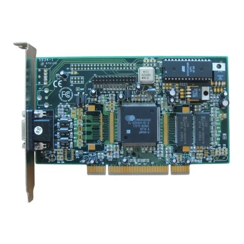
Cirrus Logic Crystal CS8427 Series User manual

Preliminary Product Information This document contains information for a new product.
Cirrus Logic reserves the right to modify this product without notice.
1
Copyright Cirrus Logic, Inc. 1999
(All Rights Reserved)
P.O. Box 17847, Austin, Texas 78760
(512) 445 7222 FAX: (512) 445 7581
http://www.cirrus.com
CS8427
96 kHz Digital Audio Interface Transceiver
Features
lComplete EIAJ CP1201, IEC-60958, AES3,
S/PDIF compatible transceiver
l+3V to +5V Digital Supply
lFlexible 3-wire serial digital I/O ports
lAdjustable sample rate up to 96 kHz
lLow jitter clock recovery
lPin and microcontroller read/write access to
Channel Status and User data
lMicrocontroller and stand-alone modes
lDifferential cable driver & receiver
lOn-chipChannelStatusandUserdatabuffer
memory provides block reads & writes
lOMCK System Clock Mode
lDecodes Audio CD Q sub-code
General Description
The CS8427 is a stereo digital audio transceiver with
AES3 and serial digital audio inputs, AES3 and serial
digital audio outputs, along with comprehensive control
ability via a 4-wire microcontroller port. Channel status
and user data are assembled in block sized buffers,
making read/modify/write cycles easy.
A low jitter clock recovery mechanism yields a very
clean recovered clock from the incoming AES3 stream.
Target applications include CD-R, DAT, MD and VTR
equipment, mixing consoles, digital audio transmission
equipment, high quality D/A and A/D converters, effects
processors, set-top box and computer audio systems.
ORDERING INFO
CS8427-CS 28-pin SOIC, -10 to +70°C
CS8427-CZ 28-pin TSSOP, -10 to +70°C
CDB8427 Evaluation Board
I
Serial
Audio
Input
Clock &
Data
Recovery
Misc.
Control
AES3
S/PDIF
Encoder
Serial
Audio
Output
Receiver AES3
S/PDIF
Decoder
C&Ubit
Data
Buffer
Control
Port &
Registers
Output
Clock
Generator
RXN
RXP
ILRCK
ISCLK
SDIN
OLRCK
OSCLK
SDOUT
TXP
TXN
RST OMCKEMPH U TCBL SDA/
CDOUT SCL/
CCLK AD1/
CDIN AD0/
CS INT
VA+ AGND FILT RERR VD+ DGND
H/S
RMCK
Driver
NOV ‘99
DS477PP1

CS8427
2DS477PP1
TABLE OF CONTENTS
1. CHARACTERISTICS AND SPECIFICATIONS ........................................................................5
POWER AND THERMAL CHARACTERISTICS.......................................................................5
ABSOLUTE MAXIMUM RATINGS ...........................................................................................5
DIGITAL CHARACTERISTICS.................................................................................................5
SWITCHING CHARACTERISTICS ..........................................................................................6
SWITCHING CHARACTERISTICS - SERIAL AUDIO PORTS.................................................7
SWITCHING CHARACTERISTICS - CONTROL PORT - SPI MODE.....................................8
SWITCHING CHARACTERISTICS - CONTROL PORT - I2C®MODE ...................................9
2. TYPICAL CONNECTION DIAGRAM ......................................................................................10
3. GENERAL DESCRIPTION .....................................................................................................11
4. DATA I/O FLOW AND CLOCKING OPTIONS .......................................................................11
4.1 AES3 Transmitter and Receiver ......................................................................................12
4.2 AES3 Receiver .................................................................................................................12
4.2.1 PLL, Jitter Attenuation, Varispeed .......................................................................12
4.2.2 OMCK System Clock Mode ................................................................................12
4.2.3 PLL External Components ..................................................................................12
4.2.4 Error Reporting and Hold Function .....................................................................15
4.2.5 Channel Status Data Handling ............................................................................15
4.2.6 User Data Handling .............................................................................................15
4.2.7 Non-Audio Auto-Detection ..................................................................................16
4.3 AES3 Transmitter .............................................................................................................16
4.3.1 Transmitted Frame and Channel Status Boundary Timing .................................16
4.3.2 TXN and TXP Drivers ..........................................................................................17
4.4 Mono Mode Operation .....................................................................................................17
4.4.1 Receiver Mono Mode ..........................................................................................17
4.4.2 Transmitter Mono Mode ......................................................................................17
5. CONTROL PORT DESCRIPTION AND TIMING ....................................................................23
5.1 SPI Mode .........................................................................................................................23
5.2 I2C Mode ..........................................................................................................................23
5.3 Interrupts ..........................................................................................................................24
6. CONTROL PORT REGISTER SUMMARY .............................................................................25
6.1 Memory Address Pointer (MAP).......................................................................................25
7. CONTROL PORT REGISTER BIT DEFINITIONS ..................................................................26
7.1 Control 1 (1)......................................................................................................................26
7.2 Control 2 (2)......................................................................................................................27
7.3 Data Flow Control (3)........................................................................................................28
Contacting Cirrus Logic Support
For a complete listing of Direct Sales, Distributor, and Sales Representative contacts, visit the Cirrus Logic web site at:
http://www.cirrus.com/corporate/contacts/
I2C is a registered trademark of Philips Semiconductor.
Preliminary product information describes products which are in production, but for which full characterization data is not yet available. Advance product infor-
mation describes products which are in development and subject to development changes. Cirrus Logic, Inc. has made best efforts to ensure that the information
contained in this document is accurate and reliable. However, the information is subject to change without notice and is provided “AS IS”without warranty of
any kind (express or implied). No responsibility is assumed by Cirrus Logic, Inc. for the use of this information, nor for infringements of patents or other rights
of third parties. This document is the property of Cirrus Logic, Inc. and implies no license under patents, copyrights, trademarks, or trade secrets. No part of
this publication may be copied, reproduced, stored in a retrieval system, or transmitted, in any form or by any means (electronic, mechanical, photographic, or
otherwise) without the prior written consent of Cirrus Logic, Inc. Items from any Cirrus Logic website or disk may be printed for use by the user. However, no
part of the printout or electronic files may be copied, reproduced, stored in a retrieval system, or transmitted, in any form or by any means (electronic, mechanical,
photographic, or otherwise) without the prior written consent of Cirrus Logic, Inc.Furthermore, no part of this publication may be used as a basis for manufacture
or sale of any items without the prior written consent of Cirrus Logic, Inc. The names of products of Cirrus Logic, Inc. or other vendors and suppliers appearing
in this document may be trademarks or service marks of their respective owners which may be registered in some jurisdictions. A list of Cirrus Logic, Inc. trade-
marks and service marks can be found at http://www.cirrus.com.

CS8427
DS477PP1 3
7.4 Clock Source Control (4) .................................................................................................. 29
7.5 Serial Audio Input Port Data Format (5) ........................................................................... 30
7.6 Serial Audio Output Port Data Format (6) ........................................................................ 31
7.7 Interrupt 1 Status (7) (Read Only).................................................................................... 32
7.8 Interrupt 2 Status (8) (Read Only).................................................................................... 32
7.9 Interrupt 1 Mask (9).......................................................................................................... 33
7.10 Interrupt 1 Mode MSB (10) & Interrupt 1 Mode LSB (11)............................................... 33
7.11 Interrupt 2 Mask (12)......................................................................................................33
7.12 Interrupt 2 Mode MSB (13) & Interrupt 2 Mode LSB (14)............................................... 33
7.13 Receiver Channel Status (15) (Read Only).................................................................... 34
7.14 Receiver Error (16) (Read Only)..................................................................................... 35
7.15 Receiver Error Mask (17) ............................................................................................... 36
7.16 Channel Status Data Buffer Control (18)........................................................................ 36
7.17 User Data Buffer Control (19)......................................................................................... 37
7.18 Q-Channel Subcode Bytes 0 to 9 (20 - 29) (Read Only)................................................ 38
7.19 OMCK/RMCK Ratio (30) (Read Only)............................................................................ 38
7.20 C-bit or U-bit Data Buffer (32 - 55) ................................................................................. 38
7.21 CS8427 I.D. and Version Register (127) (Read Only).................................................... 38
8. PIN DESCRIPTION - SOFTWARE MODE ............................................................................. 39
9. HARDWARE MODE DESCRIPTION ..................................................................................... 41
9.1 Serial Audio Port Formats ............................................................................................... 41
10. PIN DESCRIPTION - HARDWARE MODE .......................................................................... 43
11. APPLICATIONS ................................................................................................................... 45
11.1 Reset, Power Down and Start-up .................................................................................. 45
11.2 ID Code and Revision Code .......................................................................................... 45
11.3 Power Supply, Grounding, and PCB layout ................................................................... 45
11.4 Synchronization of Multiple CS8427s ............................................................................ 46
12. PACKAGE DIMENSIONS .................................................................................................... 47
13. APPENDIX A: EXTERNAL AES3/SPDIF/IEC60958
TRANSMITTER AND RECEIVER COMPONENTS ............................................................. 49
13.1 AES3 Transmitter External Components ....................................................................... 49
13.2 AES3 Receiver External Components ........................................................................... 50
13.3 Isolating Transformer Requirements ............................................................................. 50
14. APPENDIX B: CHANNEL STATUS AND USER DATA BUFFER MANAGEMENT ........... 51
14.1 AES3 Channel Status(C) Bit Management .................................................................... 51
14.1.1 Manually accessing the E buffer ....................................................................... 51
14.1.2 Reserving the first 5 bytes in the E buffer ......................................................... 52
14.1.3 Serial Copy Management System (SCMS) ....................................................... 52
14.1.4 Channel Status Data E Buffer Access .............................................................. 53
14.2 AES3 User (U) Bit Management .................................................................................... 53
14.2.1 Mode 1: Transmit All Zeros ............................................................................... 53
14.2.2 Mode 2: Block Mode ......................................................................................... 53

CS8427
4DS477PP1
LIST OF FIGURES
Figure 1. Audio Port Master Mode Timing.......................................................................................7
Figure 2. Audio Port Slave Mode and Data Input Timing................................................................7
Figure 3. SPI Mode timing...............................................................................................................8
Figure 4. I2C Mode timing ...............................................................................................................9
Figure 5. Recommended Connection Diagram for Software Mode...............................................10
Figure 6. Jitter Attenuation Characteristics of PLL with 8 to 96 kHz Fs Filter Components-AES313
Figure 7. Jitter Attenuation Characteristics of PLL with 32 to 96 kHz Fs Filter Components-AES313
Figure 8. Jitter Attenuation Characteristics of PLL with 8 to 96 kHz Fs Filter Components-ILRCK14
Figure 9. Jitter Attenuation Characteristics of PLL with 32 to 96 kHz Fs Filter Components-ILRCK14
Figure 10. Software Mode Audio Data Flow Switching Options....................................................18
Figure 11. CS8427 Clock Routing.................................................................................................18
Figure 12. AES3 Input to Serial Audio Output, Serial Audio Input to AES3 Out ...........................19
Figure 13. AES3 Input to Serial Audio Output Only ......................................................................19
Figure 14. Input Serial Port to AES3 Transmitter..........................................................................19
Figure 15. AES3 Receiver Timing for U pin output data ...............................................................20
Figure 16. AES3 Transmitter Timing for C, U and V pin input data...............................................20
Figure 17. Serial Audio Input Example Formats............................................................................21
Figure 18. Serial Audio Output Example Formats.........................................................................22
Figure 19. Control Port Timing in SPI Mode..................................................................................24
Figure 20. Control Port Timing in I2C Mode..................................................................................24
Figure 21. Hardware Mode............................................................................................................41
Figure 22. Professional Output Circuit ..........................................................................................49
Figure 23. Consumer Output Circuit..............................................................................................49
Figure 24. TTL/CMOS Output Circuit............................................................................................49
Figure 25. Professional Input Circuit.............................................................................................50
Figure 26. Transformerless Professional Input Circuit..................................................................50
Figure 27. Consumer Input Circuit ................................................................................................50
Figure 28. TTL/CMOS Input Circuit...............................................................................................50
Figure 29. Channel Status Data Buffer Structure..........................................................................51
Figure 30. Flowchart for Reading the E Buffer..............................................................................52
Figure 31. Flowchart for Writing the E Buffer................................................................................52
LIST OF TABLES
Table 1. PLL External Components using AES3 Receiver ...........................................................13
Table 2. PLL External Components using ILRCK.........................................................................14
Table 3. Control Register Map Summary......................................................................................25
Table 4. Hardware Mode Start-up Options....................................................................................42
Table 5. Serial Audio Output Formats Available in Hardware Mode.............................................42
Table 6. Serial Audio Input Formats Available in Hardware Mode................................................42

CS8427
DS477PP1 5
1. CHARACTERISTICS AND SPECIFICATIONS
POWER AND THERMAL CHARACTERISTICS (AGND, DGND = 0V, all voltages with respect
to ground)
Notes: 1. ‘-CS’and ‘CZ’parts are specified to operate over -10°C to 70 °C but are tested at 25 °C only.
ABSOLUTE MAXIMUM RATINGS (AGND, DGND = 0V, all voltages with respect to ground)
Notes: 2. Transient currents of up to 100mA will not cause SCR latch-up.
DIGITAL CHARACTERISTICS (TA= 25 °C; VA+ = 5V, VD+ = 3/5V ±10%)
Parameter Symbol Min Typ Max Units
Power Supply Voltage VA+
VD+ 4.5
2.7 5.0
3.0/5.0 5.5
5.5 V
V
Supply Current at 48kHz frame rate VA+
VD+ = 3V
VD+ = 5V
-
-
-
TBD
TBD
TBD
TBD
TBD
TBD
mA
mA
mA
Supply Current at 96kHz frame rate VA+
VD+ = 3V
VD+ = 5V
-
-
-
TBD
TBD
TBD
TBD
TBD
TBD
mA
mA
mA
Supply Current in power down Reset high, VA+
Reset high, VD+ = 3V
Reset high, VD+ = 5V
-
-
-
TBD
TBD
TBD
-
-
-
mA
mA
mA
Ambient Operating Temperature (Note 1) TA-10 25 70 °C
Junction Temperature TJ- - 135 °C
Junction to Ambient thermal impedance (28 pin SOIC)
(28 pin TSSOP) θJA -
-65
87 -
-°C/W
°C/W
Parameter Symbol Min Max Units
Power Supply Voltage VD+,VA+ - 6.0 V
Input Current, Any Pin Except Supply, TXP, TXN (Note 2) Iin -±10mA
Input Current, TXP, TXN Iin -±TBDmA
Input Voltage Vin -0.3 (VD+) + 0.3 V
Ambient Operating Temperature (power applied) TA-55 125 °C
Storage Temperature Tstg -65 150 °C
Parameter Symbol Min Typ Max Units
High-Level Input Voltage, except RXP, RXN VIH 2.0 - (VD+) + 0.3 V
Low-Level Input Voltage, except RXP, RXN VIL -0.3 - 0.8 V
Low-Level Output Voltage, (Io=-20uA), except TXP, TXN VOL --0.4V
High-Level Output Voltage, (Io=20uA), except TXP, TXN VOH (VD+) - 1 - - V
Input Leakage Current Iin -±1±10µA
Differential Input Voltage, RXP to RXN VTH 200 - - mV
Output High Voltage, TXP, TXN (IOH = -30mA) (VD+) - 0.7 (VD+) - 0.4 - V
Output Low Voltage, TXP, TXN (IOL = 30mA) - 0.4 0.7 V

CS8427
6DS477PP1
SWITCHING CHARACTERISTICS (TA= 25 °C; VA+ = 5V, VD+ = 3/5V, ±10%, Inputs: Logic 0 = 0V,
Logic 1 = VD+; CL= 20pF)
Notes: 3. PLL is bypassed (Bit RXD0 in Clock Source Control register set to 1), clock is input to the RMCK pin.
Parameter Symbol Min Typ Max Units
RST pin Low Pulse Width 200 - - µs
OMCK Frequency for OMCK = 512*Fso 4.1 - 55.3 MHz
OMCK Low and High Width for OMCK = 512*Fso 7.2 - - ns
OMCK Frequency for OMCK = 384*Fso 3.1 - 41.5 MHz
OMCK Low and High Width for OMCK = 384*Fso 10.8 - - ns
OMCK Frequency for OMCK = 256*Fso 2.0 - 27.7 MHz
OMCK Low and High Width for OMCK = 256*Fso 14.4 - - ns
PLL Clock Recovery Sample Rate Range 8.0 - 108.0 kHz
RMCK output jitter - 200 - ps RMS
RMCK output duty cycle 40 50 60 %
RMCK Input Frequency (Note 3) 1.8 - 27.7 MHz
RMCK Input Low and High Width (Note 3) 14.4 - - ns
AES3 Transmitter Output Jitter - - 1 ns

CS8427
DS477PP1 7
SWITCHING CHARACTERISTICS - SERIAL AUDIO PORTS (TA= 25 °C; VA+ = 5V,
VD+ = 3/5V, ±10%, Inputs: Logic 0 = 0V, Logic 1 = VD+; CL= 20pF)
Notes: 4. The active edges of ISCLK and OSCLK are programmable.
5. The polarity of ILRCK and OLRCK is programmable.
6. This delay is toprevent the previous I/OSCLK edgefrom being interpreted as thefirst one after I/OLRCK
has changed.
7. This setup time ensures that this I/OSCLK edge is interpreted as the first one after I/OLRCK has
changed.
Parameter Symbol Min Typ Max Units
OSCLK Active Edge to SDOUT Output Valid (Note 4) tdpd --20ns
SDIN Setup Time Before ISCLK Active Edge (Note 4) tds 20 - - ns
SDIN Hold Time After ISCLK Active Edge (Note 4) tdh 20 - - ns
Master Mode
O/RMCK to I/OSCLK active edge delay (Note 4) tsmd 0-10ns
O/RMCK to I/OLRCK delay (Note 5) tlmd 0-10ns
I/OSCLK and I/OLRCK Duty Cycle - 50 - %
Slave Mode
I/OSCLK Period tsckw 36 - - ns
I/OSCLK Input Low Width tsckl 14 - - ns
I/OSCLK Input High Width tsckh 14 - - ns
I/OSCLK Active Edge to I/OLRCK Edge (Note 4,5,6) tlrckd 20 - - ns
I/OLRCK Edge Setup Before I/OSCLK Active Edge (Note
4,5,7) tlrcks 20 - - ns
sckh sckl
sckw
t
t
t
tdpd
SDOUT
(input)
(input)
SDIN
dh
t
ds
t
lrcks
t
lrckd
t
ISCLK
OSCLK
ILRCK
OLRCK
ISCLK
OSCLK
ILRCK
OLRCK
(output)
(output)
RMCK
OMCK
(input)
tsmd tlmd
Figure 1. Audio Port Master Mode Timing Figure 2. Audio Port Slave Mode and Data Input Timing

CS8427
8DS477PP1
SWITCHING CHARACTERISTICS - CONTROL PORT - SPI MODE (TA= 25 °C;
VA+ = 5V, VD+ = 3/5V, ±10%, Inputs: Logic 0 = 0V, Logic 1 = VD+; CL= 20pF)
Notes: 8. If Fso or Fsi is lower than 46.875 kHz, the maximum CCLK frequency should be less than 128Fso and
less than 128Fsi. This is dictated by the timing requirements necessary to access the Channel Status
and User Bit buffer memory. Access to the control register file can be carried out at the full 6 MHz rate.
The minimum allowable input sample rate is 8 kHz, so choosing CCLK to be less than or equal to 1.024
MHz should be safe for all possible conditions.
9. Data must be held for sufficient time to bridge the transition time of CCLK.
10. For fsck <1MHz.
Parameter Symbol Min Typ Max Units
CCLK Clock Frequency (Note 8) fsck 0-6.0MHz
CS High Time Between Transmissions tcsh 1.0 - - µs
CS Falling to CCLK Edge tcss 20 - - ns
CCLK Low Time tscl 66 - - ns
CCLK High Time tsch 66 - - ns
CDIN to CCLK Rising Setup Time tdsu 40 - - ns
CCLK Rising to DATA Hold Time (Note 9) tdh 15 - - ns
CCLK Falling to CDOUT Stable tpd --45ns
Rise Time of CDOUT tr1 --25ns
Fall Time of CDOUT tf1 --25ns
Rise Time of CCLK and CDIN (Note 10) tr2 - - 100 ns
Fall Time of CCLK and CDIN (Note 10) tf2 - - 100 ns
tr2 tf2
tdsu tdh
tsch
tscl
CS
CCLK
CDIN
tcss
tpd
C
DOUT
tcsh
Figure 3. SPI Mode timing

CS8427
DS477PP1 9
SWITCHING CHARACTERISTICS - CONTROL PORT - I2C®MODE (Note 11, TA=
25 °C; VA+ = 5V, VD+ = 3/5V, ±10%, Inputs: Logic 0 = 0V, Logic 1 = VD+; CL= 20pF)
Notes: 11. I2C is a registered trademark of Philips Semiconductors.
12. Data must be held for sufficient time to bridge the 300ns transition time of SCL.
Parameter Symbol Min Typ Max Units
SCL Clock Frequency fscl - - 100 kHz
Bus Free Time Between Transmissions tbuf 4.7 - - µs
Start Condition Hold Time (prior to first clock pulse) thdst 4.0 - - µs
Clock Low Time tlow 4.7 - - µs
Clock High Time thigh 4.0 - - µs
Setup Time for Repeated Start Condition tsust 4.7 - - µs
SDA Hold Time from SCL Falling (Note 12) thdd 0--µs
SDA Setup Time to SCL Rising tsud 250 - - ns
Rise Time of Both SDA and SCL Lines tr--25ns
Fall Time of Both SDA and SCL Lines tf--25ns
Setup Time for Stop Condition tsusp 4.7 - - µs
tbuf thdst thdst
tlow tr
tf
thdd
thigh
tsud tsust
tsusp
Stop Start Start Stop
Repeated
SDA
SCL
Figure 4. I2C Mode timing

CS8427
10 DS477PP1
2. TYPICAL CONNECTION DIAGRAM
CS8427
Cable
Termination RXP
RXN
AES3/
SPDIF
Source
3-wire Serial
Audio Source ILRCK
ISCLK
SDIN
Clock Source
and Control RMCK
OMCK
Hardware
Control RST
RERR
EMPH
TCBL
To other
CS8427’s
Cable
Interface AES3/
SPDIF
Equipment
TXP
TXN
3-wire Serial
Audio Input
Device
OLRCK
OSCLK
SDOUT
Microcontroller
SDA/CDOUT
AD0/CS
SCL/CCLK
AD1/CDIN
U
INT
VA+ VD+
Ferrite *
Bead
+5V
Analog
Supply * Digital
Supply
0.1 F
µ
0.1 F
µ
* A separate analog supply is only necessary in applications where RMCK is used
for a jitter sensitive task. For applications where RMCK is not used for a jitter
sensitive task, connect VA+ to VD+ via a ferrite bead. Keep the decoupling
capacitor between VA+ and AGND.
DGNDFILTAGND
RFILT
CFILT CRIP
H/S
47k
Ω
+3 to +5 V
Figure 5. Recommended Connection Diagram for Software Mode

CS8427
DS477PP1 11
3. GENERAL DESCRIPTION
The CS8427 is an AES3 transceiver intended to be
used in digitalaudio systems. Suchsystems include
digital mixing consoles, effects processors, tape re-
corders and computer multimedia systems.
On the input side of the CS8427, AES3 or a 3-wire
serial format can be chosen. The output side pro-
duces both AES3 and a 3-wire serial format. An
I2C/SPI compatible microcontroller interface al-
lows full block processing of channel status and
user data via block reads from the incoming AES3
data stream and block writes to the outgoing AES3
data stream. The user can also access information
decoded from the input AES3 data stream, such as
the presence of non-audio data and preemphasis, as
well as control the various modes of the device. For
users who prefer not to use a micro-controller, a
hardware mode has been provided, documented to-
wards the end of this data sheet.
When used for AES3 I/O applications, the CS8427
can automatically transceive user data that con-
forms to the IEC60958 recommended format. The
CS8427 also allows access to the relevant bits in
the AES3 data stream to comply with the serial
copy management system (SCMS).
The diagram on the cover of this data sheet shows
the main functional blocks of the CS8427. Figure 5
shows the supply and external connections to the
device.
Familiarity with the AES3 and IEC60958 specifi-
cations are assumed throughout this document. The
Application Note: “Overview of Digital Audio In-
terface Data Structures” contains a tutorial on digi-
tal audio specifications. The paper “An
Understanding and Implementation of the SCMS
Serial Copy Management System for DigitalAudio
Transmission”, by Clif Sanchez, is an excellent tu-
torial on SCMS. It may be obtained from Cirrus
Logic, or from the AES.
To guarantee system compliance, the proper stan-
dards documents should be obtained. The latest
AES3 standard should be obtained from the Audio
Engineering Society or ANSI, the latest IEC60958
standard from the International Electrotechnical
Commission and the latest EIAJ CP-1201 standard
from the Japanese Electronics Bureau.
4. DATA I/O FLOW AND CLOCKING
OPTIONS
The CS8427 can be configured for several connec-
tivity alternatives, called data flows. Figure 10
shows the data flow switching, along with the con-
trol register bits which control the switches; this
drawing only shows the audio data paths for sim-
plicity. Users should note that not all the possible
data flow switch setting combinations are valid,be-
cause of the clock distribution architecture.
The AESBP switch allows a TTL level, already bi-
phase mark encoded, data stream connected to
RXP to be routed to the TXP and TXN pin drivers.
The TXOFF switch causes the TXP and TXN out-
puts to be driven to ground.
There are two possible clock sources. The first is
known as the recovered clock, is the output of a
PLL, and is connected to the RMCK pin. The input
to the PLL can be either the incoming AES3 data
stream or the ILRCK word rate clock from the se-
rial audio input port. The second clock is input via
the OMCK pin and would normally be a crystal de-
rived stable clock. The Clock Source Control Reg-
ister bits determine which clock is used to operate
the CS8427.
By studying the following drawings and appropri-
ately setting the Data Flow Control and Clock
Source Control register bits, the CS8427 can be
configured to fit a variety of customer require-
ments. Please note that applications implementing
both the Serial Audio Output Port and the AES3
Transmitter must operate at the same sample rate
because they are both controlled by the same clock
source.

CS8427
12 DS477PP1
Figure 12 shows the entire data path clocked via the
PLL generated recovered clock. Figure 13 illus-
trates a standard AES3 receiver function. Figure 14
shows a standard AES3 transmitter function.
4.1 AES3 Transmitter and Receiver
The CS8427 includes an AES3 digital audio re-
ceiver and an AES3 digital audio transmitter. A
comprehensive buffering scheme provides
read/write access to the channel status and user da-
ta. This buffering scheme is described in the Ap-
pendix: Channel Status and User Data Buffer
Management.
4.2 AES3 Receiver
The AES3 receiver accepts and decodes audio and
digital data according to the AES3, IEC60958
(S/PDIF), and EIAJ CP-1201 interface standards.
The receiver consists of a differential input stage,
accessed via pins RXP and RXN, a PLL based
clock recovery circuit, and a decoder which sepa-
rates the audio data from the channel status and
user data.
External components are used to terminate and iso-
late the incoming data cables from the CS8427.
These components are detailed in the Appendix
“External AES/SPDIF/IEC60958 Transmitter and
Receiver Components”.
4.2.1 PLL, Jitter Attenuation, Varispeed
An on-chip Phase Locked Loop (PLL) is used to re-
cover the clock from the incoming data stream. In
some applications, low jitter in the recovered clock,
presented on the RMCK pin, is important. For this
reason, the PLL has been designed to have good jit-
ter attenuation characteristics, shown in Figures 6
& 7. In addition, the PLL has been designed to only
use the preambles of the AES3 stream to provide
lock update information to the PLL. This results in
the PLL being immune to data dependent jitter ef-
fects, since the AES3 preambles do not vary with
the data. The PLL has the ability to lock onto a
wide range of input sample rates with no external
component changes. If the sample rate of the input
subsequently changes, for example in a varispeed
application, the PLL will only track up to ±12.5%
from the nominal center sample rate. The nominal
center sample rate is the sample rate that the PLL
first locks onto upon application of an AES3 data
stream or after enabling the CS8427 clocks by set-
ting the RUN control bit. If the 12.5% sample rate
limit is exceeded, the PLL will return to its wide
lock range mode and re-acquire a new nominal cen-
ter sample rate.
4.2.2 OMCK System Clock Mode
A special clock switching mode is available that al-
lows the clock that is input through the OMCK pin
to be output through the RMCK pin. This feature
is controlled by the SWCLK bit in register 1 of the
control registers. When the PLL loses lock, the fre-
quency of the VCO drops to 300 kHz. The clock
switching mode allows the clock input through
OMCK to be used as a clock in the system without
any disruption when the PLL loses lock, for exam-
ple, when the input is removed from the receiver.
When SWCLK is enabled and this mode is imple-
mented, RMCK is an output and is not bi-direction-
al. Please note that internal circuitry associated
with RMCK is not driven by OMCK.
4.2.3 PLL External Components
The PLL behavior is affected by the external filter
component values. Figure 5 shows the recommend-
ed configuration of the two capacitors and one re-
sistor required. There are two sets of component
values recommended, depending on whether the
AES3 receiver or ILRCK is used and the respective
sample rate used in the application, see Tables 1 &
2. Lock times are calculated as worst case for an Fsi
transition of 96kHz. The application note, AN159:
“PLL Filter Optimization for the CS8415A,
CS8420, and CS8427”provides further resources
for the PLL.

CS8427
DS477PP1 13
10-1 100101102103104105
-45
-40
-35
-30
-25
-20
-15
-10
-5
0
5
Magnitude response (dB)
Frequency (Hz)
Digital Bode plot
10-1 100101102103104105
-45
-40
-35
-30
-25
-20
-15
-10
-5
0
5
Magnitude response (dB)
Frequency (Hz)
Digital Bode plot
Figure6. JitterAttenuationCharacteristicsof PLLwith
8 to 96 kHz Fs Filter Components-AES3 Figure7. JitterAttenuationCharacteristicsofPLLwith
32 to 96 kHz Fs Filter Components-AES3
Fsi Range (kHz) RFILT (kΩ)CFILT(µF) CRIP (nF) PLL Lock Time (ms)
8 to 96 0.909 2.2 33 56
32 to 96 5 0.082 2.2 15
Table 1. PLL External Components using AES3 Receiver

CS8427
14 DS477PP1
10-1 100101102103104105
-45
-40
-35
-30
-25
-20
-15
-10
-5
0
5
Magnitude response (dB)
Frequency (Hz)
Digital Bode plot
10-1 100101102103104105
-45
-40
-35
-30
-25
-20
-15
-10
-5
0
5
Magnitude response (dB)
Frequency (Hz)
Digital Bode plot
Figure8. JitterAttenuationCharacteristicsofPLL with
8 to 96 kHz Fs Filter Components-ILRCK Figure9. JitterAttenuationCharacteristicsofPLLwith
32 to 96 kHz Fs Filter Components-ILRCK
Fsi Range (kHz) RFILT (kΩ)CFILT(µF) CRIP (nF) PLL Lock Time (ms)
8 to 96 0.909 2.2 33 56
32 to 96 5.1 150 3.9 15
Table 2. PLL External Components using ILRCK

CS8427
DS477PP1 15
4.2.4 Error Reporting and Hold Function
While decoding the incoming AES3 data stream,
the CS8427 can identify several kinds of error, in-
dicated in the Receiver Error register. The UN-
LOCK bit indicates whether the PLL is locked to
the incoming AES3 data. The V bit reflects the cur-
rent validity bit status. The CONF (confidence) bit
indicates the amplitude of the eye pattern opening,
indicating a link that is close to generating errors.
The BIP (bi-phase) error bit indicates an error in in-
coming bi-phase coding. The PAR (parity) bit indi-
cates a received parity error.
The error bits are "sticky": they are set on the first
occurrence of the associated error and will remain
set until the user reads the register via the control
port. This enables the register to log all unmasked
errors that occurred since the last time the register
was read.
The Receiver Error Mask register allows masking
of individual errors. The bits in this register serve
as masks for the corresponding bits of the Receiver
Error Register. If a mask bit is set to 1, the error is
considered unmasked, which implies the follow-
ing: its occurrence will be reported in the receiver
error register, induce a pulse on RERR, invoke the
occurrence of a RERR interrupt, and affect the cur-
rent audio sample according to the status of the
HOLD bits. The HOLD bits allow a choice of hold-
ing the previous sample, replacing the current sam-
ple with zero (mute), or not changing the current
audio sample. If a mask bit is set to 0, the error is
considered masked, which implies the following:
its occurrence will not be reported in the receiver
error register, will not induce a pulse on RERR or
generate a RERR interrupt, and will not affect the
current audio sample. The QCRC and CCRC er-
rors do not affect the current audio sample, even if
unmasked.
4.2.5 Channel Status Data Handling
The first two bytes of the Channel Status block are
decoded into the Receiver Channel Status register.
The setting of the CHS bit in the Channel Status
Data Buffer Control register determines whether
the channel status decodes are from the A channel
(CHS = 0) or B channel (CHS = 1).
The PRO (professional) bit is extracted directly.
For consumer data, the COPY (copyright) bit is ex-
tracted, and the category code and L bits are decod-
ed to determine SCMS status, indicated by the
ORIG (original) bit. Finally, the AUDIO bit is ex-
tracted and used to set an AUDIO indicator, as de-
scribed in the Non-Audio Auto-Detection section
below.
If 50/15 µs pre-emphasis is detected, the state of the
EMPH pin is adjusted accordingly.
The encoded channel status bits which indicate
sample word length are decoded according to
AES3-1992 or IEC 60958. Audio data routed to the
serial audio output port is unaffected by the word
length settings; all 24 bits are passed on as re-
ceived.
The Appendix: Channel Status and User Data Buff-
er Management (page 51) describes the overall
handling of Channel Status and User data.
4.2.6 User Data Handling
The incoming user data is buffered in a user acces-
sible buffer. Various automatic modes of re-trans-
mitting received User data are provided. The
Appendix: Channel Status and User Data Buffer
Management describes the overall handling of CS
and U data.
Received User data may also be output to the U pin,
under the control of a control register bit. Depend-
ing on the data flow and clocking options selected,
there may not be a clock available to qualify the U
data output. Figure 15 illustrates the timing.

CS8427
16 DS477PP1
If the incoming user data bits have been encoded as
Q-channel subcode, the data is decoded and pre-
sented in ten consecutive register locations. An in-
terrupt may be enabled to indicate the decoding of
a new Q-channel block, which may be read via the
control port.
4.2.7 Non-Audio Auto-Detection
An AES3 data stream may be used to convey non-
audio data, thus it is important to know whether the
incoming AES3 data stream is digital audio or not.
This information is typically conveyed in channel
status bit 1 (AUDIO), which is extracted automati-
cally by the CS8427. However, certain non-audio
sources, such as AC3 or MPEG encoders, may not
adhere to this convention, and the bit may not be
properly set. The CS8427 AES3 receiver can detect
such non-audio data. This is accomplished by look-
ing for a 96-bit sync code, consisting of 0x0000,
0x0000, 0x0000, 0x0000, 0xF872, and 0x4E1F.
When the sync code is detected, an internal AUTO-
DETECT signal will be asserted. If no additional
sync codes are detected within the next 4096
frames, AUTODETECT will be de-asserted until
another sync code is detected. The AUDIO bit in
the Receiver Channel Status register is the logical
OR of AUTODETECT and the received channel
status bit 1. If non-audio data is detected, the data
is still processed exactly as if it were normal audio.
It is up to the user to mute the outputs as required.
4.3 AES3 Transmitter
The AES3 transmitter encodes and transmits audio
and digital data according to the AES3, IEC60958
(S/PDIF), and EIAJ CP-1201 interface standards.
Audio and control data are multiplexed together
and bi-phase mark encoded. The resulting bit
stream is driven to an output connector either di-
rectly or through a transformer.
The transmitter clock may be derived from the
clock input pin OMCK, or from the incoming data.
If OMCK is asynchronous to the data source, an in-
terrupt bit is provided that will go high every time
a data sample is dropped or repeated.
The channel status (C) and user channel (U) bits in
the transmitted data stream are taken from storage
areas within the CS8427. The user can manually
access the internal storage or configure the CS8427
to run in one of several automatic modes. The Ap-
pendix: Channel Status and User Data Buffer Man-
agement provides detailed descriptions of each
automatic mode and describes methods of manual-
ly accessing the storage areas. The transmitted user
data can optionally be input via the U pin, under the
control of a control port register bit. Figure 15
shows the timing requirements for inputting U data
via the U pin.
4.3.1 Transmitted Frame and Channel
Status Boundary Timing
The TCBL pin is used to control or indicate the
start of transmitted channel status block boundaries
and may be used as an input or output.
In some applications, it may be necessary to control
the precise timing of the transmitted AES3 frame
boundaries. This may be achieved in three ways:
a) With TCBL set to input, driving TCBL high for
>3 OMCK clocks will cause a frame start, as well
as a new channel status block start.
b) If the AES3 output comes from the AES3 input,
setting TCBL as output will cause AES3 output
frame boundaries to align with AES3 input frame
boundaries.
c) If the AES3 output comes from the serial audio
input port while the port is in slave mode and
TCBL is set to output, the start of the A channel
sub-frame will be aligned with the leading edge of
ILRCK.

CS8427
DS477PP1 17
4.3.2 TXN and TXP Drivers
The line drivers are low skew, low impedance, dif-
ferential outputs capable of driving cables directly.
Both drivers are set to ground during reset (RST =
low), when no AES3 transmit clock is provided,
and optionally under the control of a register bit.
The CS8427 also allows immediate mute of the
AES3 transmitter audio data via a control register
bit.
External components are used to terminate and iso-
late the external cable from the CS8427. These
components are detailed in the Appendix “External
AES/SPDIF/IEC60958 Transmitter and Receiver
Components”.
4.4 Mono Mode Operation
The AES3 standard is currently being updated to
include options for 96kHz sample rate operation.
One method is to double the frame rate of the cur-
rent format. This results in a stereo signal with a
sample rate of 96 kHz, carried over a single twisted
pair cable. An alternate method is implemented us-
ing the two sub-frames in a 48kHz frame rate AES3
signal to carry consecutive samples of a mono sig-
nal, resulting in a 96kHz sample rate stream. This
allows older equipment, whose AES3 transmitters
and receivers are not rated for 96kHz frame rate op-
eration, to handle 96kHz sample rate information.
In this “mono mode”, two AES3 cables are needed
for stereo data transfer. The CS8427 offers mono
mode operation for the AES3 receiver and the
AES3 transmitter. The receiver and transmitter sec-
tions may be independently set to mono mode via
the MMR and MMT control bits.
4.4.1 Receiver Mono Mode
The receiver mono mode effectively doubles the
input frame rate, Fsi. The clock output on the
RMCK pin tracks Fsi, and thus is doubled in fre-
quency compared to stereo mode. The receiver will
run at a frame rate of Fsi/2, and the serial audio out-
put port will run at Fsi. Sub-frame A data will be
routed to both the left and right data fields on SD-
OUT. Similarly, sub-frame B data will be routed to
both the left and right data fields of the next word
clock cycle of SDOUT.
Using receiver mono mode is only necessary if the
serial audio output port must run at 96kHz. If the
CS8427 is kept in normal stereo mode and re-
ceives AES3 data arranged in mono mode, the seri-
al audio output port will run at 48kHz, with left and
right data fields representing consecutive audio
samples.
4.4.2 Transmitter Mono Mode
In transmitter mono mode, the input port will run at
the audio sample rate (Fso), while the AES3 trans-
mitter frame rate will be at Fso/2. Consecutive left
or right channel serial audio data samples may be
selected for transmission via the A and B sub-
frames, and the channel status block transmitted is
also selectable.
Using transmitter mono mode is only necessary if
the incoming audio sample rate is already at 96kHz
and contains both left and right audio data words.
The “mono mode”AES3 output stream may also
be achieved by keeping the CS8427 in normal ste-
reo mode and placing consecutive audio samples in
the left and right positions of an incoming data
stream with a 48kHz word rate.

CS8427
18 DS477PP1
Serial
Audio
Input
AES3
Encoder
Serial
Audio
Output
Receiver
RXP
RXN
ILRCK
ISCLK
SDIN
OLRCK
OSCLK
SDOUT
TXP
TXN
AES3
TXOFFAESBP
SPD
TXD
MUX
MUX
Figure 10. Software Mode Audio Data Flow Switching Options
Serial
Audio
Input
RXP
ILRCK
ISCLK
SDIN
OLRCK
OSCLK
SDOUT
TXP
TXN
MUX
IO
RXD0
ILRCK
MUX
I
O
RXD1
PLL
Int. RMCK
RMCK
MUX
IO
INC
Channel
Status
Buffer
Memory
User
Bit
Buffer
Memory
Serial
Audio
Output
MUX
IO
OUTC
Transmit
SWCLK
UNLOCK
OMCK
*
SOMS
Figure 11. CS8427 Clock Routing
Note: When SWCLK mode is enabled, signal input on OMCK is only output through RMCK and
not routed back through the RXD1 multiplexer; RMCK is not bi-directional in this mode.
*

CS8427
DS477PP1 19
AES3
Encoder
&Driver
Serial
Audio
Output
OLRCKOSCLKSDOUT
TXP
TXN
PLL
RMCK
TXD1-0:
SPD1-0:
SRCD:
OUTC:
INC:
RXD1-0:
01
10
1
1
0
01
Clock Source Control BitsData Flow Control Bits
AES3
Rx &
Decode
RXP
RXN
Serial
Audio
Input
ILRCK
ISCLKSDIN
Serial
Audio
Output
OLRCK
OSCLK
SDOUT
PLL
RMCK
TXD1-0:
SPD1-0:
SRCD:
OUTC:
INC:
RXD1-0:
10
10
0
1
0
01
Clock Source Control BitsData Flow Control Bits
AES3
Rx &
Decode
RXP
RXN
NOTE: applications implementing both the Serial Au-
dio Output Port and the AES3 Transmitter must oper-
ate at the same sample rate because they are both
controlled by the same clock source.
Figure 12. AES3 Input to Serial Audio Output, Serial
Audio Input to AES3 Out
Figure 13. AES3 Input to Serial Audio Output Only
Serial
Audio
Input
AES3
Encoder
&Driver
ILRCK
ISCLK
SDIN TXP
TXN
OMCK
TXD1-0:
SPD1-0:
SRCD:
OUTC:
INC:
RXD1-0:
01
01
0
0
1
00
Clock Source Control BitsData Flow Control Bits
Figure 14. Input Serial Port to AES3 Transmitter

CS8427
20 DS477PP1
VLRCK
U
Output
VLRCK is a virtual word clock, which may not exist, but is used to illustrate the U timing.
VLRCK duty cycle is 50%. VLRCK frequency is always equal to the incoming frame rate.
If the serial audio output port is in master mode, VLRCK = OLRCK.
If the serial audio output port is in slave mode, then VLRCK needs to be externally created, if required.
U transitions are aligned within 1% of VLRCK period to VLRCK edges
±
Figure 15. AES3 Receiver Timing for U pin output data
TCBL
in or out
VLRCK
Tsetup = >7.5% AES3 frame time
Thold = 0
AES3 Transmitter in Stereo Mode
Tsetup = >15% AES3 frame time
Thold = 0
AES3 Transmitter in Mono Mode
TCBL
in or out
VLRCK
U
Input U
Tsetup Thold
U
CUV CUV CUV CUV
C, U, V
Input Tsetup Thold
VLRCK is a virtual word clock, which may not exist, but is used to illustrate the CUV timing.
VLRCK duty cycle is 50%.
In stereo mode, VLRCK = AES3 frame rate. In mono mode, VLRCK = 2*AES3 frame rate
If the serial audio output port is in master mode, and TCBL is an output,
then VLRCK = OLRCK.
If the serial audio input port is in master mode, and TCBL is an input, then VLRCK = ILRCK.
Otherwise, VLRCK needs to be externally created, if required
Figure 16. AES3 Transmitter Timing for C, U and V pin input data
This manual suits for next models
3
Table of contents
Other Cirrus Logic Transceiver manuals
