Cirrus Logic CS8952 User manual

Preliminary Product Information This document contains information for a new product.
Cirrus Logic reserves the right to modify this product without notice.
1
Copyright Cirrus Logic,Inc.2001
(All Rights Reserved)
P.O. Box 17847, Austin, Texas 78760
(512) 445 7222 FAX: (512) 445 7581
http://www.cirrus.com
Features
!Single-ChipIEEE802.3PhysicalInterfaceIC
for 100BASE-TX, 100BASE-FX and
10BASE-T
!Adaptive Equalizer provides Extended
Length Operation (>160 m) with Superior
Noise Immunity and NEXT Margin
!Extremely Low Transmit Jitter (<400 ps)
!Low Common Mode Noise on TX Driver for
Reduced EMI Problems
!Integrated RX and TX Filters for 10BASE-T
!Compensation for Back-to-Back “Killer
Packets”
!Digital Interfaces Supported
– Media Independent Interface (MII) for
100BASE-X and 10BASE-T
– Repeater 5-bit code-group interface
(100BASE-X)
– 10BASE-T Serial Interface
!Register Set Compatible with DP83840A
!IEEE802.3 Auto-NegotiationwithNextPage
Support
!Six LED drivers (LNK, COL, FDX, TX, RX,
and SPD)
!Low power (135 mA Typ) CMOS design
operates on a single 5 V supply
Description
The CS8952 uses CMOS technology to deliver a high-
performance, low-cost 100BASE-X/10BASE-T Physical
Layer (PHY) line interface. It makes use of an adaptive
equalizer optimized for noise and near end crosstalk
(NEXT) immunity to extend receiver operation to cable
lengths exceeding 160 m. In addition, the transmit cir-
cuitry has been designed to provide extremely low
transmit jitter (<400 ps) for improved link partner perfor-
mance. Transmit driver common mode noise has been
minimized to reduce EMI for simplified FCC certification.
The CS8952 incorporates a standard Media Indepen-
dent Interface (MII) for easy connection to a variety of 10
and 100 Mb/s Media Access Controllers (MACs). The
CS8952 also includes a pseudo-ECL interface for use
with 100Base-FX fiber interconnect modules.
ORDERING INFORMATION
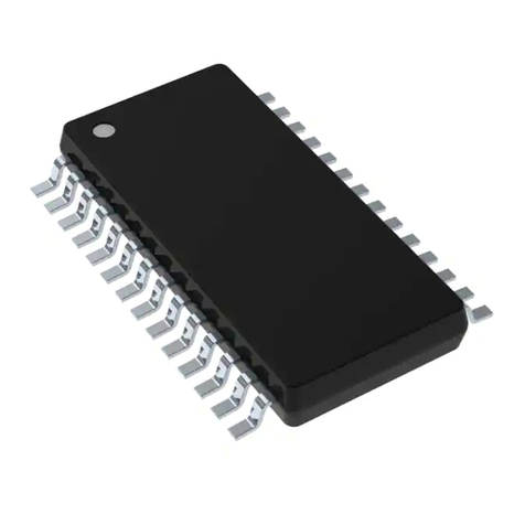
CS8952-CQ 0 to 70 °C 100-pin TQFP
CDB8952 Evaluation Board
TX_EN
TX_ER/TXD4
TXD[3:0]
TX_CLK
MDC
MII_IRQ
MDIO
CRS
COL
RX_ER/RXD4
RX_DV
RXD[3:0]
RX_CLK
RX_EN
TX+,
TX-
TX_NRZ+,
TX_NRZ-
RX_NRZ+,
RX_NRZ-
RX+,
RX-
LED1
LED2
LED3
LED4
LED5
10/100
M
U
X
4B/5B
Decoder Descrambler
Manchester
Encoder
Scrambler
Fiber NRZI
Interface
MLT-3
Encoder
10BaseT
Filter
Slew Rate
Control
M
U
X
10/100
4B/5B
Encoder
ECL Driver
ECL Receiver
Adaptive Eq. &
Baseline Wander
Compensation
10BaseT
Filter
LED
Drivers
100BaseT
Slicer
10BaseT
Slicer
Fiber NRZI
Interface
MLT-3
Decoder
Manchester
Decoder
Auto
Negotiation
Timing
Recovery
MII
Control/Status
Registers
Link
Management
CS8952 10BaseT/100Base-X
Transceiver
Media Independent Interface
(MII)
DS206PP3
OCT ‘01
CS8952
CrystalLAN™ 100BASE-X and 10BASE-T Transceiver

CS8952
2 CrystalLAN™ 100BASE-X and 10BASE-T Transceiver
TABLE OF CONTENTS
SPECIFICATIONS AND CHARACTERISTICS............................................................. 4
ABSOLUTE MAXIMUM RATINGS .......................................................................4
RECOMMENDED OPERATING CONDITIONS ...................................................4
QUARTZ CRYSTAL REQUIREMENTS ...............................................................4
DC CHARACTERISTICS .....................................................................................5
10BASE-T CHARACTERISTICS ......................................................................... 7
100BASE-X CHARACTERISTICS .......................................................................8
100BASE-TX MII RECEIVE TIMING - 4B/5B ALIGNED MODES ........................9
100BASE-TX MII RECEIVE TIMING - 5B BYPASS ALIGN MODE ...................10
100BASE-TX MII TRANSMIT TIMING - 4B/5B ALIGN MODES ........................11
100BASE-TX MII TRANSMIT TIMING - 5B BYPASS ALIGN MODE ................12
10BASE-T MII RECEIVE TIMING ......................................................................13
10BASE-T MII TRANSMIT TIMING ...................................................................14
10BASE-T SERIAL RECEIVE TIMING ..............................................................15
10BASE-T SERIAL TRANSMIT TIMING ............................................................16
AUTO NEGOTIATION / FAST LINK PULSE TIMING ........................................17
SERIAL MANAGEMENT INTERFACE TIMING .................................................18
INTRODUCTION .......................................................................................................... 19
High Performance Analog...................................................................................19
Low Power Consumption ....................................................................................19
Application Flexibility...........................................................................................19
Typical Connection Diagram ...............................................................................19
FUNCTIONAL DESCRIPTION ....................................................................................21
Major Operating Modes.......................................................................................21
100BASE-X MII Application (TX and FX) .....................................................21
Symbol Encoding and Decoding ...........................................................22
100 Mb/s Loopback ...............................................................................23
100BASE-X Repeater Application ...............................................................23
10BASE-T MII Application ...........................................................................24
Full and Half Duplex operation ..............................................................24
Collision Detection .................................................................................24
Jabber ...................................................................................................24
Link Pulses ............................................................................................24
Receiver Squelch ..................................................................................25
10BASE-T Loopback .............................................................................25
Carrier Detection ...................................................................................25
Contacting Cirrus Logic Support
For a complete listing of Direct Sales, Distributor, and Sales Representative contacts, visit the Cirrus Logic web site at:
http://www.cirrus.com/corporate/contacts/sales.cfm
Preliminary product information describes products which are in production, but for which full characterization data is not yet available. Advance product infor-
mation describes products which are in development and subject to development changes. Cirrus Logic, Inc. has made best efforts to ensure that the information
contained in this document is accurate and reliable. However, the information is subject to change without notice and is provided “AS IS” without warranty of
any kind (express or implied). Customers are advised to obtain the latest version of relevant information to verify, before placing orders, that information being
relied on is current and complete. All products are sold subject to the terms and conditions of sale supplied at the time of order acknowledgment, including those
pertaining to warranty, patent infringement, and limitation of liability. No responsibility is assumed by Cirrus Logic, Inc. for the use of this information, including
use of this information as the basis for manufacture or sale of any items, nor for infringements of patents or other rights of third parties. This document is the
property of Cirrus Logic, Inc. and by furnishing this information, Cirrus Logic, Inc. grants no license, express or implied under any patents, mask work rights,
copyrights, trademarks, trade secrets or other intellectual property rights of Cirrus Logic, Inc. Cirrus Logic, Inc., copyright owner of the information contained
herein, gives consent for copies to be made of the information only for use within your organization with respect to Cirrus Logic integrated circuits or other parts
of Cirrus Logic, Inc. The same consent is given for similar information contained on any Cirrus Logic website or disk. This consent does not extend to other
copying such as copying for general distribution, advertising or promotional purposes, or for creating any work for resale. The names of products of Cirrus Logic,
Inc. or other vendors and suppliers appearing in this document may be trademarks or service marks of their respective owners which may be registered in some
jurisdictions. A list of Cirrus Logic, Inc. trademarks and service marks can be found at http://www.cirrus.com
.

CS8952
CrystalLAN™ 100BASE-X and 10BASE-T Transceiver 3
10BASE-T Serial Application ....................................................................... 25
Auto-Negotiation ................................................................................................. 25
Reset Operation.................................................................................................. 26
LED Indicators..................................................................................................... 26
MEDIA INDEPENDENT INTERFACE (MII) ................................................................. 27
MII Frame Structure............................................................................................ 27
MII Receive Data................................................................................................. 28
MII Transmit Data................................................................................................ 28
MII Management Interface.................................................................................. 29
MII Management Frame Structure...................................................................... 29
CONFIGURATION ...................................................................................................... 30
Configuration At Power-up/Reset Time............................................................... 30
Configuration Via Control Pins............................................................................ 30
Configuration via the MII..................................................................................... 30
CS8952 REGISTERS .................................................................................................. 31
Basic Mode Control Register - Address 00h ..................................................... 32
Basic Mode Status Register - Address 01h ...................................................... 34
PHY Identifier, Part 1 - Address 02h ................................................................. 36
PHY Identifier, Part 2 - Address 03h ................................................................. 37
Auto-Negotiation Advertisement Register - Address 04h .................................. 38
Auto-Negotiation Link Partner Ability Register - Address 05h ........................... 39
Auto-Negotiation Expansion Register - Address 06h ........................................ 40
Auto-Negotiation Next-Page Transmit Register - Address 07h ......................... 41
Interrupt Mask Register - Address 10h ............................................................. 42
Interrupt Status Register - Address 11h ............................................................ 45
Disconnect Count Register - Address 12h ........................................................ 48
False Carrier Count Register - Address 13h ..................................................... 49
Scrambler Key Initialization Register - Address 14h ......................................... 50
Receive Error Count Register - Address 15h .................................................... 51
Descrambler Key Initialization Register - Address 16h ..................................... 52
PCS Sub-Layer Configuration Register - Address 17h ..................................... 53
Loopback, Bypass, and Receiver Error Mask Register - Address 18h ............. 56
Self Status Register - Address 19h ................................................................... 59
10BASE-T Status Register - Address 1Bh ........................................................ 61
10BASE-T Configuration Register - Address 1Ch ............................................ 62
DESIGN CONSIDERATIONS ...................................................................................... 64
Twisted Pair Interface ......................................................................................... 64
100BASE-FX Interface........................................................................................ 64
Internal Voltage Reference ................................................................................. 64
Clocking Schemes .............................................................................................. 65
Recommended Magnetics .................................................................................. 66
Power Supply and Decoupling............................................................................ 66
General Layout Recommendations..................................................................... 66
PIN DESCRIPTIONS ................................................................................................... 69
PACKAGE DIMENSIONS........................................................................................... 81

CS8952
4 CrystalLAN™ 100BASE-X and 10BASE-T Transceiver
1. SPECIFICATIONS AND CHARACTERISTICS
ABSOLUTE MAXIMUM RATINGS (AVSS, DVSS = 0 V, all voltages with respect to 0 V.)
WARNING: Operation at or beyond these limits may result in permanent damage to the device.
Normal operation is not guaranteed at these extremes.
RECOMMENDED OPERATING CONDITIONS (AVSS, DVSS = 0 V, all voltages with respect
to 0 V.)
QUARTZ CRYSTAL REQUIREMENTS (If a 25 MHz quartz crystal is used, it must meet the fol-
lowing specifications.)
Parameter Symbol Min Max Unit
Power Supply VDD
VDD_MII
-0.3
-0.3 6.0
6.0 V
Input Current Except Supply Pins - +/-10.0 mA
Input Voltage -0.3 VDD +0.3 V
Ambient Temperature Power Applied -55 +125 °C
Storage Temperature -65 +150 °C
Parameter Symbol Min Max Unit
Power Supply Core
MII VDD
VDD_MII
4.75
3.0 5.25
5.25 V
V
Operating Ambient Temperature TA070°C
Parameter Min Typ Max Unit
Parallel Resonant Frequency - 25.0 - MHz
Resonant Frequency Error (CL = 15 pF) -50 - +50 ppm
Resonant Frequency Change Over Operating Temperature -40 - +40 ppm
Crystal Load Capacitance - 15 - pF
Motional Crystal Capacitance - 0.021 - pF
Series Resistance - - 18 Ω
Shunt Capacitance - - 7 pF

CS8952
CrystalLAN™ 100BASE-X and 10BASE-T Transceiver 5
DC CHARACTERISTICS (Over recommended operating conditions)
Parameter Symbol Min Typ Max Unit
External Oscillator
XTAL_I Input Low Voltage VIXH -0.3 - 0.5 V
XTAL_I Input High Voltage VIXH 3.5 - VDD+0.5 V
XTAL_I Input Low Current IIXL -40 - - µA
XTAL_I Input High Current IIXH --40µA
XTAL_I Input Capacitance CL-35pF
XTAL_I Input Cycle Time tIXC 39.996 - 40.004 ns
XTAL_I Input Low Time tIXL 18 - 22 ns
XTAL_I Input High Time tXH 18 - 22 ns
Power Supply
Power Supply Current 100BASE-TX (Note 1)
100BASE-FX (Note 1)
10BASE-T (Note 1)
IDD -
-
-
135
90
80
145
-
-
mA
Hardware Power-Down (Note 1)I
DDHPDN -900-µA
Software Power-Down (Note 1)I
DDSPDN -20-mA
Low Power Power-Up (Note 1)I
DDSLPUP -900-µA
Digital I/O
Output Low Voltage
CLK25, MII_IRQ, SPD10, SPD100 IOL =4.0mA
LED[4:0] IOL =10.0mA
VOL -
-
-
-
0.4
0.4
V
Output Low Voltage (MII_DRV = 1)
COL, CRS, MDIO, RXD[3:0],
RX_CLK, RX_DV, RX_ER,
TX_CLK IOL =4.0mA
VDD_MII = 5V; IOL =43.0mA
VDD_MII = 3.3V, IOL =26.0mA
VOL
-
-
-
-
-
-
0.4
3.05
2.1
V
Output Low Voltage (MII_DRV = 0)
COL, CRS, MDIO, RXD[3:0],
RX_CLK, RX_DV, RX_ER,
TX_CLK IOL =4.0mA
VOL
--0.4
V
Output High Voltage
CLK25, SPD10, SPD100 IOH =-4.0mA VOH 2.4 - - V
Output High Voltage (MII_DRV = 1)
COL, CRS, MDIO, RXD[3:0],
RX_CLK, RX_DV, RX_ER,
TX_CLK IOH=-4.0mA
VDD_MII=5V;I
OH =-20.0mA
VDD_MII=3.3V,I
OH =-20.0mA
VOH
2.4
1.1
1.1
-
-
-
-
-
-
V

CS8952
6 CrystalLAN™ 100BASE-X and 10BASE-T Transceiver
Notes: 1. With digital outputs connected to CMOS loads.
Output High Voltage (MII_DRV = 0)
COL, CRS, MDIO, RXD[3:0],
RX_CLK, RX_DV, RX_ER,
TX_CLK IOH =-4.0mA
VOH
2.4 - -
V
Input Low Voltage
All Inputs Except AN[1:0], TCM, TXSLEW[1:0] VIL --0.8V
Input High Voltage
All Inputs Except AN[1:0], TCM, TXSLEW[1:0] VIH 2.0 - - V
Tri-Level Input Voltages
AN[1:0], TCM, TXSLEW[1:0] VIL
VIM
VIH
-
1/3 VDD_MII
+20%
2/3 VDD_MII
+20%
-
-
-
1/3 VDD_MII
-20%
2/3 VDD_MII
-20%
-
V
Input Low Current
MDC, TXD[3:0], TX_CLK, TX_EN,
TX_ER VI=0.0V
MDIO VI=0.0V
IIL
-20
-3800
-
-
-
-
µA
Input High Current
MDC, TXD[3:0], TX_CLK, TX_EN,
TX_ER VI=5.0V
MDIO VI=5.0V
IIH
-
-
-
-
200
20
µA
Input Leakage Current
All Other Inputs 0<=V<=VDD
ILEAK -10 - +10 µA
DC CHARACTERISTICS (CONTINUED) (Over recommended operating conditions)
Parameter Symbol Min Typ Max Unit

CS8952
CrystalLAN™ 100BASE-X and 10BASE-T Transceiver 7
10BASE-T CHARACTERISTICS
Parameter Symbol Min Typ Max Unit
10BASE-T Interface
Transmitter Differential Output Voltage (Peak) VOD 2.2 - 2.8 V
Receiver Normal Squelch Level (Peak) VISQ 300 - 525 mV
Receiver Low Squelch Level (LoRxSquelch bit
set) VSQL 125 - 290 mV
10BASE-T Transmitter
TXD Pair Jitter into 100 ΩLoad tTTX1 --8ns
TXD Pair Return to ≤50 mV after Last Positive
Transition tTTX2 --4.5µs
TXD Pair Positive Hold Time at End of Packet tTTX3 250 - - ns
10BASE-T Receiver
Allowable Received Jitter at Bit Cell Center tTRX1 - - +/-13.5 ns
Allowable Received Jitter at Bit Cell Boundary tTRX2 - - +/-13.5 ns
10BASE-T Link Integrity
First Transmitted Link Pulse after Last Transmit-
ted Packet tLN1 15 16 17 ms
Time Between Transmitted Link Pulses tLN2 15 16 17 ms
Width of Transmitted Link Pulses tLN3 60 - 200 ns
Minimum Received Link Pulses Separation tLN4 257ms
Maximum Received Link Pulse Separation tLN5 25 52 150 ms
Last Receive Activity to Link Fail (Link Loss
Timer) tLN6 50 52 150 ms
10Base-T Jabber/Unjabber Timing
Maximum Transmit Time - 105 - ms
Unjabber Time - 406 - ms
TXD±
RXD±
LINKLED
t
LN1
t
LN3
t
LN2
t
LN5
t
LN4
t
LN6
RXD±
t
RTX1
t
RTX2
t
RTX3
t
RTX4
Carrier Sense
(Internal)
TXD±
t
TTX1
t
TTX3
t
TTX2

CS8952
8 CrystalLAN™ 100BASE-X and 10BASE-T Transceiver
100BASE-X CHARACTERISTICS
Parameter Symbol Min Typ Max Unit
100BASE-TX Transmitter
TX Differential Output Voltage (Peak) VOP 0.95 - 1.05 V
Signal Amplitude Symmetry VSYM 98 - 102 %
Signal Rise/Fall Time tRF 3.0 - 5.0 ns
Rise/Fall Symmetry tRFS --0.5ns
Duty Cycle Distortion tDCD --+/-0.5ns
Overshoot/Undershoot tOS --5%
Transmit Jitter tJT - 400 1400 ps
TX Differential Output Impedance ZOUT -100-ohms
100BASE-TX Receiver
Receive Signal Detect Assert Threshold - - 1.0 Vp-p
Receive Signal Detect De-assert Threshold 0.2 - - Vp-p
Receive Signal Detect Assert Time - - 1000 µs
Receive Signal Detect De-assert Time - - 350 µs
100BASE-FX Transmitter
TX_NRZ+/- Output Voltage - Low V1-1.830 - -1.605 V
TX_NRZ+/- Output Voltage - High V2-1.035 - -0.880 V
Signal Rise/Fall Time TRF --1.6ns
100Base-FX Receiver
RX_NRZ+/- Input Voltage - Low V3-1.830 - -1.605 V
RX_NRZ+/- Input Voltage - High V4-1.035 - -0.880 V
Common Mode Input Range VCMIP -3.56-V
V1V2
VDD
0
TX_NRZ+/- V3V4
RX_NRZ+/-
RX/TX Signaling for 100Base-FX

CS8952
CrystalLAN™ 100BASE-X and 10BASE-T Transceiver 9
100BASE-TX MII RECEIVE TIMING - 4B/5B ALIGNED MODES
Parameter Symbol Min Typ Max Unit
RX_CLK Period tP-40-ns
RX_CLK Pulse Width tWL, tWH -20-ns
RXD[3:0],RX_ER/RXD4,RX_DV setup to rising
edge of RX_CLK tSU 10 - - ns
RXD[3:0],RX_ER/RXD4,RX_DV hold from rising
edge of RX_CLK tHD 10 - - ns
CRStoRXDlatency 4BAligned
5B Aligned tDLAT 2
23-6
3-6 8
8BT
“Start of Stream”to CRS asserted tCRS1 -1011BT
“End of Stream”to CRS de-asserted tCRS2 --21BT
“Start of Stream”to COL asserted tCOL1 --11BT
“End of Stream”to COL de-asserted tCOL2 --21BT
RX_EN asserted to RX_DV, RXD[3:0] valid tEN -TBD-ns
RX_EN de-asserted to RX_DV, RXD[3:0].
RX_ER/RXD4 in high impedance state tDIS -TBD-ns
RX_CLK
RXD[3:0],
CRS
tCRS1
tCOL2
tRLAT
Start of
Stream End of
Stream
RX_EN
RX+/-
RX_DV
IN
OUT
IN
OUT
OUT
OUT
OUT
COL
tCOL1
tCRS2
tHD
tEN
tDIS
RX_ER/RXD4
tWL tWH
tP
tSU

CS8952
10 CrystalLAN™ 100BASE-X and 10BASE-T Transceiver
100BASE-TX MII RECEIVE TIMING - 5B BYPASS ALIGN MODE
Parameter Symbol Min Typ Max Unit
RX_CLK Period tP-40-ns
RX_CLK Pulse Width tWL, tWH -20-ns
RXD[4:0]setuptorisingedgeofRX_CLK t
SU 10 - - ns
RXD[4:0] hold after rising edge of RX_CLK tHD 10 - - ns
Start of 5B symbol to symbol output on RX[4:0]
5B Mode tRLAT 5-9BT
RX_CLK
RXD[4:0],
tRLAT
RX Symbol
0RX Symbol
N
RX+/- IN
OUT
OUT
tHD
tWL tWH
tP
tSU
RX Symbol
N-1
RX Data
0RX Data
1

CS8952
CrystalLAN™ 100BASE-X and 10BASE-T Transceiver 11
100BASE-TX MII TRANSMIT TIMING - 4B/5B ALIGN MODES
Parameter Symbol Min Typ Max Unit
TXD[3:0] Setup to TX_CLK High tSU1 10 - - ns
TX_EN Setup to TX_CLK High tSU2 10 - - ns
TXD[3:0] Hold after TX_CLK High tHD1 0--ns
TX_ER Hold after TX_CLK High tHD2 0--ns
TX_EN Hold after TX_CLK High tHD3 0--ns
TX_EN “high”to CRS asserted latency tCRS1 -8BT
TX_EN “low”to CRS de-asserted latency tCRS2 -8BT
TX_EN “high”to TX+/- output (TX Latency) tLAT 678BT
TX_CLK
TX_EN
TXD[3:0],
CRS
TX+/-
tSU2
tSU1
tHD2
tHD1
tCRS1 tCRS2
tLAT
Input/Output
Input
Input
Output
Output
TX_ER/TXD4 Data
IN
Symbol
Out

CS8952
12 CrystalLAN™ 100BASE-X and 10BASE-T Transceiver
100BASE-TX MII TRANSMIT TIMING - 5B BYPASS ALIGN MODE
Parameter Symbol Min Typ Max Unit
TXD[4:0] Setup to TX_CLK High tSU1 10 - - ns
TXD[4:0] Hold after TX_CLK High tHD1 0--ns
TX_ER Hold after TX_CLK High tHD2 0--ns
TXD[4:0] Sampled to TX+/- output (TX Latency) tLAT -67ns
TX_CLK
TXD[4:0]
TX+/-
tSU1 tHD1
tLAT
Symbol
OUT
Input/Output
Input
Output
Data
IN

CS8952
CrystalLAN™ 100BASE-X and 10BASE-T Transceiver 13
10BASE-T MII RECEIVE TIMING
Parameter Symbol Min Typ Max Unit
RX_CLK Period tP-400-ns
RX_CLK Pulse Width tWL, tWH -200-ns
RXD[3:0],RX_ER,RX_DVsetuptorisingedgeof
RX_CLK tSU 30 - - ns
RXD[3:0], RX_ER, RX_DV hold from rising edge
of RX_CLK tHD 30 - - ns
RX data valid from CRS tRLAT -810BT
RX+/- preamble to CRS asserted tCRS1 -57BT
RX+/- end of packet to CRS de-asserted tCRS2 2.5 3 BT
RX+/- preamble to COL asserted tCOL1 0-7BT
RX+/- end of packet to COL de-asserted tCOL2 --3BT
RX_EN asserted to RX_DV, RXD[3:0], RX_ER
valid tEN - - 60 ns
RX_EN de-asserted to RX_DV, RXD[3:0]. RX_ER
in high impedance state tDIS - - 60 ns
RX_CLK
RXD[3:0],
CRS
tCRS1
tCOL2
tRLAT
RX_EN
RX+/-
RX_DV
IN
OUT
IN
OUT
OUT
OUT
COL
tCOL1
tCRS2
tHD
tEN
tDIS
RX_ER
tWL tWH
tP
tSU
OUT

CS8952
14 CrystalLAN™ 100BASE-X and 10BASE-T Transceiver
10BASE-T MII TRANSMIT TIMING
Parameter Symbol Min Typ Max Unit
TXD[3:0] Setup to TX_CLK High tSU1 10 - - ns
TX_ER Setup to TX_CLK High tSU2 10 - - ns
TX_EN Setup to TX_CLK High tSU3 10 - - ns
TXD[3:0] Hold after TX_CLK High tHD1 0--ns
TX_ER Hold after TX_CLK High tHD2 0--ns
TX_EN Hold after TX_CLK High tHD3 0--ns
TX_EN “high”to CRS asserted latency tCRS1 0-4BT
TX_EN “low”to CRS de-asserted latency tCRS2 0-16BT
TX_EN “high”to TX+/- output (TX Latency) tLAT 6-14BT
SQE Timing
COL (SQE) Delay after CRS de-asserted tCOL 0.65 0.9 1.6 µs
COL (SQE) Pulse Duration tCOLP 0.65 1.0 1.6 µs
TX_CLK
TX_EN
TX_ER
TXD[3:0]
CRS
TX+/-
tSU3
tSU2
tSU1
tHD3
tHD2
tHD1
tCRS1 tCRS2
tLAT
Valid
Data
Input/Output
Input
Input
Input
Output
Output
TX_CLK
tSQE
COL tSQEP
Input/Output
Output
SQE Timing
10BASE-T Transmit Timing

CS8952
CrystalLAN™ 100BASE-X and 10BASE-T Transceiver 15
10BASE-T SERIAL RECEIVE TIMING
Parameter Symbol Min Typ Max Unit
RX+/- active to RXD[0] active tDATA - - 1200 ns
RX+/- active to CRS active tCRS --600ns
RXD[0] setup from RX_CLK tRDS 35 - - ns
RXD[0] hold from RX_CLK tRDH 50 - - ns
RX_CLK hold after CRS off tRCH 5--ns
RXD[0] throughput delay tRD --250ns
CRS turn off delay tCRSOFF --400ns
RX_CLK
RXD[0]
CRS
tCRS
RX+/- IN
OUT
OUT
tCRSOFF
tHD
tSU
OUT
tDATA
tRD
tRCH

CS8952
16 CrystalLAN™ 100BASE-X and 10BASE-T Transceiver
10BASE-T SERIAL TRANSMIT TIMING
Parameter Symbol Min Typ Max Unit
TX_EN Setup from TX_CLK tEHCH 10 - - ns
TX_EN Hold after TX_CLK tCHEL 10 - - ns
TXD[0] Setup from TX_CLK tDSCH 10 - - ns
TXD[0] Hold after TX_CLK tCHDU 10 - - ns
Transmit start-up delay tSTUD --500ns
Transmit throughput delay tTPD --500ns
TX_CLK
TX_EN
TXD[3:0]
TX+/-
tEHCH
tDSCH
tCHEL
tCHDU
tSTUD
Valid
Data
Input/Output
Input
Input
Output
tPD

CS8952
CrystalLAN™ 100BASE-X and 10BASE-T Transceiver 17
AUTO NEGOTIATION / FAST LINK PULSE TIMING
Parameter Symbol Min Typ Max Unit
FLP burst to FLP burst tBTB 15 16 17 ms
FLP burst width tFLPW -2-ms
Clock/Data pulses per burst -17 - 33 ea.
Clock/Data pulse width tPW -100-ns
Clock pulse to Data pulse tCTD 55.5 64 69.5 µs
Clock pulse to clock pulse tCTC 111 128 139 µs
tFLPW
tBTB
Clock
Pulse Data
Pulse Clock
Pulse
tPW
tCTD
tCTC
tPW
TX+/-
TX+/-

CS8952
18 CrystalLAN™ 100BASE-X and 10BASE-T Transceiver
SERIAL MANAGEMENT INTERFACE TIMING
Parameter Symbol Min Typ Max Unit
MDC Period tp60 - - ns
MDC Pulse Width tWL,tWH 40 - 60 %
MDIO Setup to MDC (MDIO as input) tMD1 10 - - ns
MDIO Hold after MDC (MDIO as input) tMD2 10 - - ns
MDC to MDIO valid (MDIO as output) tMD3 0 - 40 ns
MDC
MDIO
MDIO
Valid Data
DIRECTION:
IN or OUT of chip
IN
IN
OUT
t
MD1
t
MD2
t
MD3
Valid Data
Valid Data

CS8952
CrystalLAN™ 100BASE-X and 10BASE-T Transceiver 19
2. INTRODUCTION
The CS8952 is a complete physical-layer transceiv-
er for 100BASE-TX and 10BASE-T applications.
Additionally, the CS8952 can be used with an ex-
ternal optical module for 100BASE-FX.
2.1 High Performance Analog
The highly integrated mixed-signal design of the
CS8952 eliminates the need for external analog cir-
cuitry such as external transmit or receive filters.
The CS8952 builds uponCirrus Logic’s experience
in pioneering the high-volume manufacturing of
10BASE-T integrated circuits with “true” internal
filters. The CS8952, CS8920, CS8904, and
CS8900 include fifth-order, continuous-time But-
terworth 10BASE-T transmit and receive filters, al-
lowing those products to meet 10BASE-T wave
shape, emission, and frequency content require-
ments without external filters.
2.2 Low Power Consumption
The CS8952 is implemented in low power CMOS,
consuming only 135 mA typically. Three low-pow-
er modes are provided to make the CS8952 ideal
for power sensitive applications such as CardBus.
2.3 Application Flexibility
The CS8952’s digital interface and operating
modes can be tailored to efficiently support a wide
variety of applications. For example, the Media In-
dependent Interface (MII) supports 100BASE-TX,
100BASE-FX and 10BASE-T NIC cards, switch
ports and router ports. Additionally, the low-laten-
cy “repeater” interface mode minimizes data delay
through the CS8952, facilitating system compli-
ance with overall network delay budgets. To sup-
port 10BASE-T applications, the CS8952 provides
a 10BASE-T serial port (Seven-wire ENDEC inter-
face).
2.4 Typical Connection Diagram
Figure 1 illustrates a typical MII to CS8952 appli-
cation with twisted-pair and fiber interfaces. Refer
to the Analog Design Considerations section for
detailed information on power supply requirements
and decoupling, crystal and magnetics require-
ments, and twisted-pair and fiber transceiver con-
nections.
3. FUNCTIONAL DESCRIPTION
The CS8952 is a complete physical-layer transceiv-
er for 100BASE-TX and 10BASE-T applications.
It provides a Physical Coding Sub-layer for com-
munication with an external MAC (Media Access
Controller). The CS8952 also includes a complete
Physical Medium Attachment layer and a
100BASE-TX and 10BASE-T Physical Medium
Dependent layer. Additionally, the CS8952 pro-
vides a PECL interface to an external optical mod-
ule for 100BASE-FX applications.
The primary digital interface to the CS8952 is an
enhanced IEEE 802.3 Media Independent Interface
(MII). The MII supports parallel data transfer, ac-
cess to the CS8952 Control and Status registers,
and several status and control pins. The CS8952's
operating modes can be tailored to support a wide
variety of applications, including low-latency
100BASE-TX repeaters, switches and MII-based
network interface cards.
For 100BASE-TX applications, the digital data in-
terface can be either 4-bit parallel (nibbles) or 5-bit
parallel (code-groups). For 10BASE-T applica-
tions, the digital data format can be either 4-bit par-
allel (nibbles) or one-bit serial.
The CS8952 is controlled primarily by configura-
tion registers via the MII Management Interface.
Additionally, a number of the most fundamental
register bits can be set at power-up and reset time
by connecting pull-up or pull-down resistors to ex-
ternal pins.
The CS8952's MII interface is enhanced beyond
IEEE requirements by register extensions and the
addition of pins for MII_IRQ,RX_EN,andISO-
DEF signals. The MII_IRQ pin provides an inter-

CS8952
20 CrystalLAN™ 100BASE-X and 10BASE-T Transceiver
VSS18 RES VSS17
4.99 k
Ω
25 MHz
XTAL_I XTAL_O
33
Ω
MDIO
33
Ω
33
Ω
33
Ω
33
Ω
33
Ω
33
Ω
MDC
TXD
TX_ER/TXD[4]
TX_EN
TX_CLK
RX_CLK
RXD[3]/PHYAD[3]
RX_ER/RXD[4]/PHYAD[4]
RX_DV/MII_DRV
COL/PHYAD0
CRS/PHYAD[2]
4
MII
I/F
SPEED10
SPEED100
680
Ω
680
Ω
680
Ω
680
Ω
680
Ω
680
Ω
680
Ω
LED1
LED2
LED3
LED4
LED5
VDD
VDD_MII
VDD_MII
+5 V
10 µF 0.1 µF
10 µF 0.1 µF
11
RSVD VSS TEST0 TEST1
721
0.1 µF 0.1 µF
51
Ω
51
Ω
8
7
51
Ω
6
5
51
Ω
4
3
2
1
51
Ω
51
Ω
75
Ω
75
Ω
0.01 µF
2KV
SHLD
SHLD
RJ45
RX+
RX-
TX+
TX-
130
Ω
191
Ω
82
Ω
68
Ω
0.1 µF
63.4
Ω
82
Ω
82
Ω
+5 V
+5 V
0.1 µF 0.1 µF
49.9
Ω
49.9
Ω
130
Ω
130
Ω
SD+
TD-
TD+
VCC
VCC
RD-
RD+
VEE
VEE
FIBER
TRANSCEIVER
SIGNAL+
SIGNAL-
TX_NRZ-
TX_NRZ+
RX_NRZ-
RX_NRZ+
AN0
AN1
NC
NC
CS8952
RX_EN
PWRDN
REPEATER
BPSCR
BP4B5B
BPALIGN
LPBK
ISODEF
10BT_SER
RESET
MII_IRQ
CONTROL
I/F
LPSTRT
TCM
TXSLEW0
TXSLEW1
NC
NC
1.5 k
Ω
VDD_MII 0.1 µF
49.9
Ω
49.9
Ω
+5 V
0.1 µF
0.1 µF
33
Ω
RXD[2]
33
Ω
RXD[1]/PHYAD[1]
33
Ω
RXD[0]
VDD_MII
4.7 k
3
4.7 k
Ω
4.7 k
Ω
Figure 1. Typical Connection Diagram
This manual suits for next models
1
Table of contents
Other Cirrus Logic Transceiver manuals
