CJB WMX-E38450 User manual

WMX-E38450 Intel BayTrail E3845
User Manual Rev. 02, Jul. 2014

2
Contents
Chapter 1 Product Information ................................................................................ 4
1.1 Block Diagram ............................................................................................. 4
1.2 Features ....................................................................................................... 5
1.3 PCB Layout ................................................................................................. .8
1.4 Jumper Setting .......................................................................................... 10
1.5 Connector Function List .......................................................................... .13
1.6 Connector Definitions .............................................................................. .15
1.6 I/O Ports Power Output (max.) ………………………………………………..32
Chapter 2 BIOS Setup ............................................................................................ 34
2.1 Main Menu .................................................................................................. 34
2.2 Advanced Menu ......................................................................................... 35
2.3 ACPI Settings ............................................................................................. 37
2.4 Super IO Configuration ............................................................................. 38
2.5 Serial Port 1 Configuration ...................................................................... .39
2.6 Serial Port 2 Configuration ....................................................................... 40
2.7 Serial Port 3 Configuration ...................................................................... .41
2.8 Serial Port 4 Configuration ...................................................................... .42
2.9 Serial Port 5 Configuration ...................................................................... .43
2.10 Serial Port 6 Configuration .................................................................... .44
2.11 PC Health Status ..................................................................................... .45
2.12 Smart Fan Mode Configuration ............................................................. .46
2.13 CPU Configuratio .................................................................................... .47
2.14 IDE Configuration ................................................................................... .48
2.15 Network Stack Configuration ................................................................ .50
2.16 Compatibility Support Module Configuration ...................................... .51
2.17 USB Configuration ................................................................................. .53
2.18 Chipset .................................................................................................... .55
2.19 Memory Information ............................................................................... .56
2.20 Intel IGD Configuration .......................................................................... .57
2.21 USB Configuration .................................................................................. 60
2.22 XHCI Mode ............................................................................................... 61
2.23 PCI Express Configuration .................................................................... .62
2.24 Passeord Configuration.……………………………………………………...63
2.25 Boot Configuration ................................................................................. .64
2.25 Save Changes and Exit………………………………………………………..65
Chapter 3 Drivers Installation ................................................................................ 68

3
3.1 Intel Chipset Device Software .................................................................. 68
3.2 Intel Graphic Media Accelerator Driver .................................................... 70
3.3 LAN Driver .................................................................................................. 74
3.4 Audio Driver. .............................................................................................. 77
3.5 TXE Driver………………………………………………………………………...77
3.6 USB Driver ……………………………………………………………………….80
Appendix A: Watchdog Timer ................................................................................ 82
Appendix B: GPIO .................................................................................................. 85
4
Chapter 1 Product Information
This chapter introduces the product features, jumper and connector information.
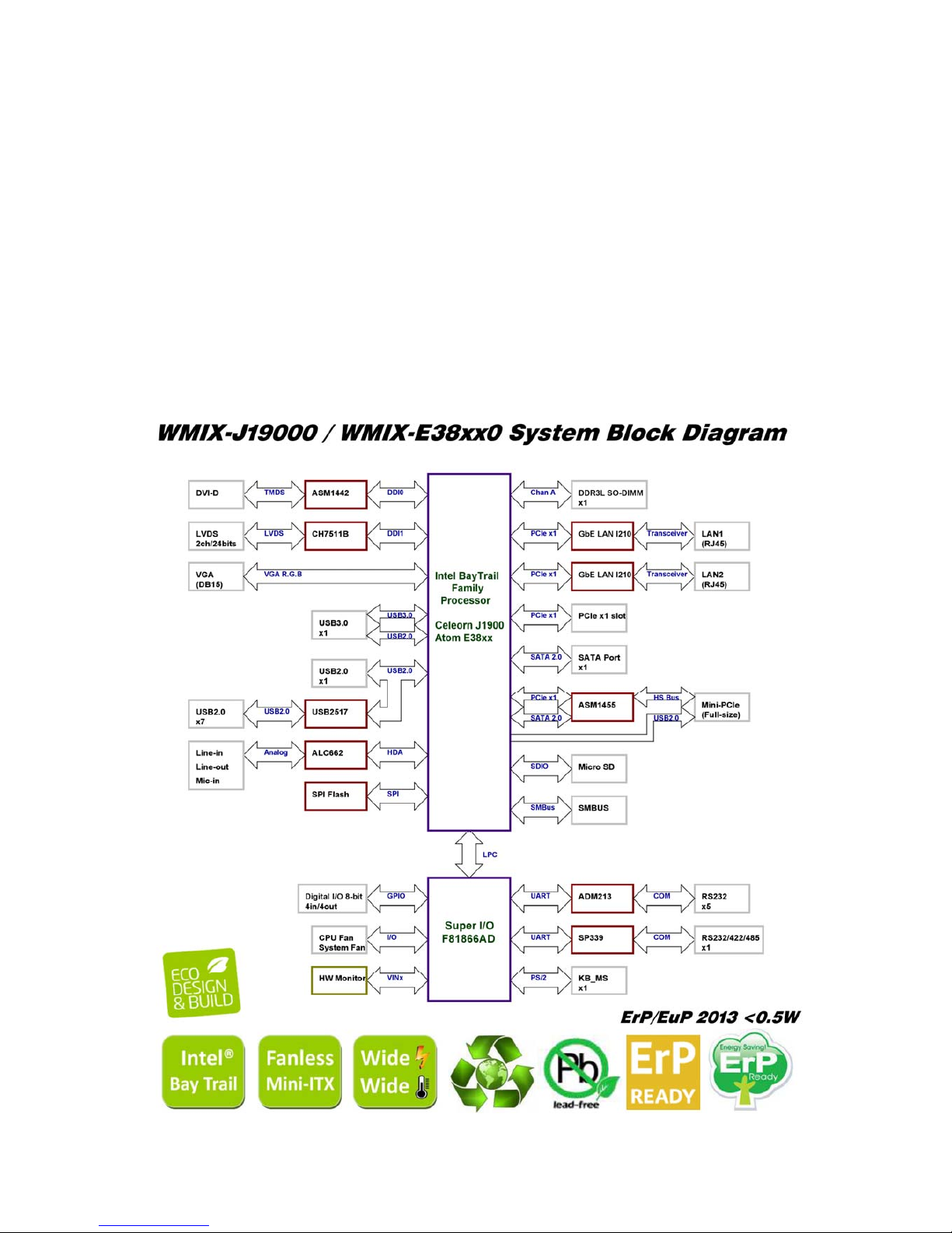
1.1 Block Diagram
The block diagram below shows the architecture and main components of the
WMX-E38450. The key component on the board is the Intel® Atom™ E3845
(Bay Trail) platform controller SoC.
5
1.2 Features
System Processor/
Chipsets
Processor
Intel®Atom™ Processor E3845 Product
(Bay Trail Platform)
FCBGA1170 Package 25.0mm x 27.0mm
BIOS AMI®BIOS, 64Mbit SPI Low Power Flash ROM
Memory
Technology
Atom™ Processors DDR3L 1333 MT/s
DDR3L DRAM Device Technology
—Standard 1Gb/2Gb/4Gb technologies and addressing.
—Read latency 5, 6, 7, 8, 9, 10, 11.
—Write latency 5, 6, 7, 8.
Max. Capacity Up to 8GB DDR3L DRAM
Socket 1 x DDR3L SO-DIMM (+1.35V)
Display
Chipset Intel®7th generation (Gen 7) graphics and media
encode/decode engine
VRAM Shared system memory up to 512MB (max.)
LVDS 24bit, Dual Channel
max resolution up to 1920 x 1200 @ 60Hz
VGA Analog Display:
max resolution up to 2560 x 1600 @ 60Hz
DVI-D Digital Display:
max resolution up to 1920 x 1200 @ 60Hz
Any 2
Displays
(1) LVDS+DVI-D
(2) LVDS+VGA
(3) DVI-D+VGA
Ethernet
Interface PCIe x1 Gigabit LAN 10/100/1000 Mb/s
Controller LAN1: Intel®Ethernet Controller I210
LAN2: Intel®Ethernet Controller I210
Audio
Interface Intel®High Definition Audio
Controller Realtek®ALC662-VD0 HD Audio Codec
6
Expansion Slot
PCIe x1 1
MINI-PCIE 1 (Full size with mSATA support by jumper
selector and SIM Card Board)
SATA
Max. Data
Transfer Rate SATA II:3.0Gb/s
Port
SATA II x1,
mSATA x1 (Share MINI-PCIE slot)
Integrated AHCI controller
Onboard Conn.
and Pin-Header
ATX 12V 1 (2x2 pin)
COM 4 (RS-232)
CPU Fan 1 (4pin.)
DIO 4 in/4 out (sink 6A x2)
FP_HDA 1 (Line-in2/Mic-in2)
FRONT 1 (Power/HDD/Suspend-LED/PwrBTN/RstBTN)
LVDS 1 (with Inverter power pin header)
Micro SD 1 (MicroSD/T-Flash, support SDHC)
PS/2 1 (PS/2 Keyboard and Mouse)
SATA II 1
SMBus 1
SYS Fan 1 (3pin.)
USB 2.0 2 (x4 ports)
WEBCAM 1 (USB 2.0 Interface)
Rear I/O
Audio 3 (Line-in, Line-out, Mic-in)
COM
2 (1xRS232,1xRS232/RS422/RS485); all support
12V/5V/RI# jumper selector.
※1. COM2 RS-422/485 support Half/Full Duplex.
※2. COM2 RS-232 Slew Rate 1Mbps (max.).
※3. COM2 RS-422/485 Slew Rate 20Mbps (max.).
DC-Jack 1 (+12Vdc ~ +24Vdc)
7
Rear I/O
DVI-D 1
LAN 2 x RJ45
USB 2.0 3
USB 3.0 1
VGA 1
Power
DC-Jack 1 (+12Vdc ~ +24Vdc)
ATX 4P 1 (only +12Vdc)
Watchdog Timer
Interval Programmable 1~255 sec./min.
Output System reset
Energy EuP/ErP EuP/ErP 2013 Ready
Power off mode (G3) < 0.5W
Environment
Operating
Temp.
0°C ~ +60°C (standard)
-20°C~ 70°C (optional)
-40°C~ 70°C (optional)
Storage
Temp.
-40°C ~ +80°C and 60°C @ 95% RH
non-condensing
Relative
Humidity 0%~ 95% (non-condensing)
Form Factor Dimension
(L*W)
Mini-ITX
170mm x 170mm (6.69” x 6.69”)
*** WMX-E38450 base unit will be RoHS / Halogen free compliant from LP/MP phase.
*** The content is subjected to change without notice.
Intel®
BayTrail
DVI‐D/VGA
/LVDS24bitFanless
Mini‐ITX
Wide
Wide
DualIntel®
GbELAN
USB2.0x7
USB3.0x1
RS‐232x5
x1
RS‐422
RS‐485
SATAx1
mSATAx1
MicroSDx1
DualDisplay
ErP/EuP
READY
DIOx8
Watchdog
8
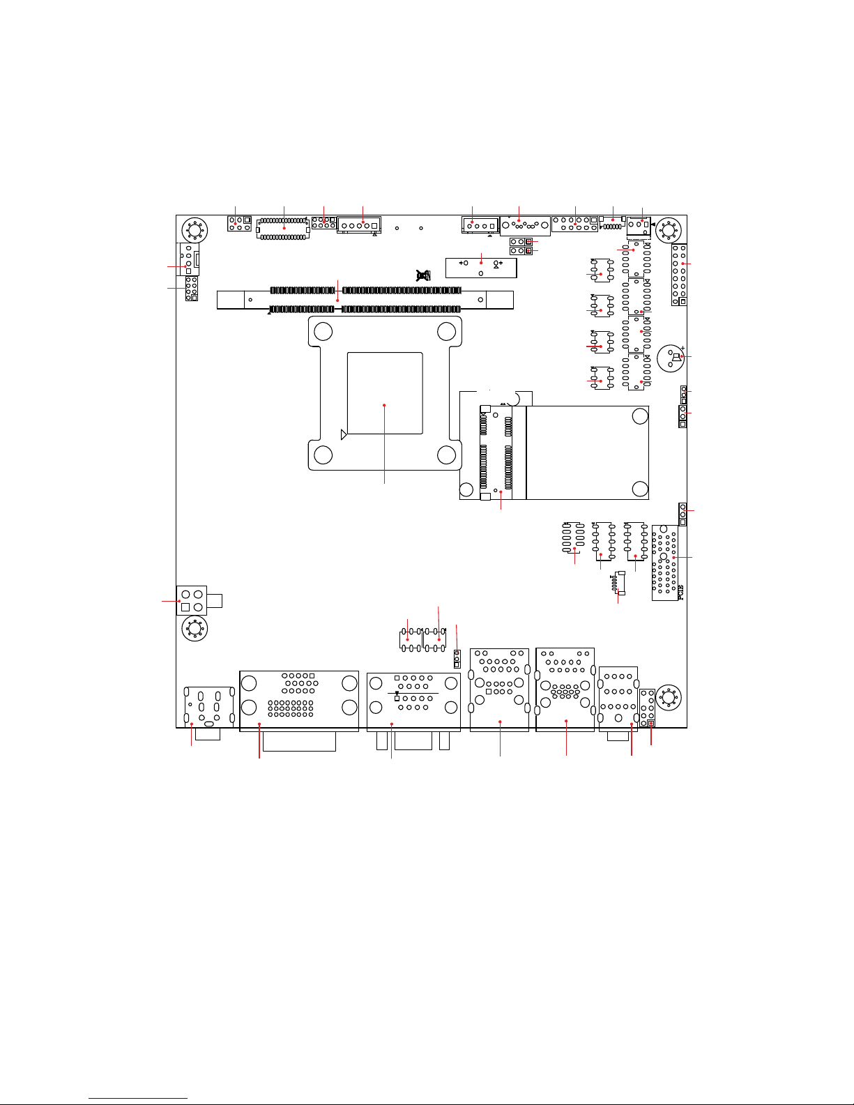
1.3 PCB Layout
WMX‐E38450To pView
CPUFAN
SPI
JPLVDS LVDS JLVDS INV SATAPWR SATA
JTRTC
JCMOS
DIO KB_MS SYSFAN
JPCOM3
JPCOM4
JPCOM5
JPCOM6
FRONT
BZ
COM3
COM4
JMINI-PCIE
JPWR
COM5
COM6
BAT1
CHA-DIMM
CPU
PWR2
PWR1
DVI-D_VGA COM1_COM2
JPCOM2
JPCOM1
JCOM2
USB2_LAN2 USB1_LAN1 AUDIO
FP_HDA
PCIE
SMB
WEBCAM
LPC USB3 USB4
SIMBD
MINI-PCIE
9
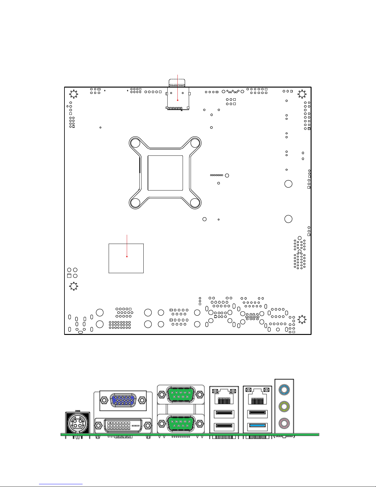
WMX‐E38450B ottomView
MICRO-SD
BARCODR LABEL
WMX‐E38450Rea rI/OView
PWR1DVI‐D_VGACOM1_COM2USB2_LAN2USB1_LAN1AUDIO

10
1
2
3
1
2
3
1
2
3
1
2
3
1
2
3
1
2
3
1
2
3
1
2
3
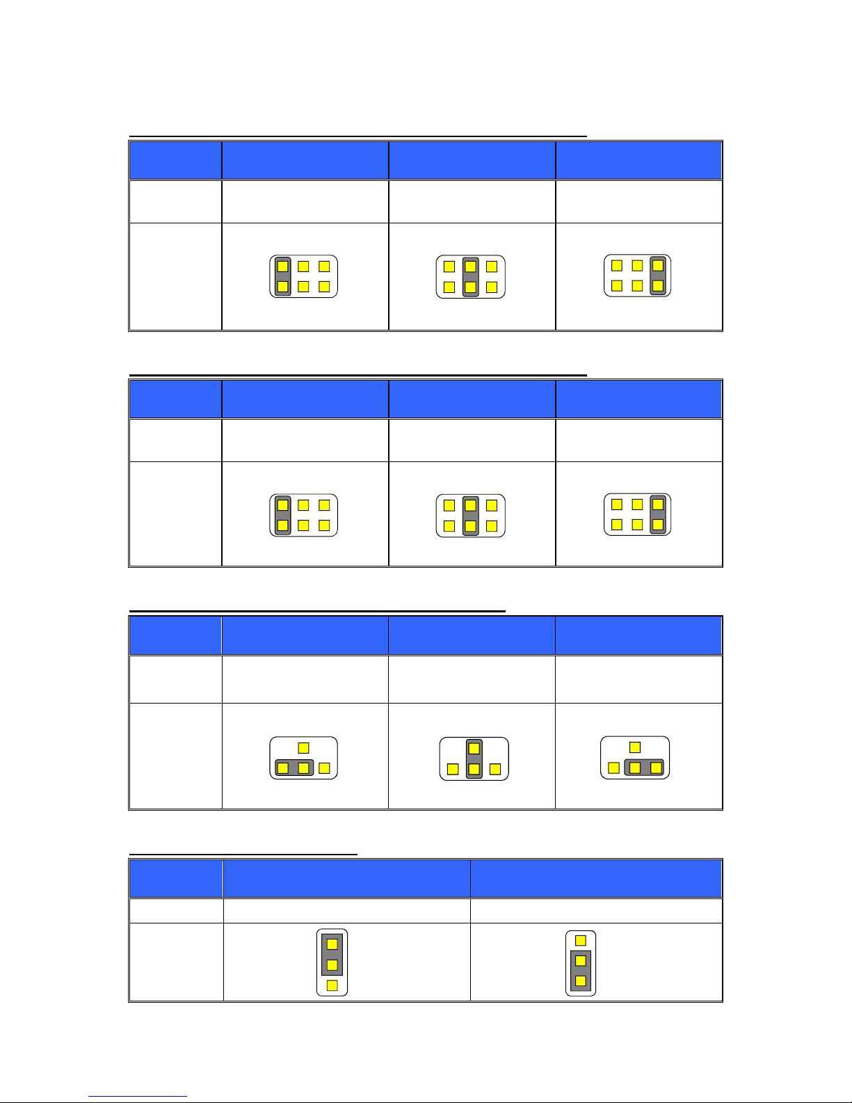
1.4 Jumper Setting
JCMOS: CMOS Clear Selection
Pin No. 1-2 2-3
Function Normal Operation (Default) Clear CMOS Contents
Jumper
Setting
JTRTC: RTC Register Clear Selection
Pin No. 1-2 2-3
Function Normal Operation (Default) Clear RTC Register Contents
Jumper
Setting
JCOM2: COM2 RS-232/422/485 Slew Rate Selection
Pin No. 1-2 2-3
Function RS-232 Slew Rate 250Kbps
RS-422/RS-485 Slew Rate 250Kbps
(Default)
RS-232 Slew Rate 1Mbps
RS-422/RS-485 Slew Rate 20Mbps
Jumper
Setting
JMINI-PCIE: Mini-PCIe / mSATA Function (by manual setting)
Pin No. 1-2 2-3
Function MINI-PCIE = PCIe signal
Mini-PCIe work (Default)
MINI-PCIE = mSATA signal
mSATA work
Jumper
Setting

11
JLVDS: LCD Panel Type Selection
Jumper Setting LCD Panel Type Jumper Setting LCD Panel Type
800 x 600
18bit
1-2, 3-4, 5-6, 7-8
(0000) - (Default)
1024 x 768
18bit
3-4, 5-6, 7-8
(1000)
1024 x 768
24bit
1-2, 5-6, 7-8
(0100)
1280 x 768
18bit
5-6, 7-8
(1100)
1280 x 800
18bit
1-2, 3-4, 7-8
(0010)
1280 x 960
18bit
3-4, 7-8
(1010)
1280 x 1024
24bit
1-2, 7-8
(0110)
1366 x 768
18bit
7-8
(1110)
1366 x 768
24bit
1-2, 3-4, 5-6
(0001)
1440 x 900
24bit
3-4, 5-6
(1001)
1440 x 1050
24bit
1-2, 5-6
(0101)
1600 x 900
24bit
5-6
(1101)
1680 x 1050
24bit
1-2, 3-4
(0011)
1600 x 1200
24bit
3-4
(1011)
1920 x 1080
24bit
1-2
(0111)
1920 x 1200
24bit
NC
(1111)
Note: Open = High (1), Close = Low (0).
12
1 3 5
2 4 6
1 3 5
2 4 6
1 3 5
2 4 6
1 3 5
2 4 6
1 3 5
2 4 6
1 3 5
2 4 6
1 3 5
2 4 6
1 3 5
2 4 6
1 3 5
2 4 6
1
2
3
1
2
3
JPCOM1~JPCOM2: COM1~COM2 pin.9 (5V/12V/RI#) Selection
Pin No. 1-2 3-4 5-6
Function +5V Modem Ring In
(Default) +12V
Jumper
Setting
JPCOM3~JPCOM6: COM3~COM6 pin.8 (5V/12V/RI#) Selection
Pin No. 1-2 3-4 5-6
Function +5V Modem Ring In
(Default) +12V
Jumper
Setting
JPLVDS: LCD Panel Power (3.3V/5V/12V) Selection
Pin No. 1-3 3-4 3-5
Function LCD Power +3.3V
(Default) LCD Power +12V LCD Power +5V
Jumper
Setting
JPWR: AT/ATX Mode Selection
Pin No. 1-2 2-3
Function AT Mode ATX Mode (Default)
Jumper
Setting

13
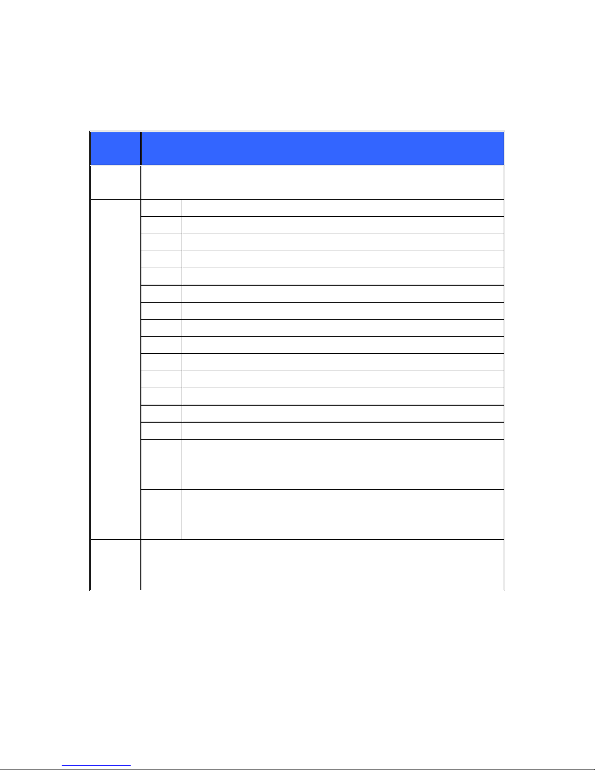
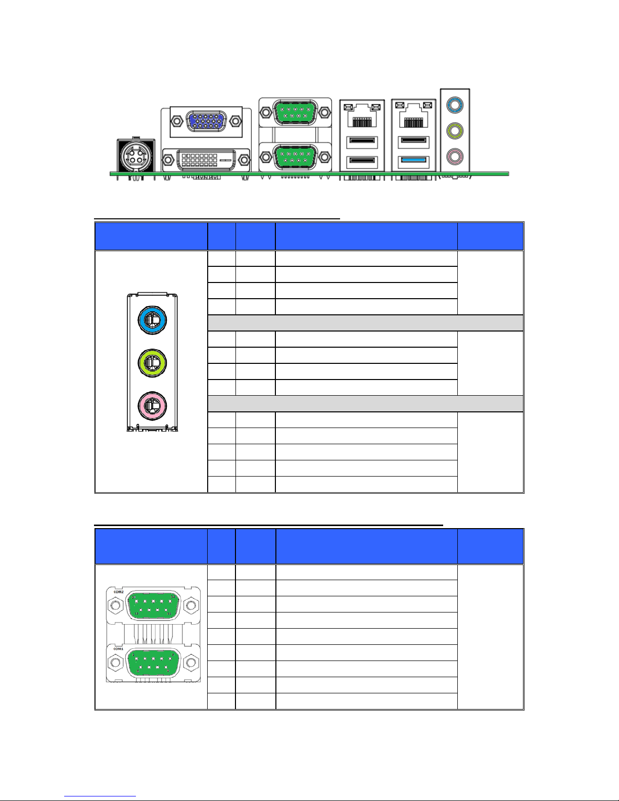
1.5 Connector Function List
Rear I/O Port List
Connector Function Note
AUDIO Line-in / Line-out / Mic-in connector
COM1_COM2 COM1, RS-232 serial port (DB9) connector
COM2, RS-232/422/485 serial port (DB9) connector
DVI-D_VGA DVI-D, DVI digital connector
VGA, VGA (DB15) connector
PWR1 DC-Jack 4pin connector (+12Vdc ~ +24Vdc)
USB1_LAN1 USB1, USB3.0 x1 / USB2.0 x1 conenctor
LAN1, RJ45 (LAN) conenctor
USB2_LAN2 USB2, USB2.0 x2 conenctor
LAN2, RJ45 (LAN) conenctor
On Board Expansion Slot List
Connector Function Note
BAT1 CMOS battery (CR2032) slot
CHA-DIMM DDR3L SO-DIMM slot
MINI-PCIE miniPCIe Express (full-size) or mSATA slot (share)
PCIE PCI Express x1 slot
MICRO-SD Micro SD / T-Flash slot
On Board I/O Connector List (1/2)
Connector Function Note
COM3, COM4,
COM5, COM6 RS-232 serial ports with box-header
CPUFAN CPU FAN 4-pin connector
DIO Digital I/O with pin-header
FP_HDA Front Panel audio with pin-header
FRONT Front Panel with pin-header
INV LCD inverter with box-header

14
On Board I/O Connector List (2/2)
Connector Function Note
KB_MS PS/2 keyboard and mouse with box-header
LVDS LCD panel LVDS 18/24bit connector
PWR2 ATX +12V 2x2 pin (4-pole) connector
SATA SATA 2.0 port connector
SATAPWR SATA power box-header (+5V and +12V)
SMB SMBus with pin-header
SYSFAN System FAN 3-pin connector
USB3, USB4 USB2.0 with pin-header
WEBCAM Webcam with box-header
LPC Reserved for debug with pin-header
SPI Reserved for debug with pin-header
15
1.6 Connector Definitions
The following sections provide pin definitions and detailed description of all on-board
connectors. The connector definitions follow the following notation:
Column
Name Description
Pin Shows the pin-numbers in the connector. The graphical layout of the
connector definition tables is made similar to the physical connectors.
Type Al Analogue Input.
AO Analogue Output.
I Input, TTL compatible if nothing else stated.
IO Input / Output TTL compatible if nothing else stated.
IOT Bi-directional tri-state IO pin.
IS Schmitt-trigger input, TTL compatible.
IOC Input/open-collector Output, TTL compatible.
IOD Input / Output, CMOS level Schmitt-triggered (open drain output).
NC Pin not connected.
O Output, TTL compatible.
OC Output, open-collector or open-drain, TTL compatible.
OT Output with tri-state capability, TTL compatible.
DIFF Differential Signal.
PWR Power supply or ground reference pins.
IOH
Typical current in mA flowing out of an output pin through a
grounded load, while the output voltage is > 2.4 V DC (if nothing
else stated).
IOL
Typical current in mA flowing into an output pin from a VCC
connected load, while the output voltage is < 0.4 V DC (if nothing
else stated).
Signal The mnemonic name of the signal at the current pin. The notation “XX#”
states that the signal “XX” is active low.
Note Special remarks concerning the signal.
※The abbreviation TBD is used for specifications which are not available yet or which are
not sufficiently specified by the component vendors.
16
Rear I/O Port Pin Define
AUDIO: Line-in / Line-out / MIC-in Connectors
AUDIO Pin Type Signal Note
32 AI Line-in (Left) Phone Jack
LINE-IN
(Blue)
33 PWR Ground
34 AI Line-in (Detect)
35 AI Line-in (Right)
22 AI Line-out (Left) Phone Jack
LINE-OUT
(Green)
23 PWR Ground
24 AI Line-out (Detect)
25 AI Line-out (Right)
1 PWR Audio shield ground
Phone Jack
MIC-IN
(Pink)
2 AI Mic-in (Left)
3 PWR Ground
4 AI Mic-in (Detect)
5 AI Mic-in (Right)
COM1_COM2: RS-232/422/485 Serial Port (DB9) Connectors (1/2)
COM1_COM2 Pin Type Signal
RS‐232|RS‐422|RS485 Note
10 I
Data Carrier Detect (DCD) |TX D-|DATA‐
COM2
(UP)
RS-232
RS-422
RS-485
Pin.18 by
jumper
select
11 I
Received Data (RXD) |TX D+|DATA+
12 O
Transmitted Data (TXD) |RX D+
13 O
Data Terminal Ready (DTR)|RX D-
14 PWR Ground
15 I Data Set Ready (DSR)
16 O Request To Send (RTS)
17 I Clear To Send (CTS)
18 I/PWR Ring Indicator (RI#) / +5V / +12V
Note 1: COM1 port pin.9 and COM2 port pin.18 function by jumper select RI# / +5V / +12V.
Note 2: COM1 port pin.9 and COM2 port pin.18 power supply maximum +5V/1.0A or +12V/1.0A
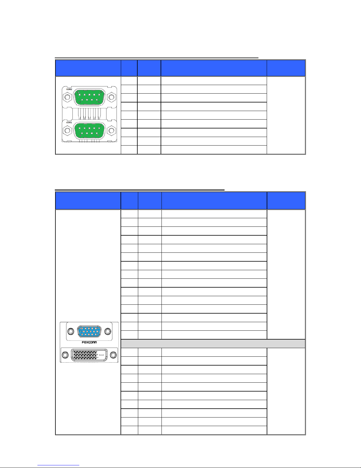
17
COM1_COM2: RS-232/422/485 Serial Port (DB9) Connectors (2/2)
COM1_COM2 Pin Type Signal Note
1 I Data Carrier Detect
(
DCD
)
COM1
(DOWN)
RS-232
Pin.9 by
jumper
select
2 I Received Data
(
RXD
)
3 O Transmitted Data
(
TXD
)
4 O Data Terminal Read
y
(
DTR
)
5 PWR Ground
6 I Data Set Read
y
(
DSR
)
7 O Request To Send
(
RTS
)
8 I Clear To Send
(
CTS
)
9 I/PWR Rin
g
Indicator
(
RI#
)
/
+5V
/
+12V
Note 1: COM1 port pin.9 and COM2 port pin.18 function by jumper select RI# / +5V / +12V.
Note 2: COM1 port pin.9 and COM2 port pin.18 power supply maximum +5V/1.0A or +12V/1.0A
DVI-D_VGA: DVI digital / VGA (DB15) Connectors (1/2)
DVI-D_VGA Pin Type Signal Note
R1
A
O VGA Red colour values
VGA
(UP)
R2
A
O VGA Green colour values
R3
A
O VGA Blue colour values
R4 NC Not connected
R5 PWR Ground
R6 PWR Ground
R7 PWR Ground
R8 PWR Ground
R9 PWR VG
A
power +5V
R10 PWR Ground
R11 NC Not connected
R12 IO VGA DDC data
R13 O VGA Horizontal s
y
nchronization
R14 O VGA Vertical s
y
nchronization
R15 IO VGA DDC clock
1 DIFF DVI TMDS D
A
T
A
2-
DVI-D
(DOWN)
2 DIFF DVI TMDS D
A
T
A
2+
3 PWR DVI TMDS D
A
T
A
2
/
4 shield
g
round
4 NC Not connected
5 NC Not connected
6 IO DVI DDC clock
7 IO DVI DDC data
8 NC Not connected
9 DIFF DVI TMDS D
A
TA1-
10 DIFF DVI TMDS D
A
T
A
1+

18
DVI-D_VGA: DVI Digital / VGA (DB15) Connectors (2/2)
DVI-D_VGA Pin Type Signal Note
11 PWR DVI TMDS D
A
TA1/3 shield
g
round
DVI-D
(DOWN)
12 NC Not connected
13 NC Not connected
14 PWR DVI power +5V
15 PWR Ground
16 I
DVI Hot
p
lu
g
detect
17 DIFF DVI TMDS D
A
T
A
0-
18 DIFF DVI TMDS D
A
TA0+
19 PWR DVI TMDS D
A
TA0/5 shield
g
round
20 NC Not connected
21 NC Not connected
22 PWR DVI TMDS Clock shield
g
round
23 DIFF TMDS CLOCK+
24 DIFF TMDS CLOCK-
Note 1: DVI-D port pin.6 (DDC Clock) and pin.7 (DDC Data) Pull Up +3.3V/2.2KΩ.
PWR1: DC-Jack 4-Pin Connector
PWR1 Pin Type Signal Note
1 PWR Ground
2 PWR Ground
3 PWR DC-IN +12Vdc ~ +24Vdc 1
4 PWR DC-IN +12Vdc ~ +24Vdc 1
Note 1: PWR1 support power adapter +12Vdc ~ +24Vdc ±10%
USB1_LAN1: USB3.0 x1 / USB2.0 x1 / RJ45 (LAN) Connectors (1/2)
USB1_LAN1 Pin Type Signal Note
20 DIFF MDI0+
/
TXD+
LAN1
(UP)
21 DIFF MDI0-
/
TXD-
22 DIFF MDI1+
/
RXD+
23 DIFF MDI2+
24 DIFF MDI2-
25 DIFF MDI1-
/
RXD-
26 DIFF MDI3+
27 DIFF MDI3-
10 PWR USB2.0 P1 power +5V
USB2.0
(Middle)
11 DIFF USB2.0 P1
_
D+
12 DIFF USB2.0 P1
_
D-
13 PWR Ground

19
USB1_LAN1: USB3.0 x1 / USB2.0 x1 / RJ45 (LAN) Connectors (2/2)
USB1_LAN1 Pin Type Signal Note
1 PWR USB3.0 P0 power +5V
USB 3.0
(DOWN)
(Blue)
2 DIFF USB2.0 P0_D+
3 DIFF USB2.0 P0_D-
4 PWR Ground
5 DIFF USB3.0 P0_RX-
6 DIFF USB3.0 P0_RX+
7 PWR Ground
8 DIFF USB3.0 P0_TX-
9 DIFF USB3.0 P0_TX+
Note 1: USB 2.0 Port power supply maximum +5V/0.5A
Note 2: USB 3.0 Port power supply maximum +5V/0.9A
USB2_LAN2: USB2.0 x2 / RJ45 (LAN) Connectors
USB2_LAN2 Pin Type Signal Note
L2 DIFF MDI0+ / TXD+
LAN2
(UP)
L3 DIFF MDI0- / TXD-
L4 DIFF MDI1+ / RXD+
L5 DIFF MDI2+
L6 DIFF MDI2-
L7 DIFF MDI1- / RXD-
L8 DIFF MDI3+
L9 DIFF MDI3-
U5 PWR USB2.0 P3 power +5V
USB 2.0
(MIDDLE)
U6 DIFF USB2.0 P3_D+
U7 DIFF USB2.0 P3_D-
U8 PWR Ground
U1 PWR USB2.0 P2 power +5V
USB 2.0
(DOWN)
U2 DIFF USB2.0 P2_D+
U3 DIFF USB2.0 P2_D-
U4 PWR Ground
Note 1: USB 2.0 ports power supply maximum +5V/0.5A

20
OnBoard Expansion Slot Pin Define
BAT1: COMS Battery Slot
BAT1 Pin Type Signal Note
1 PWR CR2032 Lithium Manganese Battery
+2.5V~+3.3V
2 PWR Ground
3 PWR CR2032 Lithium Manganese Battery
+2.5V~+3.3V
CHA-DIMM: DDR3L SO-DIMM Slot (1/3)
Signal Type Pin CHA-DIMM Pin Type Signal
VREF
_
DQ IO 1 2 PWR Ground
Ground PWR 3 4 IO DQ4
DQ0 IO 5 6 IO DQ5
DQ1 IO 7 8 PWR Ground
Ground PWR 9 10 DIFF DQS0#
DM0 I 11 12 DIFF DQS0
Ground PWR 13 14 PWR Ground
DQ2 IO 15 16 IO DQ6
DQ3 IO 17 18 IO DQ7
Ground PWR 19 20 PWR Ground
DQ8 IO 21 22 IO DQ12
DQ9 IO 23 24 IO DQ13
Ground PWR 25 26 PWR Ground
DQS1# DIFF 27 28 I DM1
DQS1 DIFF 29 30 I Reset#
Ground PWR 31 32 PWR Ground
DQ10 IO 33 34 IO DQ14
DQ11 IO 35 36 IO DQ15
Ground PWR 37 38 PWR Ground
DQ16 IO 39 40 IO DQ20
DQ17 IO 41 42 IO DQ21
Ground PWR 43 44 PWR Ground
DQS2# DIFF 45 46 I DM2
DQS2 DIFF 47 48 PWR Ground
Ground PWR 49 50 IO DQ22
DQ18 IO 51 52 IO DQ23
DQ19 IO 53 54 PWR Ground
Ground PWR 55 56 IO DQ28
Table of contents
Other CJB Motherboard manuals


