UG-1151 EVAL-AD5761RSDZ User Guide
Rev. 0 | Page 4 of 17
POWER SOLUTION (ADP5070)—SINGLE-SUPPLY
OPTION
The EVAL-AD5761RSDZ is populated with an ADP5070 switching
regulator. This regulator is preceded by voltage regulators
(ADP7142, ADP7182) that can be bypassed if required. The
supplies generated from the ADP5070 alone or with the addition of
the voltage regulators are −11 V and +21.1 V from a single supply
as low as +3 V. These generated voltages allow the AD5761R to
output any of the eight available ranges within the DAC. Note
that Link LK7 and Link LK8 must be inserted when the voltage
regulators are bypassed to avoid surpassing the absolute
maximum ratings of the AD5761R DAC.
The circuit was designed using the Analog Devices®
ADIsimPower™ toolset, which selects the components and
generates the schematic and bill of materials, and displays the
performance specifications. Visit the ADP5070 product page to
download the design tools.
The ADP5070 requires a minimum voltage supply of 3 V for
correct operation. Following the jumper configuration in Table 1
for the on-board ADP5070 or the ADP5070 with low dropout
regulators (LDOs) options, the board can be supplied in three
alternative ways: external 3 V to 15 V single supply, USB port
supply, and SDP-B controller board supply.
External 3 V to 15 V Single Supply
The EVAL-AD5761RSDZ board is supplied with a voltage in the
range of 3 V to 15 V, via the PVIN_3V–15V connector.
Note that Link LK2 must be removed for the power supply to be
driving the minimum 3 V. Also note that Link LK14 must be
removed to enable both the positive and negative outputs on the
ADP5070. See Table 2 for full link options.
USB Port Supply
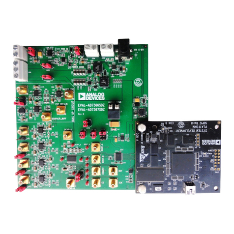
The EVAL-AD5761RSDZ is supplied through the USB_POWER
connector via a USB mini-B cable. No extra voltage supplies are
required for the board to operate.
Note that the LK2 link must be removed for the USB port to be
the only supply source. Also note that Link LK14 must be
removed to enable both the positive and negative outputs on the
ADP5070. Refer to Table 2 for full link options.
SDP-B Controller Board Supply
Alternatively, the EVAL-AD5761RSDZ can be supplied with 5 V
coming from the Blackfin® on the SDP-B board.
Note that Link LK2 must be inserted for the 5 V supply to be
available on the EVAL-AD5761RSDZ. Also note that Link LK14
must be removed to enable both positive and negative outputs
on the ADP5070. Refer to Table 2 for full link options.
BENCH POWER SUPPLY—DUAL-SUPPLY OPTION
The EVAL-AD5761RSDZ can be powered using a bench supply
to allow all output voltage ranges of the AD5761R. A headroom
and footroom of at least 1 V is required on the dual supply. It is
important that the voltage across VDD to VSS does not exceed the
absolute maximum rating of 34 V. Otherwise, device reliability
may be affected.
Following the jumper configuration in Table 1 for the bench
supply or bench supply with LDOs options, supply the board
with a dual supply of −Vs = −11 V and +Vs = +21 V via the
J4 connector.
Note that Link LK14 must be inserted to disable both positive and
negative outputs on the ADP5070. This configuration avoids
any possible noise to be coupled to the power solution when a
supply is simultaneously applied to the ADP5070 switching
regulator. Refer to Table 2 for full link options.
