Evaluation Kit User Manual for FX818, FX828 and FX829 EV8000
1997Consumer Microcircuits Limited 10 UM8000/3
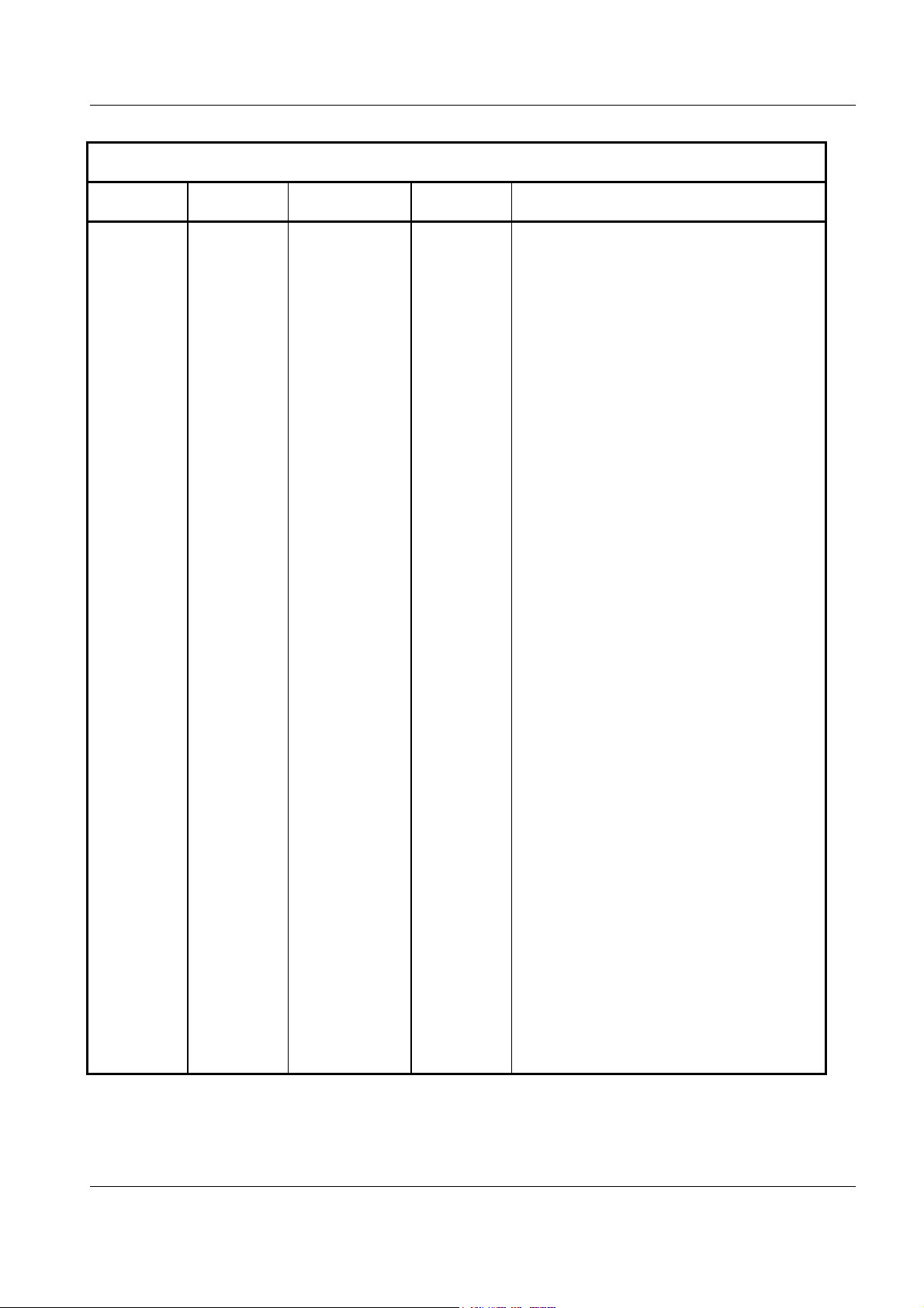
CONNECTOR PINOUT - µµC BOARD
Connector
Ref. Connector
Pin No. Signal
Name Signal
Type Description
J1 1, 2 VIN Power +ve power from external power supply.
3, 4 VSS Power 0V power from external power supply.
5RA0 BI PIC µC Bidirectional Port, pin 2
6RA1 BI PIC µC Bidirectional Port, pin 3
7RA2 BI PIC µC Bidirectional Port, pin 4
8RA3 BI PIC µC Bidirectional Port, pin 5
9RB0 BI PIC µC Bidirectional Port, pin 33
10 RB1 BI PIC µC Bidirectional Port, pin 34
11 RB2 BI PIC µC Bidirectional Port, pin 35
12 RB3 BI PIC µC Bidirectional Port, pin 36
13 RB4 BI PIC µC Bidirectional Port, pin 37
14 RB5 BI PIC µC Bidirectional Port, pin 38
15 RB6 BI PIC µC Bidirectional Port, pin 39
16 RB7 BI PIC µC Bidirectional Port, pin 40
17 RC0 BI PIC µC Bidirectional Port, pin 15
18 RC1 BI PIC µC Bidirectional Port, pin 16
19 RC2 BI PIC µC Bidirectional Port, pin 17
20 RC3 BI PIC µC Bidirectional Port, pin 18
J2 1RA4 BI PIC µC Bidirectional Port, pin 6
2RA5 BI PIC µC Bidirectional Port, pin 7
3RD0 BI PIC µC Bidirectional Port, pin 19
4RD1 BI PIC µC Bidirectional Port, pin 20
5RD2 BI PIC µC Bidirectional Port, pin 21
6RD3 BI PIC µC Bidirectional Port, pin 22
7RD4 BI PIC µC Bidirectional Port, pin 27
8RD5 BI PIC µC Bidirectional Port, pin 28
9RD6 BI PIC µC Bidirectional Port, pin 29
10 RD7 BI PIC µC Bidirectional Port, pin 30
11 RE0 BI PIC µC Bidirectional Port, pin 8
12 RE1 BI PIC µC Bidirectional Port, pin 9
13 RE2 BI PIC µC Bidirectional Port, pin 10
14 to 18 inc - - Not used. No connection needed.
19, 20 VSS Power 0V power from external power supply.