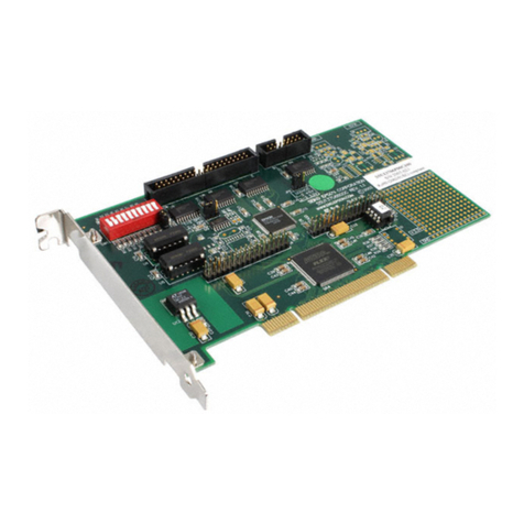
Commell LP-150 User manual

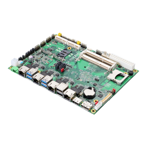
LP-150
ARM Pico-ITX Motherboard
User’s Manual
Edition 1.2
2018/05/21

LP-150 User’s Manual
-1-
Copyright
Copyright 2017, all rights reserved. This document is copyrighted and all rights are reserved.
The information in this document is subject to change without prior notice to make
improvements to the products.
This document contains proprietary information and protected by copyright. No part of this
document may be reproduced, copied, or translated in any form or any means without prior
written permission of the manufacturer.
All trademarks and/or registered trademarks contains in this document are property of their
respective owners. Disclaimer
The company shall not be liable for any incidental or consequential damages resulting from
the performance or use of this product.
The company does not issue a warranty of any kind, express or implied, including without
limitation implied warranties of merchantability or fitness for a particular purpose.
The company has the right to revise the manual or include changes in the specifications of
the product described within it at any time without notice and without obligation to notify any
person of such revision or changes.
Trademark
All trademarks are the property of their respective holders.
Any questions please visit our website at TUhttp://www.commell.com.twUT

LP-150 User’s Manual
-2-
Packing List:
Please check the package content before you starting using the board.
Optional:
1 x LP-150 Motherboard
1 xDC Input Power Cable
(OALDC-B / 1040513)
1 x Audio cable
(OALPJ-HDUNB / 1040123)
1 x Dual COM cable
(OALES-BKU2NB / 1040090)
+
_

LP-150 User’s Manual
-3-
Index
Chapter 1 <Introduction> .............................................. 4
1.1 <Product Overview> .............................................................................................4
1.2 <Product Specification>........................................................................................5
1.3 <Block Diagram>...................................................................................................6
Chapter 2 <Hardware setup> ........................................ 7
2.1 <Connector Location and Reference> ..................................................................7
2.1.1 <Internal connectors list> ........................................................................8
2.1.2 <External connectors list> ........................................................................8
2.2 <I/O Interface> .....................................................................................................9
2.2.1 <Audio Interface>.....................................................................................9
2.2.2 <Debug Interface>..................................................................................10
2.2.3 <RTC Interface> ......................................................................................10
2.2.5 <Expend GPIO Interface> .......................................................................11
2.2.6 <UART Interface> ...................................................................................12
2.2.7 <RS-232 Interface>.................................................................................13
2.2.8 <Push Button>........................................................................................14
2.2.9 <CVBS Interface>....................................................................................14
2.2.10 <Touch Panel Interface>.......................................................................15
2.2.11 <FPC Touch Interface> Shared with J27 ...............................................15
2.2.12 <LVDS Interface> ..................................................................................16
2.2.13 <FPC LCD Inverter Interface> Shared with J35 .....................................17
2.2.14 <LCD Inverter Interface> ......................................................................18
2.2.15 <Power supply>....................................................................................19
Contact information..................................................... 20

LP-150 User’s Manual
-4-
Chapter 1 <Introduction>
1.1 <Product Overview>
LP-150 is a Pico motherboard that based on Rockchip RK3128 high performance
Quad-core application processor to implement most useful features and functionalities of
this integrated processor. This motherboard is designed to be a development board for
customers to implement and verify their applications for RK3128 features.
The RK3128 Quad-core Cortex-A7 is integrates with separately Neon and FPU coprocessor,
also shared 256KB L2 Cache. Mali400 MP2 GPU is embedded to support smoothly
high-resolution (1080p) display and mainstream game.
Lots of high-performance interface to get very flexible solution, such as multi-pipe display
with HDMI1.4, TV Encoder. Crypto hardware is integrated for support security BOOT. 32bits
DDR3/LPDDR2 provides high memory bandwidths for high-performance.
The device enables OEMs and ODMs to quickly bring to market devices featuring robust
operating systems support, rich user interfaces, and high processing performance life
through the maximum flexibility of a fully integrated mixed processor solution.
The Cortex-A7 processor builds on the energy-efficient 8-stage pipeline of the Cortex-A5
processor. It also benefits from an integrated L2 cache designed for low-power, with lower
transaction latencies and improved OS support for cache maintenance. On top of this there
is improved branch prediction and an improved memory system performance, with 64-bit
load-store path, 128-bit AMBA4 AXI buses and increased TLB size (256 entry, up from 128
entry for Cortex-A9 and Cortex-A5), increasing performance for large workloads such as
web browsing.
In a 28nm process, the Cortex-A7 can run at 1.2-1.6GHz, has an area of 0.45mm2 (with
Floating-Point Unit, NEON and a 32KB L1 cache) and requires less than 100mW of total
power in typical conditions. This lowest performance profile makes it an ideal standalone
processor for a range of mobile devices, and means the Cortex-A7 can ultimately deliver
similar performance to the Cortex-A9 processor at much higher levels of power efficiency.
LP-150 User’s Manual
-5-
1.2 <Product Specification>
System
Processor
Rockchip RK3128 Quad-core Cortex-A7
Speed
Memory
512MB DDR3
Real Time Clock
Integrated RTC onboard
GPU
Mali400 MP2 GPU is embedded
Display
HDMI
Integrated HDMI 1.4 output up to 1080P
Display
Default 1024x600 LVDS LCD panel
Display Interface
Default Capacitive 1024x600 touch screen
Software
OS
Compatible with Android 4.4.4
I/O
Flash Support
1 x 8GB onboard eMMC, 1 x Micro SD card slot
Audio
Rk3128 Built-in Stereo Audio CODEC
LAN
RTL8211E Ethernet Transceiver
Internal I/O
1 x Pin header for RS232 x 2, 1 x Pin header for UART x 3
1 x LVDS panel connector, 1 x LVDS inverter connector,
1 x Pin header for expand GPIO, 1 x RTC battery
1 x Audio pin header for line-out and MIC-in
1 x system reset, power LED
External I/O
1 x Micro SD card slot, 1 x HDMI port, 1 x USB Host 2.0 ports
1 x USB OTG 2.0 port, 1 x RJ-45 LAN port, 1 x CVBS Input
1 x 5V DC-in power
Mechanical & Environmental
Power Requirement
DC INPUT 5V
Size & Thickness
100mm x 72mm (L x W)
Temperature
Operating within 0°C~70°C (32°F~158°F)
Storage within -20°C~80°C (-4°F~176°F)
Relative Humidity
10%~90%, non-condensing

LP-150 User’s Manual
-6-
1.3 <Block Diagram>
CPU
Apollo Lake
SoC
HDMI
HDMI
LVDS
TP+INV
USB HOST
USB OTG
Micro SD
WIFI
ETHERNET
LVDS
AP6181
AP6181
RTL8211E
POWER
HOST
OTG
RTC Battery
CVBS IN
COM x2
(RS232)
UART x3
ADV7180
WK2204
SP3223
CIF
UABT0
UART0
UART1
AUDIO
EX GPIO
SN7325
I2C0
Main board

LP-150 User’s Manual
-7-
Chapter 2 <Hardware setup>
2.1 <Connector Location and Reference>
(J40) AUDIO
(J21) 5V_IN
(J27) TOUCH
(J35) LVDS
(J28) Debug
(J38) UART
(J36) RS232
(J24) RTC Header
(SW3) RESET
(SW5) PWR_KEY
(J2) OTG
(J10) LCD
(J32) TOUCH
(J26) INV
(U16) RTC-Holder
Top View
Bottom View
(J41) EX_GPIO
(J22) AV IN

LP-150 User’s Manual
-8-
2.1.1 <Internal connectors list>
Connector
Function
J21
2-pin power input Terminal Block (5V Only)
J22
2-pin AV IN pin header
J27
6-pin Touch panel connector
J35
20 x 2-pin LVDS connector
J40
5 x 2-pin AUDIO pin header
J38
9 x 2-pin UART pin header
J41
10 x 2-pin External IO pin header
J36
10 x 2-pin RS-232 pin header
SW5
Power button
SW3
Reset button
J24
2-pin RTC battery pin header
J28
2-pin DEBUG pin header
U16
RTC Battery holder
J10
40-pin FPC LCD panel connector
J32
6-pin FPC Touch panel connector
J26
5-pin LCD inverter connector
2.1.2 <External connectors list>
Connector
Function
J30
RJ45 LAN connector
J3
Micro SD connector
J4
HDMI connector
USB
USB Host 2.0 connector
J6202
WiFi SMAAntenna connector
J2
USB OTG 2.0 connector
(J30) LAN
(J3) Micro SD
(J4) HDMI
(USB)
USB2.0
WIFI ANT
(J6202)
Rear I/O

LP-150 User’s Manual
-9-
2.2 <I/O Interface>
2.2.1 <Audio Interface>
J40: Front panel audio 10-pin header (Pitch 1.27mm x 2.54mm)
Pin
Signal
Pin
Signal
1
MIC_IN-
2
GND
3
MIC_IN+
4
NC
5
HP_OUTR
6
NC
7
NC
8
NC
9
HP_OUTL
10
NC
J40 (AUDIO)
1
2
9
10

LP-150 User’s Manual
-10-
2.2.2 <Debug Interface>
J28: Debug 3-pin connector
2.2.3 <RTC Interface>
J24: RTC 2-pin connector (Pitch 2.54mm)
Pin
Signal
1
UART_TX
2
UART_RX
3
GND
Pin
Signal
1
3.3V
2
GND
1
3
J28 (Debug)
1
2
CR1202 Compatible
U16 (RTC-Holder)
J24 and U16 are alternative to use
J24
(RTC Header)

LP-150 User’s Manual
-11-
2.2.5 <Expend GPIO Interface>
J41: 16bits EX_GPIO 20-pin header (Pitch 1.27mm x 2.54mm)
Pin
Signal
Pin
Signal
1
EX_GPIO1
2
EX_GPIO2
3
EX_GPIO3
4
EX_GPIO4
5
EX_GPIO5
6
EX_GPIO6
7
EX_GPIO7
8
EX_GPIO8
9
EX_GPIO9
10
EX_GPIO10
11
EX_GPIO11
12
EX_GPIO12
13
EX_GPIO13
14
EX_GPIO14
15
EX_GPIO15
16
EX_GPIO16
17
VCCIO(3.3V)
18
GND
19
VCCIO(3.3V)
20
GND
J41 (EX_GPIO)
1
2
19
20

LP-150 User’s Manual
-12-
2.2.6 <UART Interface>
J38: 18-pin UART header (Pitch 1.27mm x 2.54mm)
Pin
Signal
Pin
Signal
1
UART1_RX_GPIO1_B2_SPI_RX
2
UART1_TX_GPIO1_B1_SPI_TX
3
UART1_RTS_GPIO1_B3_SPI_CSN
4
UART1_CTS_GPIO1_B0_SPI_CLK
5
GND
6
GND
7
UART_EX2_RX
8
UART_EX2_TX
9
UART_EX2_RTS
10
UART_EX2_CTS
11
GND
12
GND
13
UART_EX4_RX
14
UART_EX4_TX
15
UART_EX4_RTS
16
UART_EX4_CTS
17
GND
18
GND
J38 (UART)
1
2
17
18

LP-150 User’s Manual
-13-
2.2.7 <RS-232 Interface>
J36: 20-pin RS232 header (Pitch 1.27mm x 2.54mm)
Pin
Signal
Pin
Signal
1
NC
2
232_1_RX
3
232_1_TX
4
NC
5
GND
6
NC
7
NC
8
NC
9
NC
10
NC
11
NC
12
232_2_RX
13
232_2_TX
14
NC
15
GND
16
NC
17
NC
18
NC
19
NC
20
NC
Note:
232_1_TX: direction input, from external device to RK3128.
232_2_TX: direction input, from external device to RK3128.
232_1_RX: direction output, from RK3128 to external device.
232_2_RX: direction output, from RK3128 to external device.
J36 (RS232)
1
2
19
20

LP-150 User’s Manual
-14-
2.2.8 <Push Button>
2.2.9 <CVBS Interface>
J22: 2-pin AV IN connector
SW3 (RESET)
SW5 (PWR KEY)
(J22) AV IN
1
2
Pin
Signal
1
CVBS IN
2
GND

LP-150 User’s Manual
-15-
2.2.10 <Touch Panel Interface>
2.2.11 <FPC Touch Interface> Shared with J27
Pin
Signal
1
VCCIO(3.3V)
2
GND
3
TP_INT
4
TP_RST
5
I2C0_SDA
6
I2C0_SCL
Pin
Signal
1
TP_RST
2
VCCIO(3.3V)
3
GND
4
TP_INT
5
I2C0_SDA
6
I2C0_SCL
1
6
(J27) TOUCH
J27: 6-pin Touch panel connector
(Pitch 1.25mm)
J32: 6-pin FPC Touch panel connector
(Pitch 1.25mm)
1
6
(J32) TOUCH

LP-150 User’s Manual
-16-
2.2.12 <LVDS Interface>
J35: LVDS 40-pin connector (Model: HIROSE DF13-40DP-1.25V compatible)
Pin
Signal
Pin
Signal
1
LCD_3V3
2
NC
3
NC
4
NC
5
NC
6
LVDS_0-
7
NC
8
LVDS_0+
9
NC
10
GND
11
NC
12
LVDS_1-
13
NC
14
LVDS_1+
15
NC
16
GND
17
NC
18
LVDS_2-
19
NC
20
LVDS_2+
21
NC
22
GND
23
NC
24
LVDS_CLK-
25
NC
26
LVDS_CLK+
27
NC
28
GND
29
NC
30
LVDS_3-
31
NC
32
LVDS_3+
33
NC
34
GND
35
LCD_RST
36
NC
37
LCD_STB
38
NC
39
NC
40
NC
1
40
2
39
(J35) LVDS

LP-150 User’s Manual
-17-
2.2.13 <FPC LCD Inverter Interface> Shared with J35
J10: 40-pin FPC LCD connector (Pitch 1.25mm)
(J10) LCD
40
1
Pin
Signal
1
VCOM
2
LCD_3V3
3
LCD_3V3
4
NC
5
LCD_RST
6
U_D
7
L_R
8
LCD_STB
9
GND
10
LVDS_CLK-
11
LVDS_CLK+
12
GND
13
LVDS_0-
14
LVDS_0+
15
GND
16
LVDS_1-
17
LVDS_1+
18
GND
19
LVDS_2-
20
LVDS_2+
Pin
Signal
21
GND
22
LVDS_3-
23
LVDS_3+
24
GND
25
SELB
26
GND
27
AVDD
28
GND
29
VGH
30
NC
31
NC
32
VGL
33
GND
34
NC
35
VCC_LEDK
36
VCC_LEDK
37
NC
38
NC
39
VCC_LEDA
40
VCC_LEDA

LP-150 User’s Manual
-18-
2.2.14 <LCD Inverter Interface>
J26: 5-pin LCD inverter connector (Pitch 1.25mm)
Pin
Signal
1
LCD_5V
2
LCD_3V3
3
GND
4
VCC_LEDK
5
VCC_LEDA
1
5
(J26) INV

LP-150 User’s Manual
-19-
2.2.15 <Power supply>
J21:Terminal Block 2-pin power connector
Pin
Signal
Pin
Signal
1
Power in (5V ONLY)
2
GND
1
2
(J21) 5V_IN
Table of contents
Other Commell Motherboard manuals

Commell
Commell LV-677 User manual

Commell
Commell LV-67N User manual

Commell
Commell P2LXB User manual

Commell
Commell LE-37M7 User manual

Commell
Commell LV-674 User manual

Commell
Commell LE-37N User manual

Commell
Commell LP-176 User manual

Commell
Commell LS-37B User manual

Commell
Commell LS-573 User manual

Commell
Commell LV-676 User manual

Commell
Commell LV-67N-G User manual

Commell
Commell LV-67E User manual

Commell
Commell HE-860 User manual

Commell
Commell P3SAE Series User manual

Commell
Commell AS-C76 User manual

Commell
Commell LV-677 User manual

Commell
Commell LV-672 User manual

Commell
Commell FE-97G User manual

Commell
Commell LE-37I User manual

Commell
Commell Mini-ITX Motherboard LV-671 User manual