Computex FP-40 Manual

On-board Flash Programmer
FP-40 Technical Information
Second Edition (Aug. 31, 2023)
Copyright ©2023 Computex Co., Ltd.
Table of Contents
Document change history...................................................................................... 1
arm Cortex series (JTAG/SWD).............................................................................. 2
■Supported connectors ................................................................................................................................ 2
■Applicable products .................................................................................................................................... 2
■FP-40 usage environment check chart....................................................................................................... 3
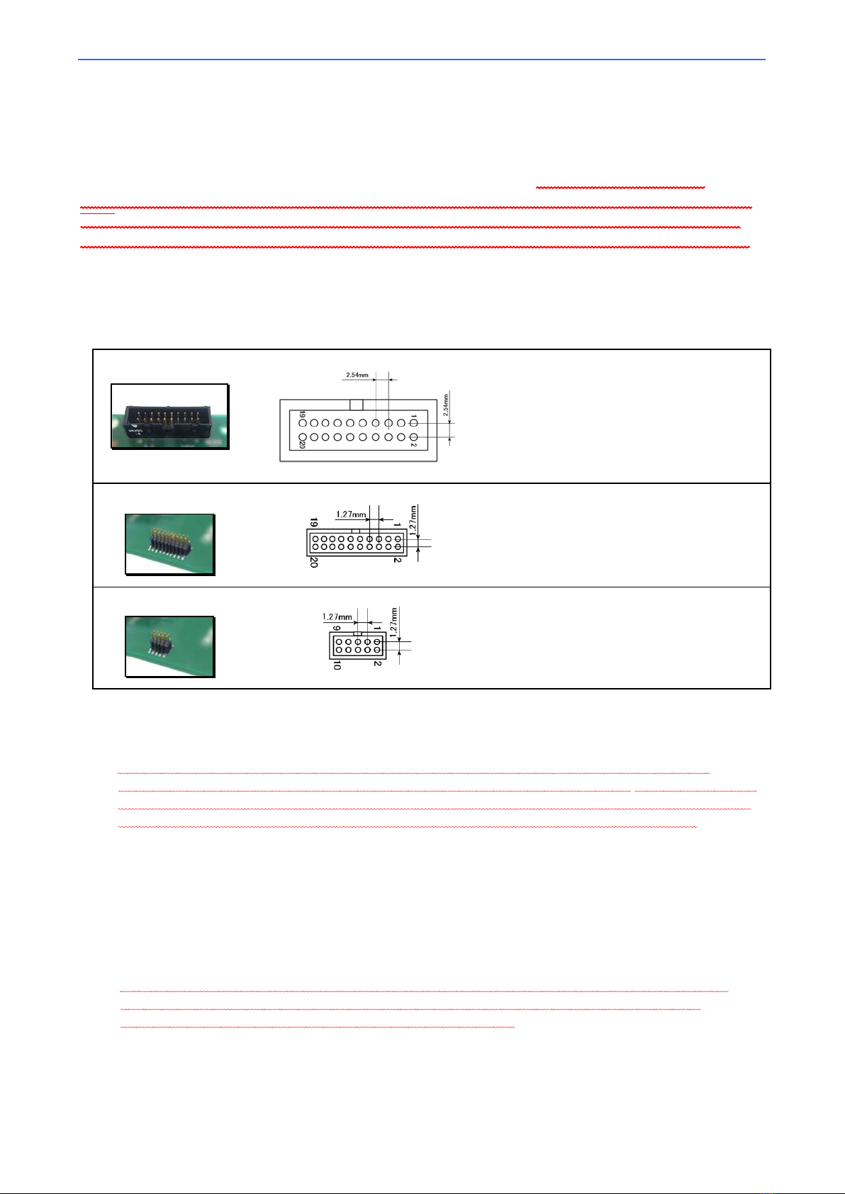
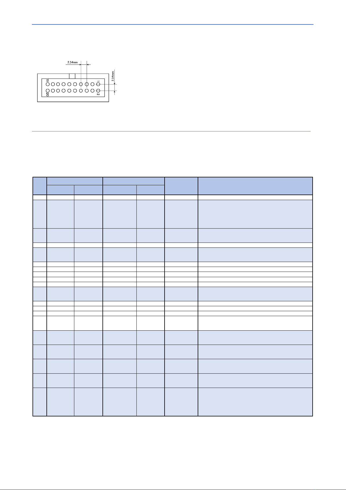
■20-pin 2.54mm-pitch connector .................................................................................................................. 4
①SWD interface ......................................................................................................................................... 4
②JTAG interface......................................................................................................................................... 6
■20-pin 1.27mm-pitch connector .................................................................................................................. 8
③SWD interface ......................................................................................................................................... 8
④JTAG interface......................................................................................................................................... 9
■10-pin 1.27mm-pitch connector ................................................................................................................ 10
⑤SWD interface ....................................................................................................................................... 10
⑥JTAG interface + Trace.......................................................................................................................... 11
■Reference:RZ/A and RZ/T series /SRST, /TRST reference diagram ....................................................... 12
■About FP-40 unique signals ..................................................................................................................... 13
Note ............................................................................................................................................................ 13
■FP-40 target interface specifications ........................................................................................................ 14
Specifications of the target connector.............................................................................................................. 14
Dimensions of TARGET cable ......................................................................................................................... 15
Target interface voltage level........................................................................................................................... 16
Signal specifications ........................................................................................................................................ 16
UART...................................................................................................................... 18
■Target interface specifications when using UART on the FP-40 unit ........................................................ 18
Specifications of the target connector.............................................................................................................. 18
Dimensions of TARGET cable ......................................................................................................................... 19
Target interface voltage level........................................................................................................................... 19
Signal specifications ........................................................................................................................................ 19
Connection reference diagram ........................................................................................................................ 20
Note................................................................................................................................................................. 20
Common specifications for each interface......................................................... 21
■External I/O functions of FP-40 ................................................................................................................ 21
External input / output function powered by VTref (1 pin)................................................................................ 21
External input / output function using 3.3V I/F ................................................................................................. 21
EX_OK/EX33_OK............................................................................................................................................ 22
EX_STARTn/EX33_STARTn ........................................................................................................................... 23
EX_BSY/EX33_BSY........................................................................................................................................ 23
EX_NG ............................................................................................................................................................ 23
Using each signal in combination .................................................................................................................... 24
External I / O function timing with VTref (1 pin)................................................................................................ 25
External I / O function timing with 3.3V I/F....................................................................................................... 25
C-Flash Settings .............................................................................................................................................. 26

1
Document change history
First Edition
Jul. 1, 2023
Initial edition
Second Edition
Aug. 31, 2023
Added description of drive specs to External I/O

Technical Information on On-board Flash Programmer FP-40 Aug. 31, 2023 (Second edition)
2
arm Cortex series (JTAG/SWD)
This section describes the specifications for connecting a CPU with a core such as Cortex-M7 or Cortex-A9 to FP-40.
The Cortex core has a dedicated debugging function called DAP. FP-40 uses this debugging function to control the CPU
to write to flash memory. SWD or JTAG is used for communication with t h e D A P. SWD is an ARM proprietary
specification that extends JTAG and uses only the TMS and TCK signals of JTAG. Also, when using JTAG, the
TRST signal may be required, or special processing may be required to use debugging functions. Please be
sure to check the CPU manual before use. This technical document describes general interface specifications.
■Supported connectors
(For detailed dimensions of the connectors, refer to the documentations by respective manufacturers of the connectors.)
20-pin 2.54mm-pitch connector
(Top view on the target board)
Recommended connector
Manufacturer: OMRON Corporation
Model : XG4C-2031
20-pin 1.27mm-pitch connector
*1
(Top view on the target board)
Recommended connector
Manufacturer: Samtec, Inc.
Model : FTSH-110-01-L-DV-K
10-pin 1.27mm-pitch connector
*2
(Top view on the target board)
Recommended connector
Manufacturer: Samtec, Inc.
Model : FTSH-105-01-L-DV-K
*1: Requires a target probe "SWJ-PRB-MIL20-20HP" (Optional product).
*2: Requires a target probe "SWJ-PRB-MIL20-10HP" (Optional product).
* Before connecting, please refer the pin configuration diagram and make sure that the
connector is in the right direction and the signals and pin numbers match. In addition to our
own specifications, each company may have extended their own specifications, so be sure to
check the signal names as well. The signal may be shorted and cause a malfunction.
■Applicable products
This manual is applicable for the following products:
On-board Flash Programmer FP-40
* FP-40 is the upgraded model of FP-10/FP-10(model PS). The interface specifications are
compatible with those of FP-10/FP-10(model PS), so existing users can replace their
FP-10/FP-10(model PS) with FP-40 without modification.

Technical Information on On-board Flash Programmer FP-40 Aug. 31, 2023 (Second edition)
3
Check the table of connector
signals.
Also consult Target connection
reference diagram.
■FP-40 usage environment check chart
The following chart table summarizes the conditions required to connect a CPU employing a Cortex core to FP-40.
With reference to the chart below, check to see if the current environment is suitable for FP-40 use.
①SWD interface
②
JTAG interface
③SWD interface
④
JTAG interface
⑤SWD interface
⑥
JTAG interface
* If you are using a CPU that requires TRST, ⑤JTAG interface cannot be used; TRST is not
provided for SWJ-PRB-MIL20-10HP.
Type of connector mounted on
the target system
20-pin 2.54mm-pitch connector
Required optional
product
No optional product required
20-pin 1.27mm-pitch connector
SWJ-PRB-MIL20-20HP
10-pin 1.27mm-pitch connector
SWJ-PRB-MIL20-10HP

Technical Information on On-board Flash Programmer FP-40 Aug. 31, 2023 (Second edition)
4
■20-pin 2.54mm-pitch connector
Target connector specifications
(Top view on the target board)
Recommended connector
Manufacturer: OMRON Corporation
Model: XG4C-2031
(For detailed dimensions of the connector, refer to the documentation by manufacturer of the connector.)
*Please refer the pin configuration diagram above and make sure that the connector is in the right direction
before connecting.
Please check the pin number in the signal table above and make sure the signal and the pin numbers
match.
①SWD interface
The SWD interface signal table when connected with a 20-pin 2.54mm pitch connector is shown below.
In addition to the standard SWD signals, a power supply function and external input/output functions are supported via
Connectionthe FP-40's unique signals. When using FP-40, refer to "About FP-40 unique signals" below for connection.
Signal description
Pin
No.
SWD I/F FP-40 FP-40 unique
Specifications Connection
Signal
Input/
Output
*1
Signal
Input/
Output
*1
1
VTref
Output
VTref
Output
-
Connect the I/O power supply of the CPU to be connected.
2 TVDD Output X3.3V
(N.C.) Input Yes
TVDD signal is not used in FP-40.
X3.3V is a FP-40 unique signal and can be used as 3.3V
power supply function.
Please note that this signal should not be used if X5V(Pin
20) is used as the power supply.
When not used, leave as NC.
3N.C. - EX_BSY
(N.C.) Input Yes
EX_BSY is a FP-40 unique signal and outputs the operation
status from FP-40.
When not used, leave as NC.
4
GND
-
GND
-
-
5N.C. - EX_NG
(N.C.) Input Yes
EX_NG is an FP-40 original signal and outputs the operation
status from FP-40.
When not used, leave as NC.
6
GND
-
GND
-
-
7
SWDIO
Input/Output
SWDIO
Input/Output
-
8
GND
-
GND
-
-
9
SWCLK
Input
SWCLK
Input
-
10
GND
-
GND
-
-
11 N.C. - EX_STARTn
(N.C.) Output Yes
EX_STARTn is a FP-40 unique signal and can be used as a
write start request signal to FP-40.
When not used, leave as NC.
12
GND
-
GND
-
-
13
SWO
Output
N.C.
-
Yes
NC as this signal is not used.
14
GND
-
GND
-
-
15 SRSTn Input SRSTn Input -
Connect the reset signal to the connected CPU with a wired
OR circuit or an OR circuit. The SRSTn signal is an open
collector output.
16 GND - EX33_BSY
(N.C.) Input Yes
EX33_BSY is an FP-40 original signal and outputs the
operation status from FP-40.
When not used, leave as NC.
17 N.C. - EX_OK
(N.C.) Input Yes
EX_OK is an FP-40 original signal and outputs the operation
status from FP-40.
When not used, leave as NC.
18 GND - EX33_OK
(N.C.) Input Yes
EX33_OK is an FP-40 original signal and outputs the
operation status from FP-40.
When not used, leave as NC.
19 N.C. - EX33_STARTn
(N.C.) Output Yes
EX33_STARTn is an FP-40 original signal and can be used
as a write start request signal to FP-40.
When not used, leave as NC.
20 GND - X5V
(N.C.) Input Yes
X5V is FP-40's unique signal and can be used as 5V power
supply function.
Cannot be used with 2-pin 3.3V power supply. If not used,
leave as NC.
Do not use as a power supply function when connected to
GND.
*1: Input/output is based on the target system.

Technical Information on On-board Flash Programmer FP-40 Aug. 31, 2023 (Second edition)
5
Signal table
Pin
No. Signal
Input/
Output
*1
Pin
No. Signal
Input/
Output
*1
1
VTref
Output
2
[X3.3V] *5
Input
3
(EX_BSY)*2
Input
4
GND
5
(EX_NG)*2
Input
6
GND
7 SWDIO
Input/
Output
8 GND
9
SWCLK
Input
10
GND
11
(EX_STARTn)*2
Output
12
GND
13
SWO*3
Output
14
GND
15
SRSTn
Input
16
<EX33_BSY>*4
Input
17
(EX_OK) *2
Input
18
<EX33_OK>*4
Input
19
<EX33_STARTn>*4
Output
20
[X5V]*5
Input
*1: Input/output is denoted for the target system.
*2:External input/output function signal that will be at VTref level when high.
This signal is not connected to the target (CPU).
*3:Unused. NC.
*4:3.3V External input/output function signal. This signal is not connected to
the target (CPU).
*5: Power supply function signal.
Target connection reference diagram
To prevent malfunction, the length of wirings from the CPU to the target connector should be kept as short as possible.
If the waveform disturbance exceeds the device specifications, suppress the disturbance by inserting a damping resistor into the signal line or use
other means.

Technical Information on On-board Flash Programmer FP-40 Aug. 31, 2023 (Second edition)
6
②JTAG interface
The JTAG interface signal table when connected with a 20-pin 2.54mm pitch connector is shown below.
In addition to the standard JTAG signal, FP-40 provides power supply function and external input/output function by
FP-40's original signal. When using FP-40, refer to "About FP-40 unique signals" below for connection.
Signal description
Pin
No.
JTAG I/F FP-40 FP-40 unique
Specifications Connection
Signal
Input/
Output
*1
Signal
Input/
Output
*1
1
VTref
Output
VTref
Output
-
Connect the I/O power supply of the CPU to be connected.
2 TVDD Output X3.3V
(N.C.) InputYes
TVDD signal is not used in FP-40.
X3.3V is a FP-40 unique signal and can be used as 3.3V
power supply function.
Please note that this signal should not be used if X5V(Pin
20) is used as the power supply.
When not used, leave as NC.
3TRST/
N.C.(Cortex-M) - TRST Input -
TRST is not used with Cortex-M core CPUs. Leave as NC.
For CPUs other than Cortex-M, please refer to the
datasheet.
4
GND
-
GND
-
-
5
TDI
Input
TDI
Input
-
6
GND
-
GND
-
-
7
TMS
Input
TMS
Input
-
8
GND
-
GND
-
-
9
TCK
Input
TCK
Input
-
10
GND
-
GND
-
-
11
N.C.
-
N.C.
-
-
12
GND
-
GND
-
-
13
TDO
Output
TDO
Output
-
14
GND
-
GND
-
-
15 SRSTn Input SRSTn Input -
Connect the reset signal to the connected CPU with a
wired OR circuit or an OR circuit. The SRSTn signal is an
open collector output.
16 GND - EX33_BSY
(N.C.) Input Yes
EX33_BSY is an FP-40 original signal and outputs the
operation status from FP-40.
When not used, leave as NC.
17
N.C.
-
N.C.
-
-
18 GND - EX33_OK
(N.C.) Input Yes
EX33_OK is an FP-40 original signal and outputs the
operation status from FP-40.
When not used, leave as NC.
19 N.C. -
EX33_START
n
(N.C.)
Output Yes
EX33_STARTn is an FP-40 original signal and can be
used as a write start request signal to FP-40.
When not used, leave as NC.
20 GND - X5V
(N.C.) Input Yes
X5V is FP-40's unique signal and can be used as 5V
power supply function.
Cannot be used with 2-pin 3.3V power supply. If not used,
leave as NC.
Do not use as a power supply function when connected to
GND.
*1: Input/output is based on the target system.

Technical Information on On-board Flash Programmer FP-40 Aug. 31, 2023 (Second edition)
7
Signal table
Target connection reference diagram
Pin
No. Signal
Input/
Output
*1
Pin
No. Signal
Input/
Output
*1
1
VTref
Output
2
[X3.3V]
*4
Input
3
TRST (N.C.)*2
Input
4
GND
5
TDI
Input
6
GND
7
TMS
Input
8
GND
9
TCK
Input
10
GND
11
N.C.*2
Output
12
GND
13
TDO
Output
14
GND
15
SRSTn
Input
16
<EX33_BSY>*3
Input
17
N.C.*2
Input
18
<EX33_OK>*3
Input
19
<EX33_STARTn>*3
Output
20
[X5V]*4
Input
*1: Input/output denoted is for the target system.
*2: TRST TRST is not used with Cortex-M core CPUs. Leave as NC. For other
CPUs, please refer to the datasheet of the CPU to be connected.
Please note that CPUs that require connection may require the signals to
be pulled-down.
Note that some CPUs manufactured by Renesas Electronics require some
precautions. Refer to "Reference:RZ/A and RZ/T series /SRST, /TRST
reference diagram" below.
*3: 3.3V External input/output function signal. This signal is not connected to
the target (CPU).
*4: Power supply function signal.
*5: Reserved for FP-40's own usage, leave as NC.
To prevent malfunction, the length of wirings from the CPU to the target connector should be kept as short as possible.
If the waveform disturbance exceeds the device specifications, suppress the disturbance by inserting a damping resistor into the signal line or use
other means.

Technical Information on On-board Flash Programmer FP-40 Aug. 31, 2023 (Second edition)
8
■20-pin 1.27mm-pitch connector
Target connector specifications
(Top view on the target board)
Recommended connector
Manufacturer: Samtec, Inc.
Model: FTSH-110-01-L-DV-K
(For detailed dimensions of the connector, refer to the documentation by manufacturer of the
connector.)
*Please refer the pin configuration diagram above and make sure that the connector is in the right direction
before connecting.
Please check the pin number in the signal table above and make sure the signal and the pin numbers
match.
This connector does not support the power supply function to the target.
③SWD interface
The signal table and target connection reference diagram when connecting a 20-pin 1.27mm pitch connector with SWD
interface are shown below.
Signal table
Pin
No. Signal
Input/
Output
*1
Pin
No. Signal Input/
Output *1
1 VTref*2 Output 2 SWDIO
Input/
Output
3
GND
4
SWCLK
Input
5
GND
6
SWO*3
Output
7
Key*6
8
NC
NC
9
GND
10
SRSTn*4
Input
11
GND*5
12
TraceClk*3
Output
13
GND*5
14
TraceD0*3
Output
15
GND
16
TraceD1*3
Output
17
GND
18
TraceD2*3
Output
19
GND
20
TraceD3*3
Output
*1
: Input/output is denoted for the target system.
*2
: Connect the I/O power supply of the CPU to VTref.
*3
: Unused. NC.
*4
: Connect the reset signal to the connected CPU with a wired
OR circuit or an OR circuit. The SRSTn signal is an open
collector output.
*5
: In some target systems, this pin may be assigned as a power
supply pin. This product is GND, so do not connect it to the
power line (or leave it unconnected).
*6
: Intended for protection against erroneous insertion.
Target connection reference diagram
To prevent malfunction, the length of wirings from the CPU to the target connector should be kept as short as possible.
If the waveform disturbance exceeds the device specifications, suppress the disturbance by inserting a damping resistor into the signal line or use
other means.

Technical Information on On-board Flash Programmer FP-40 Aug. 31, 2023 (Second edition)
9
④JTAG interface
The signal table and target connection reference diagram when connecting a 20-pin 1.27mm pitch connector with JTAG
interface are shown below.
Signal table
Pin
No. Signal Input/
Output *1
Pin
No. Signal
Input/
Output
*1
1 VTref Output 2 TMS
Input/
Output
3
GND
4
TCK
Input
5
GND
6
TDO
Output
7
Key*3
8
TDI
Input
9
GND
10
SRST*2
Input
11
GND
12
NC
13
GND
14
NC
Output
15
GND
16
TRST*4
Input
17
GND
18
NC
19
GND
20
NC
*1: Input/output is denoted for the target system.
*2: SRST is an open drain output signal.
Connect to the target system's "power-on reset" or "system reset"
with a wired OR circuit or, if a wired OR circuit is not possible, with
an OR circuit. VCC should be connected to a power supply
matching the circuitry of the target system at 5 V or less.
*3: Intended for protection against erroneous insertion.
*4:
TRST is not used with Cortex-M core CPUs. Leave as NC. For
other CPUs, please refer to the datasheet of the CPU to be
connected.
Please note that CPUs that require connection may require the
signals to be pulled-down.
Note that some CPUs manufactured by Renesas Electronics require
some precautions. Refer to "Reference:RZ/A and RZ/T series
/SRST, /TRST reference diagram " below.
Target connection reference diagram
To prevent malfunction, the length of wirings from the CPU to the target connector should be kept as short as possible.

Technical Information on On-board Flash Programmer FP-40 Aug. 31, 2023 (Second edition)
10
■10-pin 1.27mm-pitch connector
Target connector specifications
(Top view on the target board)
Recommended connector
Manufacturer:Samtec, Inc.
Model: FTSH-105-01-L-DV-K
(For detailed dimensions of the connector, refer to the documentation by manufacturer of the connector.)
*Please refer the pin configuration diagram above and make sure that the connector is in the right direction
before connecting.
Please check the pin number in the signal table above and make sure the signal and the pin numbers
match.
This connector does not support the power supply function to the target.
⑤SWD interface
The signal table and target connection reference diagram when connecting a 10-pin 1.27mm pitch connector with SWD
interface are shown below.
Signal table
Pin
No.
Signal
Input/
Output
*1
Pin
No.
Signal
Input/
Output
*1
1 VTref*2 Output 2 SWDIO
Input/
Output
3
GND
4
SWCLK
Input
5
GND
6
SWO*3
Output
7
Key*5
8
NC
Input
9
GND
10
SRSTn*4
Input
*1
: Input/output is denoted for the target system.
*2
: Connect the I/O power supply of the CPU to VTref.
*3
: Unused. NC.
*4
: Connect the reset signal to the connected CPU with a wired OR
circuit or an OR circuit. The SRSTn signal is an open collector
output.
*5
: Intended for protection against erroneous insertion.
Target connection reference diagram
To prevent malfunction, the length of wirings from the CPU to the target connector should be kept as short as possible.
If the waveform disturbance exceeds the device specifications, suppress the disturbance by inserting a damping resistor into the signal line or use
other means.

Technical Information on On-board Flash Programmer FP-40 Aug. 31, 2023 (Second edition)
11
⑥JTAG interface + Trace
The signal table and target connection reference diagram when connecting a 10-pin 1.27mm pitch connector with JTAG
interface are shown below.
Signal table
Pin
No.
Signal
Input/
Output
*1
Pin
No.
Signal
Input/
Output
*1
1 Vtref Output 2 TMS
Input/
Output
3
GND
4
TCK
Input
5
GND
6
TDO
Output
7
Key*3
8
TDI
Input
9
GND
10
SRSTn*2
Input
*1
: Input/output is denoted for the target system.
*2
: Connect the reset signal to the connected CPU with a wired OR
circuit or an OR circuit. The SRSTn signal is an open collector
output.
*3
: Intended for protection against erroneous insertion.
Target connection reference diagram
To prevent malfunction, the length of wirings from the CPU to the target connector should be kept as short as possible.
If the waveform disturbance exceeds the device specifications, suppress the disturbance by inserting a damping resistor into the signal line or use
other means.

Technical Information on On-board Flash Programmer FP-40 Aug. 31, 2023 (Second edition)
12
■Reference:RZ/A and RZ/T series /SRST, /TRST reference diagram
It may be required to control the RES and TRST CPU pins so that they are in low state at power on. Refer the CPU
datasheet for details.

Technical Information on On-board Flash Programmer FP-40 Aug. 31, 2023 (Second edition)
13
■About FP-40 unique signals
FP-40 provides unique signals to operate FP-40 from external devices such as production systems and inspection tools.
(1) can be used only with SWD interface, and (2) can be used with either SWD or JTAG interface.
(1) External I/O signals operating at Vtref
Since these signals operate with the power supply voltage of Pin1 Vtref of the target connector, they cannot
be operated unless a voltage value is supplied to Vtref. Note that when using the power supply function
described in point (3), use EX3.3_I/F described in point (2).
Signal
Description
EX_STARTn
Requests to start writing with FP-40
EX_BSY*1
Information being written is output from FP-40
EX_NG*1
Write result information is output from FP-40
EX_OK*1
Write result information is output from FP-40
*1: Level will be L if VTref is cut off.
(2) External I/O signals operating at 3.3 V inside FP-40
These are different from point (1) as these have a 3.3V dedicated I/F that uses FP-40's internal power
supply. Note that the signal corresponding to EX_NG that is in point (1) is not available. Note that the power
supply functions described in (1), (2), and (3) are independent of each other. They need not be used
simultaneously.
Signal
Description
EX33_BSY
*1
Information being written is output from FP-40
EX33_STARTn
Requests to start writing with FP-40
EX33_OK
*1
Write result information is output from FP-40
*1:Hi level is 3.3V.
(3) X3.3V, X5V for power supply
FP-40 has the ability to supply 3.3V or 5.0V power to the target system up to 200mA (simultaneous use of
3.3V and 5.0V power supplies is not possible.) An example using X3.3V power supply is shown below.
Note
FP-40 is only guarenteed to run with the dedicated cable that comes with it. Using a different cable type may lead
to unexpected results.
Keep the wire length between the JTAG connector and the CPU on the target system as short as possible.

Technical Information on On-board Flash Programmer FP-40 Aug. 31, 2023 (Second edition)
14
■FP-40 target interface specifications
This chapter describes the target interface specifications for connecting FP-40 to the target.
Specifications of the target connector
The standard interfaces supported by FP-40 are JTAG and SWD, and the connector specification is MIL 20-pin with
2.54mm pitch. Connection to the target system is made using the supplied dedicated interface cable (TARGET cable).
For interfaces other than JTAG and SWD, please refer to their individual instruction manuals.
Pin allocation
The pin allocations are specific to FP-40 and the target cable is dedicated to FP-40. Make sure that you only use
the TARGET cable that is included with the product.
Target system side
FP-40 side
Connector
FP-40 side view
Connecto to
FP-40
Target cable
FP-40

Technical Information on On-board Flash Programmer FP-40 Aug. 31, 2023 (Second edition)
15
No. Signal *1 Input/
Output *2 FP-40 internal circuit
access point
20-pin
2.54mm-pitch
20-pin
1.27mm-pitch
10-pin
1.27mm-pitch
1
VTref
Output
4KΩPull-Down
1
1
1
2 X3.3V Input Power supply
(when output is permitted)
2 - -
3
TRST / (EX_BSY)
Input
22Ωseries
3
16
-
4
GND
GND
4,6,8,10,12,14
3,5,9,11,13,15,17,19
3,5,9
5
TDI / (EX_NG)
Input
22Ωseries
5
8
8
6
GND
GND
4,6,8,10,12,14
3,5,9,11,13,15,17,19
3,5,9
7 TMS/SWDIO Input /
Input/Output
22Ωseries
10KΩPull-Up (VTref)
7 2 2
8
GND
GND
4,6,8,10,12,14
3,5,9,11,13,15,17,19
3,5,9
9
TCK/SWCLK
Input
22Ωseries
9
4
4
10
GND
GND
4,6,8,10,12,14
3,5,9,11,13,15,17,19
3,5,9
11 (EX_STARTn) Output
1KΩseries
10KΩPull-Up (VTref)
11 - -
12
GND
GND
4,6,8,10,12,14
3,5,9,11,13,15,17,19
3,5,9
13 TDO/SWO Output 22Ωseries
10KΩPull-Up (VTref)
13 6 6
14
GND
GND
4,6,8,10,12,14
3,5,9,11,13,15,17,19
3,5,9
15 SRSTn Input
100Ωseries
Open-collector output
15 10 10
16
(EX33_BSY)
Input
100Ωseries
16
3,5,9,11,13,15,17,19
3,5,9
17
(EX_OK)
Input
22Ωseries
17
-
-
18
(EX33_OK)
Input
100Ωseries
18
3,5,9,11,13,15,17,19
3,5,9
19 (EX33_STARTn) Output
1KΩseries
10KΩPull-Up (3.3V)
19 - -
20 (X5V) Input Power supply
(when output is permitted)
20 - -
*1 : Signal names in parentheses ( ) are signals with FP-40's unique specifications.
*2 : Input/Output is based on the target system.
Dimensions of TARGET cable
Dimensions of the dedicated TARGET cable are as follows.

Technical Information on On-board Flash Programmer FP-40 Aug. 31, 2023 (Second edition)
16
Target interface voltage level
Input voltage level
Target voltage (V)
5.0V
3.3V
1.8V
VIH(min)
3.5V
2.0V
1.17V
VIL(max)
1.5V
0.8V
0.63V
Output voltage level
Target voltage (V)
4.5V
3.0V
1.65V
VOH(min)
3.8V
2.4V
1.2V
VOL(max)
0.55V
0.55V
0.45V
Signal specifications
JTAG/SWD signals (TCK, TMS, TDI, TDO, SWDIO and SWCLK)
FP-40 communicates with the on-chip debug unit in the ARM core via the JTAG or SWD connections.
JTAG uses four signal lines - TCK, TMS, TDI and TDO, while SWD required two - SWDIO and SWCLK. The signal
designation may differ slightly depending on the CPU, but generally for CPUs that use both JTAG and SWD, TMS and
SWDIO, TCK and SWCLK use the same terminals.
Make sure to check the specifications of the target CPU before connecting the necessary signals.
Please note that TRST (reset signal for JTAG) is not used.
SRST signal
SRST signal is used as the reset signal for initializing the CPU from FP-40.
The output from FP-40 is open-collector to allow wired-OR connections on the power-on-reset and system reset signals
on the target.
Please refer to the CPU datasheet, etc., as the CPU may have its own extensions. Please be especially careful with
Renesas CPUs.
TRST signal
Reset signal to initialize the CPU JTAG from FP-40.
If SWD is used, there is no need to connect this signal. Also, with Cortex-M core CPUs, even if you are using JTAG, you
do not need to connect TRST.
Please refer to the CPU datasheet, etc., for TRSTconnections, as they may have been uniquely extended by the CPU.
Please be especially careful with Renesas CPUs. The output from the FP-40 is an open collector output to allow wired
OR with the target system's power-on reset or system reset signal.
Since the TRSTsignals of SWJ-PRB-MIL20-10HP and FP-40 are not connected, it is necessary to make your own cable
for "10-pin connector 1.27mm pitch" connection on CPUs that require TRST.
VTref signal
Connect the CPU's I/O power to this signal. The valid range should be 1.65V~5.5V.
FP-40 communicates at a signal level that follows the potential connected to this signal. However, some of FP-40 unique
signals are 3.3V dedicated I/F. For specifications, refer to "External I/O functions of FP-40".

Technical Information on On-board Flash Programmer FP-40 Aug. 31, 2023 (Second edition)
17
X3.3V/X5V power supply
This can be used as the power supply from FP-40 to the target system. The two pins of the target connector are X3.3V
(3.3V) and the 20 pins are X5V (5V), both of which guarantee ±5% accuracy and can supply up to 200mA. The rise time
upon power-on is 2ms. 3.3V or 5V can be used depending on the C-Flash setting, but they can't be used simultaneously.
For details on the settings, refer to "4.3 Target Settings" in "Onboard Flash Memory Programmer FP User's Manual".
These power supplies are equipped with a protection circuit that cuts the power supply if an overcurrent is detected due
to a short circuit on the target. To confirm that power is normally supplied to the target, the voltage of VTref is measured
by software processing after power is supplied, and if the voltage of VTref is lower than the [minimum input voltage of
VTref (Pin 1)], the power output is stopped to protect FP-40 itself.
If these pins are not used, leave them as NC.
External I/O function signals
These signals are for the FP-40's external I/O functions. EX_BSY, EX_NG, EX_STARTn, EX_OK, EX33_BSY, EX33_OK,
and EX33_STARTn are assigned to the target connector respectively. The target connector signals are normally
connected to the target system in which the CPU to be written is mounted, but these signals are intended to be
connected to an external production system or other controller device that controls FP-40. Please refer to “External I/O
functions of FP-40” for detailed specifications.
If the External I/O functions of FP-40 is not used, leave these signals as NC.
The specifications are the same as those of the conventional FP-10 model.

Technical Information on On-board Flash Programmer FP-40 Aug. 31, 2023 (Second edition)
18
UART
A dedicated cable is not provided to use UART.
Refer to the interface specifications below to connect to the target.
■Target interface specifications when using UART on the FP-40 unit
This section describes the interface specifications on the FP-40 unit for connecting the FP-40 to a UART on the target on the.
Specifications of the target connector
Pin allocation
No. Signal *1 Input/
Output
*2
FP-40 internal circuit
access point
20-pin 2.54mm-pitch
1
VTref
Output
4KΩPull-Down
1
2 X3.3V Input Power supply
(when output is permitted)
2
3
N.C.
Input
22Ωseries
3
4
GND
GND
4,6,8,10,12,14
5
N.C.
Input
22Ωseries
5
6
GND
GND
4,6,8,10,12,14
7 TXD Input 22Ωseries
10KΩPull-Up (VTref)
7
8
GND
GND
4,6,8,10,12,14
9
RXD
Output
22Ωseries
9
10
GND
GND
4,6,8,10,12,14
11 N.C. Output
1KΩseries
10KΩPull-Up (VTref)
11
12
GND
GND
4,6,8,10,12,14
13 N.C. Output 22Ωseries
10KΩPull-Up (VTref)
13
14
GND
GND
4,6,8,10,12,14
15 SRSTn Input
100Ωseries
Open-collector output
15
16
(EX33_BSY)
Input
100Ωseries
16
17
(EX_OK)
Input
22Ωseries
17
18
(EX33_OK)
Input
100Ωseries
18
19 (EX33_STARTn) Output
1KΩseries
10KΩPull-Up (3.3V)
19
20 (X5V) Input Power supply
(when output is permitted)
20
*1 : Signal names in parentheses ( ) are signals with FP-40's unique specifications.
*2 : Input/Output is based on the target system.
Target system side
FP-40 side
Connector
FP-40 side view
Connecto to
FP-40
Target cable
FP-40

Technical Information on On-board Flash Programmer FP-40 Aug. 31, 2023 (Second edition)
19
Dimensions of TARGET cable
Dimensions of the dedicated TARGET cable are as follows.
Target interface voltage level
Input voltage level
Target voltage (V)
5.0V
3.3V
1.8V
VIH(min)
3.5V
2.0V
1.17V
VIL(max)
1.5V
0.8V
0.63V
Output voltage level
Target voltage (V)
4.5V
3.0V
1.65V
VOH(min)
3.8V
2.4V
1.2V
VOL(max)
0.55V
0.55V
0.45V
Signal specifications
RXD/TXD signals
UART RXD/TXD signals.
Data is transmitted by FP-40 via TXD signal line.
Data is received by FP-40 via RXD signal line.
SRST signal
SRST signal is used as the reset signal for initializing the CPU from FP-40.
The output from FP-40 is open-collector to allow wired-OR connections on the power-on-reset and system reset signals
on the target.
VTref signal
Connect the CPU's I/O power to this signal. The valid range should be 1.65V~5.5V.
FP-40 communicates at a signal level that follows the potential connected to this signal. However, some of FP-40 unique
signals are 3.3V dedicated I/F. For specifications, refer to "External I/O functions of FP-40".
Table of contents
Other Computex Motherboard manuals