Concept2 1SC2060P User guide

1SC2060P
Preliminary
IGBT-Driver.com Page 1
1SC2060P Description & Application Manual
Single-Channel High-Power and High-Frequency SCALE-2 Driver Core
Abstract
The 1SC2060P is a 20W, 60A SCALE-2 driver core. It is designed for high-power and high-frequency IGBT and
MOSFET applications such as induction heating, resonant and high-frequency power conversion as well as
parallel gate driving of large modules.
The 1SC2060P features newly developed planar transformer technology for a real leap forward in power
density, noise immunity, and reliability.
With its extremely compact outline of 44mm x 74mm and a total height of typ. 6.5mm, the driver delivers high
power density with an attractive form factor. The component count is reduced by 80% compared to
conventional solutions thanks to the highly integrated SCALE-2 chipset. This results in significantly increased
reliability and reduced costs.
Fig. 1 1SC2060P driver core

1SC2060P
Description and Application Manual
Page 2 INTELLIGENT POWER ELECTRONICS
Contents
Abstract.......................................................................................................................................... 1
Contents......................................................................................................................................... 2
Driver Overview ............................................................................................................................. 4
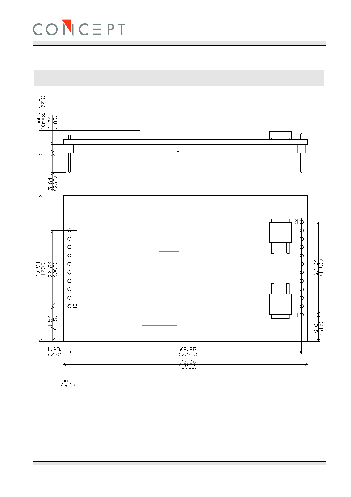
Mechanical Dimensions.................................................................................................................. 5
Pin Designation .............................................................................................................................. 6
Recommended Interface Circuitry for the Primary Side Connector .............................................. 7
Description of Primary Side Interface ........................................................................................... 7
General .................................................................................................................................7
VCC terminal .........................................................................................................................7
VDC terminal .........................................................................................................................7
IN (drive input, e.g. PWM) .....................................................................................................8
SO (status output) .................................................................................................................8
TB (input for adjusting the blocking time Tb) ...........................................................................8
Recommended Interface Circuitry for the Secondary Side Connector .......................................... 9
Description of Secondary Side Interface .....................................................................................10
General ............................................................................................................................... 10
DC/DC output (VISO), emitter (VE) and COM terminals
.......................................................... 10
Reference terminal (REF)
..................................................................................................... 10
Collector sense (VCE)
........................................................................................................... 11
Active clamping (ACL)
.......................................................................................................... 11
Gate turn-on (GH) and turn-off (GL) terminals
....................................................................... 12
How Do 1SC2060P SCALE-2 Drivers Work in Detail? ..................................................................12
Power supply and electrical isolation ..................................................................................... 12
Power-supply monitoring......................................................................................................12
IGBT and MOSFET operation mode ....................................................................................... 13
Vce monitoring / short-circuit protection................................................................................. 13
Desaturation protection with sense diodes............................................................................. 14
Parallel connection of 1SC2060P ........................................................................................... 14
3-level or multilevel topologies .............................................................................................14
Additional application support for 1SC2060P.......................................................................... 14
Bibliography ................................................................................................................................. 15
The Information Source: SCALE-2 Driver Data Sheets ................................................................ 16
Quite Special: Customized SCALE-2 Drivers ................................................................................16
Technical Support ........................................................................................................................16

1SC2060P
Preliminary
IGBT-Driver.com Page 3
Quality..........................................................................................................................................16
Legal Disclaimer........................................................................................................................... 16
Ordering Information................................................................................................................... 17
Information about Other Products ..............................................................................................17
Manufacturer................................................................................................................................ 17

1SC2060P
Description and Application Manual
Page 4 INTELLIGENT POWER ELECTRONICS
Driver Overview
The 1SC2060P is a driver core equipped with CONCEPT’s latest SCALE-2 chipset as well as newly developed
planar transformer technology. The SCALE-2 chipset is a set of application-specific integrated circuits (ASICs)
that cover the main range of functions needed to design intelligent gate drivers. The SCALE-2 driver chipset is
a further development of the proven SCALE technology /2/.
The 1SC2060P targets high-power, single-channel IGBT and MOSFET applications such as induction heating,
resonant and high-frequency power conversion as well as parallel gate driving of large modules. The driver
supports switching up to 500kHz at best-in-class efficiency. The 1SC2060P comprises a complete single-
channel IGBT driver core, fully equipped with an isolated DC/DC converter, short-circuit protection, advanced
active clamping and supply-voltage monitoring.
TRNB
TRPB
DCDC1
DCDC2
Vss
VCC
GND
GND
INB
SOB
Tb
Isolation Barrier
COM VISO
VCC
GND
GH
GL
iVce
VeeVss
Vdd
VISO
AUXGH
AUXGL
ActClamp
VISO
COM
COM
VISO
INP
INN
VCC
IN
SO
TB
VCE
GH
VE
LDI
IGD
VDC
VDC
GL
VISO
COM
ACL
REF
Ref
GND
GND
VDC
Fig. 2 Block diagram of the driver core 1SC2060P

1SC2060P
Preliminary
IGBT-Driver.com Page 5
Mechanical Dimensions
Fig. 3 Mechanical drawing
The primary side and secondary side pin grid is 2.54mm (100mil) with a pin cross section of
0.64mmx0.64mm. Total outline dimensions of the board are 44mmx73.7mm. The total height of the driver is
max. 7mm measured from the bottom of the pin bodies to the top of the populated PCB.
Recommended diameter of solder pads: Ø 2mm (79 mil)
Recommended diameter of drill holes: Ø 1mm (39 mil)

1SC2060P
Description and Application Manual
Page 6 INTELLIGENT POWER ELECTRONICS
Pin Designation
Pin No. and Name Function
Primary Side
1 IN Signal input; non-inverting input relative to GND
2 SO Status output; normally high-impedance, pulled down to low on fault
3 TB Set blocking time
4 VCC Supply voltage; 15V supply for primary side
5 GND Ground
6 GND Ground
7 GND Ground
8 VDC DC/DC converter supply
9 VDC DC/DC converter supply
10 GND Ground
Secondary Side
11 COM Secondary side ground
12 VISO DC/DC output
13 VISO DC/DC output
14 COM Secondary side ground
15 REF Set Vce detection threshold; resistor to VE
16 ACL Active clamping feedback; leave open if not used
17 VCE Vce sense; connect to IGBT collector through resistor network
18 GH Gate high; pulls gate high through turn-on resistor
19 GH Gate high; pulls gate high through turn-on resistor
20 GL Gate low; pulls gate low through turn-off resistor
21 GL Gate low; pulls gate low through turn-off resistor
22 VE Emitter; connect to (auxiliary) emitter of power switch

1SC2060P
Preliminary
IGBT-Driver.com Page 7
Recommended Interface Circuitry for the Primary Side Connector
2
8
9
10
4
3
1
5
6
7
IN
TB
VCC
VDC
GND
GND
GND
GND
+15V
SO
VDC
GND
+3.3V...+15V
6...12V (MOSFET mode), +15V (IGBT mode)
Rb
PWM
Fault
Driver 1SC2060P
R1 D1
Fig. 4 Recommended user interface of 1SC2060P (primary side)
All ground pins must be connected together with low parasitic inductance. A common ground plane or wide
tracks are strongly recommended. The connecting distance between ground pins must be kept at a minimum.
Description of Primary Side Interface
General
The primary side interface of the driver 1SC2060P is very simple and easy to use.
The driver primary side is equipped with a 10-pin interface connector with the following terminals:
•3 x power-supply terminals
•1 x drive signal input
•1 x status output (fault return)
•1 x input to set the blocking time
All inputs and outputs are ESD-protected. Moreover, all digital inputs have Schmitt-trigger characteristics.
VCC terminal
The driver has one VCC terminal on the interface connector to supply the primary side electronics with 15V.
VDC terminal
The driver has two VDC terminals on the interface connector to supply the DC-DC converters for the
secondary side.
If the driver is used in IGBT mode (see “IGBT and MOSFET operation mode” page 13), VDC should be
supplied with 15V. It is recommended to connect the VCC and VDC terminals to a common +15V power

1SC2060P
Description and Application Manual
Page 8 INTELLIGENT POWER ELECTRONICS
supply. In this case the driver limits the inrush current at startup and no external current limitation of the
voltage source for VDC is needed.
If the driver is used in MOSFET mode (see “IGBT and MOSFET operation mode” page 13), VDC should be
supplied with 6V…12V depending on the desired gate voltage and on the load (for a detailed specification,
refer to the driver data sheet /3/).
IN (drive input, e.g. PWM)
IN is the drive input. It safely recognizes signals in the whole logic-level range between 3.3V and 15V. The
input terminal IN features Schmitt-trigger characteristics (refer to the driver data sheet /3/). An input
transition is triggered at any edge of an incoming signal at IN.
SO (status output)
The output SO has an open-drain transistor. When no fault condition is detected, the output SO has high
impedance. An internal current source of 500A pulls the SO output to a voltage of about 4V when leaved
open. When a fault condition (primary side supply undervoltage, secondary side supply undervoltage,
IGBT/MOSFET short-circuit or overcurrent) is detected, the status output SO goes to low (connected to GND).
The diode D1must be a Schottky diode and must only be used when using 3.3V logic. For 5V…15V logic, it can
be omitted.
The maximum SO current in a fault condition must not exceed the value specified in the driver data sheet /3/.
The SO outputs of multiple 1SC2060P can be connected together to provide a common fault signal (e.g. for
one phase). However, it is recommended to evaluate the status signals individually to allow for fast and
precise fault diagnostics.
How the status information is processed
a) A fault on the secondary side (detection of short-circuit of IGBT/MOSFET or supply undervoltage) is
transmitted to the SO output immediately. The SO output is automatically reset (returning to a high
impedance state) after a blocking time Tbhas elapsed (refer to the driver data sheet for timing
information /3/).
b) Supply undervoltage on the primary side is also indicated at the SO output. This fault is automatically
reset (SO returning to a high impedance state) when the undervoltage on the primary side disappears.
TB (input for adjusting the blocking time Tb)
The terminal TB allows the blocking time to be set by connecting a resistor Rbto GND (see Fig. 4). The
following equation calculates the value of Rbconnected between pins TB and GND in order to program the
desired blocking time Tb(typical value):
51][0.1][ +⋅=Ω msTkR bb where 20ms<Tb<130ms and 71k<Rb<181k
The blocking time can also be set to a minimum of 9µs (typical) by selecting Rb=0. The terminal TB must not
be left floating.
Note: It is also possible to apply a stabilized voltage at TB. The following equation is used to calculate the
voltage Vbbetween TB and GND in order to program the desired blocking time Tb(typical value):
02.1][02.0][ +⋅= msTVV bb where 20ms<Tb<130ms and 1.42<Tb<3.62V

1SC2060P
Preliminary
IGBT-Driver.com Page 9
Recommended Interface Circuitry for the Secondary Side Connector
20
Driver
22
Rth
C1 C2
GH
ACL
REF
VISO
COM
VCE
VE
VISO
COM
GH
GL
GL Rg,off
Rg,on
120k
Gate
Collector
4.7k Ca
Emitter
20
Racl
Cacl
D6
D7
1SC2060P
D5
D3
21
19
18
17
16
15
14
13
12
11
D8
Rvce
D4
Fig. 5 Recommended user interface of 1SC2060P for IGBT mode with advanced active clamping
(secondary side)
Driver
Rth
C1
GH
ACL
REF
VISO
COM
VCE
VE
VISO
COM
GH
GL
GL Rg,off
Rg,on
120k
Gate
Drain
4.7k Ca
Source
1SC2060P
D8
20
22
21
19
18
17
16
15
14
13
12
11
Rvce
D7
Fig. 6 Recommended user interface of 1SC2060P for MOSFET mode without advanced active clamping
(secondary side)

1SC2060P
Description and Application Manual
Page 10 INTELLIGENT POWER ELECTRONICS
Description of Secondary Side Interface
General
The driver’s secondary side is equipped with a 12-pin interface connector with the following terminals:
•2 x DC/DC output terminals VISO
•1 x emitter terminal VE
•1 x reference terminal REF for overcurrent or short-circuit protection
•1x collector sense terminal
•1x active clamping terminal
•2x turn-on gate terminals
•2x turn-off gate terminals
All inputs and outputs are ESD-protected.
DC/DC output (VISO), emitter (VE) and COM terminals
The driver is equipped with blocking capacitors on the secondary side of the DC/DC converter (for values,
refer to the data sheet /3/).
Power semiconductors with a gate charge of up to 3C can be driven without additional capacitors on the
secondary side. For IGBTs or MOSFETs with a higher gate charge, a minimum value of 3µF external blocking
capacitance is recommended for every 1µC gate charge beyond 3µC. The blocking capacitors must be placed
between VISO and VE (C1in Figs. 5 and 6) as well as between VE and COM (C2in Fig. 5). They must be
connected as close as possible to the driver’s terminal pins with minimum inductance. It is recommended to
use the same capacitance value for both C1and C2(IGBT mode). Ceramic capacitors with a dielectric strength
>20V are recommended. Insufficient external blocking can lead to reduced driver efficiency and thus to
thermal overload.
If the capacitances C1or C2exceed 150µF, please contact CONCEPT’s support service.
No static load must be applied between VISO and VE, or between VE and COM. A static load can be applied
between VISO and COM if necessary.
Reference terminal (REF)
The reference terminal REF allows the threshold to be set for short-circuit and/or overcurrent protection with a
resistor placed between REF and VE. A constant current of 150µA is provided at pin REF.

1SC2060P
Preliminary
IGBT-Driver.com Page 11
Collector sense (VCE)
The collector sense must be connected to the IGBT collector or MOSFET drain with the circuit shown in Figs. 5
and 6 in order to detect an IGBT or MOSFET overcurrent or short-circuit.
•It is recommended to dimension the resistor value of Rvce in order to get a current of about 0.6-1mA
flowing through Rvce (e.g. 1.2-1.8Mfor VDC-LINK=1200V). The current through Rvce must not exceed
1mA. It is possible to use a high-voltage resistor as well as series connected resistor. In any case, the
min. creepage distance related to the application must be considered.
•The diode D8must have a very low leakage current and a blocking voltage of > 40V (e.g. BAS416).
Schottky diodes must be explicitly avoided.
For more details about the functionality of this feature and the dimensioning of the response time, refer to “Vce
monitoring / short-circuit protection” on page 13.
Active clamping (ACL)
Active clamping is a technique designed to partially turn on the power semiconductor as soon as the collector-
emitter (drain-source) voltage exceeds a predefined threshold. The power semiconductor is then kept in linear
operation.
Basic active clamping topologies implement a single feedback path from the IGBT’s collector through transient
voltage suppressor devices (TVS) to the IGBT gate. The 1SC2060P supports CONCEPT’s advanced active
clamping, where the feedback is also provided to the driver’s secondary side at pin ACL: as soon as the
voltage on the right side of the 20resistor (see Fig. 5) exceeds about 1.3V, the turn-off MOSFET is
progressively switched off in order to improve the effectiveness of the active clamping and to reduce the
losses in the TVS. The turn-off MOSFET is completely off when the voltage on the right side of the 20
resistors (see Fig. 5) approaches 20V (measured to COM).
It is recommended to use the circuit shown in Fig. 5. The following parameters must be adapted to the
application:
•TVS D3, D4. It is recommended to use:
- Six 80V TVS with 600V IGBTs with DC link voltages up to 430V. Good clamping results can be
obtained with five unidirectional TVS P6SMBJ70A and one bidirectional TVS P6SMBJ70CA from
Semikron or with five unidirectional TVS SMBJ70A-E3 and one bidirectional TVS SMBJ70CA-E3 from
Vishay.
- Six 150V TVS with 1200V IGBTs with DC link voltages up to 800V. Good clamping results can be
obtained with five unidirectional TVS SMBJ130A-E3 and one bidirectional TVS SMBJ130CA-E3 from
Vishay or five unidirectional TVS SMBJ130A-TR from ST and one bidirectional TVS P6SMBJ130CA
from Diotec.
- Six 220V TVS with 1700V IGBTs with DC link voltages up to 1200V. Good clamping results can be
obtained with five unidirectional TVS P6SMB220A and one bidirectional TVS P6SMB220CA from
Diotec or five unidirectional TVS SMBJ188A-E3 and one bidirectional TVS SMBJ188CA-E3 from
Vishay.
At least one bidirectional TVS (D4) must be used in order to avoid negative current flowing through the
TVS chain during turn-on of the antiparallel diode of the IGBT module due to its forward recovery
behavior. Such a current could, depending on the application, lead to undervoltage of the driver
secondary voltage VISO to VE (15V).
Note that it is possible to modify the number of TVS in a chain. The active clamping efficiency can be
improved by increasing the number of TVS used in a chain if the total threshold voltage remains at the

1SC2060P
Description and Application Manual
Page 12 INTELLIGENT POWER ELECTRONICS
same value. Note also that the active clamping efficiency is highly dependent on the type of TVS used
(e.g. manufacturer).
•Racl and Cacl: These parameters allow the effectiveness of the active clamping as well as the losses in
the TVS and the IGBT to be optimized. It is recommended to determine the value with measurements
in the application. Typical values are: Racl=0…150and Racl*Cacl=100ns…500ns. Racl=0is
recommended to improve the effectiveness of active clamping.
•D5, D6and D7: it is recommended to use Schottky diodes with blocking voltages >35V (>1A depending
on the application).
Please note that the 20resistor as well as diodes D5, D6and D7must not be omitted if advanced active
clamping is used. If advanced active clamping is not used, the 20resistor as well as diodes D5and D6can be
omitted.
Gate turn-on (GH) and turn-off (GL) terminals
These terminals allow the turn-on (GH) and turn-off (GL) gate resistors to be connected to the gate of the
power semiconductor. The GH and GL pins are available as separated terminals in order to set the turn-on and
turn-off resistors independently without the use of an additional diode. Please refer to the driver data sheet
/3/ for the limit values of the gate resistors used. Both terminals GH and GL are available on two pins: this
allows for a better heat transfer from the driver to the host PCB. Driver cooling can be aided by connecting
copper plates to GL and GH on the host PCB. However, the load limitations given in the driver data sheet /3/
are valid without additional heat transport over the GH and GL pins.
A resistor between GL and COM of 4.7k (other values are also possible) may be used in order to provide a
low-impedance path from the IGBT/MOSFET gate to the emitter/source even if the driver is not supplied with
power. No static load (e.g. resistors) must be placed between GL and the emitter terminal VE.
Note however that it is not advisable to operate the power semiconductors within a half-bridge with a driver in
the event of a low supply voltage. Otherwise, a high rate of increase of Vce may cause partial turn-on of these
IGBTs.
How Do 1SC2060P SCALE-2 Drivers Work in Detail?
Power supply and electrical isolation
The driver is equipped with a DC/DC converter to provide an electrically insulated power supply to the gate
driver circuitry. The signal and power isolation is implemented by newly developed planar transformer
technology for a real leap forward in power density, noise immunity, and reliability. Both planar transformers
feature safe isolation to EN 50178, protection class II.
Note that the driver requires a stabilized supply voltage.
Power-supply monitoring
Both the driver’s primary and secondary sides are equipped with a local undervoltage monitoring circuit.
In the event of a primary-side supply undervoltage, the power semiconductor is driven with a negative gate
voltage to keep it in the off-state (the driver is blocked) and the fault is transmitted to the output SO until it
disappears.

1SC2060P
Preliminary
IGBT-Driver.com Page 13
In the event of a secondary side supply undervoltage, the power semiconductor is driven with a negative gate
voltage to keep it in the off-state (the driver is blocked) and a fault condition is transmitted to the SO output.
The SO output is automatically reset (returning to a high impedance state) after the blocking time.
IGBT and MOSFET operation mode
The driver features two operation modes:
•The first mode is the default IGBT setup with both a positive (regulated) turn-on voltage of 15V
(typical) and a second (non-regulated) turn-off voltage (see Fig. 5).
•The second mode has been specifically designed for ultra-fast MOSFET switching. It incorporates a
single turn-on voltage only. The turn-off voltage is set to 0V. This MOSFET mode is activated by
connecting the secondary-side terminals COM and VE (see Fig. 6). The turn-on voltage in MOSFET
mode is directly derived from the primary-side input voltage VDC and can freely take on values
between 10V and 20V (read the driver data sheet for more information /3/).
Vce monitoring / short-circuit protection
The 1SC2060P driver is equipped with a Vce
monitoring circuit. The recommended circuit is
illustrated in Figs. 5 and 6. A resistor (Rth in Figs.
5 and 6) is used as the reference element for
defining the turn-off threshold. The value of the
current through Rth is 150A (typical). It is
recommended to choose threshold levels of about
10V (Rth values around 68k). In this case the
driver will safely protect the IGBT/MOSFET
against short-circuit, but not necessarily against
overcurrent. Overcurrent protection has a lower
timing priority and is recommended to be realized
within the host controller.
In order to ensure that the 1SC2060P can be
applied as universally as possible, the response
time capacitor Cais not integrated in the driver,
but must be connected externally.
During the response time, the Vce monitoring
circuit is inactive. The response time is the time
that elapses after turn-on of the power
semiconductor until the collector/drain voltage is
measured (see Fig. 7).
Vce is checked after the response time at turn-on
to detect a short circuit or overcurrent. If the
measured Vce at the end of the response time is
higher than the programmed threshold Vth, the
driver detects a short circuit or overcurrent. The
driver then switches off the power semiconductor. The fault status is immediately transferred to the SO
output. The power semiconductor is kept in off state (non-conducting) and the fault is shown at pin SO as
long as the blocking time Tbis active.
The value of the response time capacitors Cacan be determined with the following table in order to set the
desired response time (IGBT mode, Rvce=1.8M, DC-link voltage VDC-LINK>550V):
Input
V
olta
g
e
Driver
Gate
V
olta
g
e
0V
+15V
+3.3...15V
0V
+Vdc
Vth
Collector/Drain
Voltage
0V
Response time
Fig. 7 Turn-on characteristic of an IGBT or
MOSFET

1SC2060P
Description and Application Manual
Page 14 INTELLIGENT POWER ELECTRONICS
Ca[pF] Rth [kΩ]/Vth [V] Response time [μs]
0 43 / 6.45 1.2
15 43 / 6.45 3.2
22 43 / 6.45 4.2
33 43 / 6.45 5.8
47 43 / 6.45 7.8
0 68 / 10.2 1.5
15 68 / 10.2 4.9
22 68 / 10.2 6.5
33 68 / 10.2 8.9
47 68 / 10.2 12.2
Table 1 Typical response time in function of the capacitance C
a
and the resistance R
th
As the parasitic capacitances on the host PCB may influence the response time it is recommended to measure
it in the final design. It is important to define a response time which is smaller than the maximum allowed
short-circuit duration of the used power semiconductor.
Note that the response time increases at DC-link voltage values lower than 550V and/or higher threshold
voltage values Vth. The response time will decrease at lower threshold voltage values.
Desaturation protection with sense diodes
If desaturation protection with sense diodes is required with 1SC2060P, please refer to the application note
AN-1101 /4/ on www.IGBT-Driver.com/go/app-note.
Parallel connection of 1SC2060P
If parallel connection of 1SC2060P drivers is required, please refer to the application note
AN-0904 /5/ on www.IGBT-Driver.com/go/app-note.
3-level or multilevel topologies
If 1SC2060P drivers are to be used in 3-level or multilevel topologies, please refer to the application note
AN-0901 /6/ on www.IGBT-Driver.com/go/app-note.
Additional application support for 1SC2060P
For additional application support using 1SC2060P drivers, please refer to the application note AN-1101 /4/ on
www.IGBT-Driver.com/go/app-note.

1SC2060P
Preliminary
IGBT-Driver.com Page 15
Bibliography
/1/ “Smart Power Chip Tuning”, Bodo’s Power Systems, May 2007
/2/ “Description and Application Manual for SCALE Drivers”, CONCEPT
/3/ Data sheet SCALE-2 driver core 1SC2060P, CONCEPT
/4/ Application note AN-1101: Application with SCALE-2 Gate Driver Cores, CONCEPT
/5/ Application note AN-0904: Direct Paralleling of SCALE-2 Gate Driver Cores, CONCEPT
/6/ Application note AN-0901: Methodology for Controlling Multi-Level Converter Topologies with SCALE-2
IGBT Drivers, CONCEPT
Note: These papers are available on the Internet at www.IGBT-Driver.com/go/papers

1SC2060P
Description and Application Manual
Page 16 INTELLIGENT POWER ELECTRONICS
The Information Source: SCALE-2 Driver Data Sheets
CONCEPT offers the widest selection of gate drivers for power MOSFETs and IGBTs for almost any application
requirements. The largest website on gate-drive circuitry anywhere contains all data sheets, application notes
and manuals, technical information and support sections: www.IGBT-Driver.com
Quite Special: Customized SCALE-2 Drivers
If you need an IGBT driver that is not included in the delivery range, please don’t hesitate to contact CONCEPT
or your CONCEPT sales partner.
CONCEPT has more than 20 years experience in the development and manufacture of intelligent gate drivers
for power MOSFETs and IGBTs and has already implemented a large number of customized solutions.
Technical Support
CONCEPT provides expert help with your questions and problems:
www.IGBT-Driver.com/go/support
Quality
The obligation to high quality is one of the central features laid down in the mission statement of CT-Concept
Technologie AG. The quality management system covers all stages of product development and production up
to delivery. The drivers of the SCALE-2 series are manufactured to the ISO9001:2000 quality standard.
Legal Disclaimer
This data sheet specifies devices but cannot promise to deliver any specific characteristics. No warranty or
guarantee is given – either expressly or implicitly – regarding delivery, performance or suitability.
CT-Concept Technologie AG reserves the right to make modifications to its technical data and product
specifications at any time without prior notice. The general terms and conditions of delivery of CT-Concept
Technologie AG apply.

1SC2060P
Preliminary
IGBT-Driver.com Page 17
Ordering Information
The general terms and conditions of delivery of CT-Concept Technologie AG apply.
Type Designation Description
1SC2060P2A0-17 Single-channel SCALE-2 driver core
Product home page: www.IGBT-Driver.com/go/1SC2060P
Refer to www.IGBT-Driver.com/go/nomenclature for information on driver nomenclature
Information about Other Products
For other driver cores:
Direct link: www.IGBT-Driver.com/go/cores
For other drivers, product documentation, evaluation systems and application support
Please click onto: www.IGBT-Driver.com
Manufacturer
CT-Concept Technologie AG
Intelligent Power Electronics
Renferstrasse 15
CH-2504 Biel-Bienne
Switzerland
Tel. +41 - 32 - 344 47 47
Fax +41 - 32 - 344 47 40
E-mail [email protected]
Internet www.IGBT-Driver.com
©2008…2011 CT-Concept Technologie AG - Switzerland. All rights reserved.
We reserve the right to make any technical modifications without prior notice. Version of 2011-08-09
Table of contents