Conrad ADC1 13D Series User manual

Quick Start
ADC1x13D series demonstration Board
Rev. 1.0 — April 2010 Quick Start
Document information
Info Content
Keywords JESD204A, CGVTM, Demonstration board, ADC, Labview
Abstract This document describes how to use the demonstration board for the
Analog-to-digital converter ADC1613D, ADC1413D, ADC1213D and
ADC1113D, JESD204A compliant.
Overview

Revision history
Rev Date Description
0.1 2009.06.01 Initial version.
0.2 2009.07.22 First update version.
0.3 2009.03.01 SW update version.

1. Quick start
1.1 Setup overview
Fig 1 presents the connections to measure the ADC1x13Dxxx
Fig 1. Demonstration board ADC1413D setup
INPUT-A
CLK-P
CLK-N
INPUT-B
DC Power supply for
complete board (5V/2A)
Clock and
signal
Generato
r
USB port for
connection to PC
(USB and SPI
controller)
Optional :
FPGA Clock inputs
Output connector
for parallel data


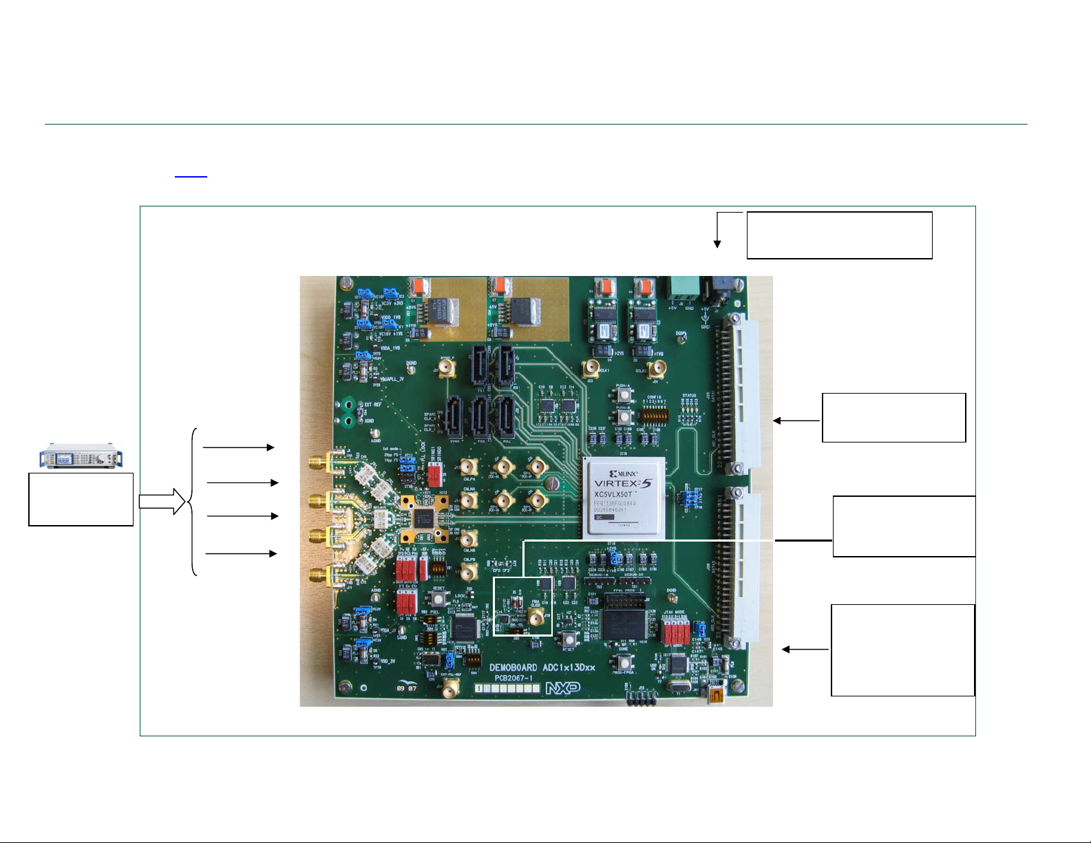
1.2 Essential Features of the Demonstration Board
Fig. 2 shows the ADC1413D125 in its environment. The output is a series CML connection capable
of delivering a throughput rate of 3.125Gsps as specified by the JESD204A standard.
The input is connected through an SMA connector and 2 transformers to adapt the impedance and
create a differential input to the ADC
The logic device Field Programmable Gate Array (FPGA) is connected to the ADC1413D125D via
2 Lanes with each lane in differential CML referenced to the positive supply. Moreover a
synchronization signal, SYNC, is routed in differential also, between the FPGA and the
ADC1413D125D.
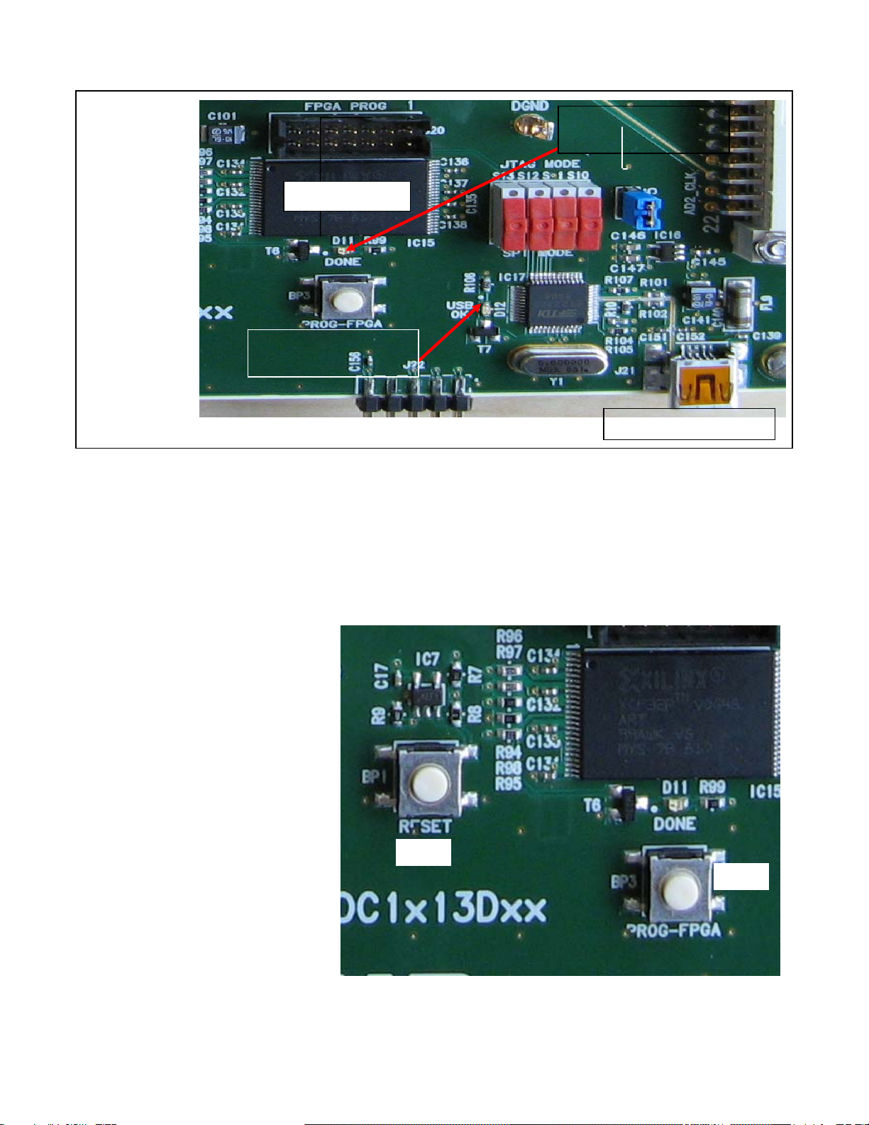
The board contains also a flash memory as shown in Fig. 4, to store the configuration file of the
FPGA. This flash memory is loaded automatically into the logic device at start up. After the bit-stream
has downloaded into the FPGA, the diode D11 lights up indicating that everything has went well.
Fig 2.ADC1413D125 with 2 lanes in pairs of CML compliant differential
Fig 3. FPGA Logic device connected to the ADC1413D125D via 2 Lanes and SYNC

Furthermore, after connecting the USB port and installing the driver, the LED D12 indicates that the
USB host has been detected and is up and running.
Flash Memory
D11 lights up: FPGA has
up-loaded its bit-stream
Fig 4. On board memory with LED D11 indicating FPGA up-loaded and running and D12 indicating USB host
detected
D12 lights up: USB Host
detected
Push Button BP1 is a manual
reset of the FPGA.
Push Button BP3 is a manual
upload of the FPGA contents
from the flash memory
Fig 5. BP1 (Manual Reset) and BP3 (Manual
upload of the flash content into the FPGA)
BP
3
BP1
Mini USB connector

Fig 6. shows the LEDs D9-D16 which are used to indicate the status of the FPGA.
The SYNC signal is a synchronization signal used at the beginning of the transmission. It is always
present between the FPGA and the ADC until the data is transferred from the ADC1413D125 to
the logic device . It is also used by the receiver to trigger loss of synchronization and requests re-
initialization.
The clock signal can be generated on the board as there is a Phase Locked Loop (PLL) available.
However for performance assessment we recommend to use an external clock for the FPGA and
theADC DAC. This clock should come from a unique clock generator and is known as the FRAME
clock. It is the timing reference of the circuit.
D13 FPGA clk heart beat
D14 Sync signal is active
D15 K28.5 received
D16 14 bits Data are reverted
8bits by 8 bits
PUSH-A Perform a Manual Synchronization between
FPGA and ADC
PUSH-B Invert 14 bits parallel data Byte wise ( 8 bits by
8 bits)
Fig 6. D13 – D16 indicates the status of the FPGA

Remark: as the clock can come either internally or externally, multiplexers are available so as to
route the right clock signal to the devices, the ADC1413D125 and the FPGA.
When using an external clock the double switch SW5 should be set to the “ON” position.
Fig 7. Clock Inputs
Clock signal
coming from
one generator
and fed to J19
and CLKP
Clock Generator
-PLL
-CML/LVDS
-Direct input
available

2. Example
2.1 Setup example
Fig 9. ADC1413D125D Demonstrator Hardware set
SMA 100 A
Rohde & Schwarz
Signal Generator
USB SPI
A
DC1413D125.
Register
programming
Data Acquisition
and processing1
DC adaptor
connected to mains
SMA 100 A
Rohde & Schwarz
Clock Generator

3. SPI quick start
3.1 Install
The demonstration board is delivered with the following software:
Labview Runtime: LabVIEW85RuntimeEngineFull.exe
Labview executable: Andromeda.exe
Appropriate drivers
•Step 1
Connect the device to a USB port on your PC. Windows ‘Found New Hardware Wizard’ will be launched.
Select ‘No, not this time’ from the options available and then click ‘Next’ to proceed with the installation.

•Step 2
Select ‘Install from a list or specific location (Advanced)’ as shown below and then click ‘Next’.
•Step 3
Select ‘Search for the best driver in these locations’ and enter the file path of the folder
CD-ROM CONTENT\CD-ROM2_ADC1213d_ADC1413d_DAC1408d\Version_1.0\Driver USB \driver_d2xx’
in the combo-box (‘C:\driver_2xx’ in the example below) or browse to it by clicking the browse button. Once the
file path has been entered in the box, click ‘next’ to proceed.

•Step 4
Windows should then display a message indicating that the installation was successful. Click ‘Finish’ to
complete the installation for the first port of the device.

3.2 SPI interface
•Step 1
Install the LabVIEW Run-time Engine LabVIEW85RuntimeEngineFull.exe (if not already installed).
•Step 2
Start the LabVIEW application “ADC1x13.exe”. a graphical window will pop-up
Under the “ Write register from command file” field, choose the write configuration file from “ADC Command”
directory depending on the used operating points.
Click on the “read from config file”.
Push the Push_A button on the board to make a manual synchronization of the JESD204A communication.
Fill the Input Frequency and Clock Frequency fields with the wanted operating points.

Click on ADC button to choose between internal ADC capture or FPGA capture
Click on Load DATA to get the FFT and the ADC performances

Select
Input Frequency = 150M
A
DC clock = 76.8M
Check input level here
« latest MRA » button must
be
g
reen
Select « use coherence » when
clock input coherence is OK in
order to get SFDR value
calculation
Select SPI setting file then
click “read config from file” in
order to write SPI setting in the
device.
SNR value (dbFS)
SFDR value (dBFS)
Valid only with single tone
si
g
nal
Displa
y
Zoom selection
Select the wanted ADC
in
p
ut channel.
Select FFT without window
(
Clock coherenc
y
OK
)
Load Data to start
capturing
Table of contents
Other Conrad Motherboard manuals