3 PCB Layout Guideline
4 Bill of Materials, Board Layout, and Schematic
4.1 Bill of Materials
PCB Layout Guideline
www.ti.com
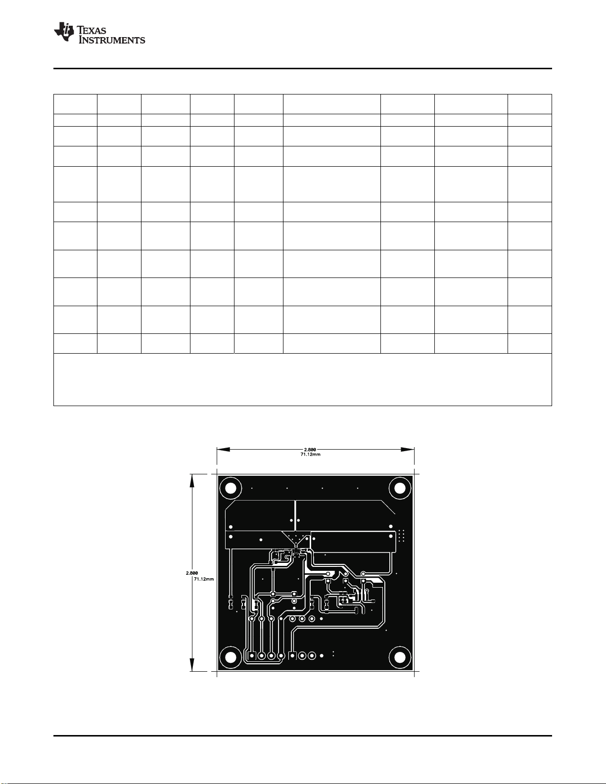
1. It is critical that the exposed power pad on the backside of the bq2435x package be soldered to theprinted-circuit board (PCB) ground. Ensure that sufficient thermal vias are located underneath the IC,connecting to the ground plane on the other layers.2. The high-current charge paths into ACIN and from CHGIN, OUT pins must be sized appropriately forthe maximum charge current in order to avoid voltage drops in these traces.3. Decoupling capacitors for ACIN, CHGIN must be placed and make the interconnections to the IC asshort as possible.4. Resistors for VBAT pin must be placed close to the corresponding IC pins and make theinterconnections to the IC as short as possible.
Table 1. Bill of Materialsbq24350 bq24352 - bq24355 - RefDes Value Description Size Part Number MFR-001 002 003
1 1 1 C1 1uF Capacitor, Ceramic, 35V, 603 Std StdX5R, 10%
3 3 3 C2, C3, C5 1uF Capacitor, Ceramic, 10V, 603 Std StdX7R, 10%
1 1 1 C4 0.1uF Capacitor, Ceramic, 16V, 805 Std StdX7R, 10%
1 1 1 C6 0.1uF Capacitor, Ceramic, 10V, 603 Std StdX7R, 10%
1 1 1 C7 220uF Capacitor, Electrolytic, 25V, 0.327 X 0.327 UUD1E221MNL1GS Nichicon20% inch
1 1 1 D1 BZT52C6V8S Diode, Zener, 200mW, 6.8V SOD-323 BZT52C6V8S General
3 3 3 D2, D3, D6 Green Diode, LED, Green, 2.1-V, 603 LTST-C190GKT Lite On20-mA, 6-mcd
2 2 2 D4, D7 Red Diode, LED, Red, 2.1-V, 603 LTST-C190CKT Lite On20-mA, 6-mcd
1 1 1 D5 BAT54C Diode, Dual Schottky, SOT23 BAT54C Vishay-200-mA, 30-V Liteon
2 2 2 J1, J4 ED1514/2DS Terminal Block, 2-pin, 6-A, 0.27 x 0.25 ED1514/2DS OST3.5mm inch
2 2 2 J2, J3 ED1516/4DS Terminal Block, 4-pin, 6-A, 0.55 x 0.25 ED1516/4DS OST3.5mm inch
5 5 5 JP1, JP4, PEC02SAAN Header, 2-pin, 100mil 0.100 inch x 2 PEC02SAAN SullinsJP5, JP6, spacingJP7
2 2 2 JP2, JP3 PTC03SAAN Header, Male 3-pin, 100mil 0.100 inch x 3 PTC03SAAN Sullinsspacing, (36-pin strip)
5 5 5 JP1, JP2, 929950-00 Shorting jumpers, 2-pin, 929950-00 3M/ESDJP4, JP5, 100mil spacing,JP6
2 2 0 R1, R2 0 Resistor, Chip, 1/16W, 1% 402 Std Std
0 0 2 R3, R4 0 Resistor, Chip, 1/16W, 1% 402 Std Std
2 2 2 R5, R6 200k Resistor, Chip, 1/16W, 5% 402 Std Std
2 2 2 R7, R8 200k Resistor, Chip, 1/16-W, 5% 603 Std Std
2 2 2 R9, R10 0.2 Resistor, Metal Film, 1/4 watt, 1206 Std Std1%
1 1 1 R11 20k Resistor, Chip, 1/16-W, 5% 603 Std Std
1 1 1 R12 1k Resistor, Chip, 1/16-W, 5% 603 Std Std
1 1 1 R13 100 Resistor, Chip, 1/16-W, 5% 603 Std Std
1 1 1 R14 6.2k Resistor, Chip, 1/16-W, 5% 603 Std Std
4 4 4 R15, R16, 1.5k Resistor, Chip, 1/16-W, 5% 603 Std StdR17, R18
6bq2435x DSG EVM for Li-Ion Charger Front-End Protection IC SLUU365 – June 2009Submit Documentation Feedback
