Cosmo CEB-V850ES/FJ3 Instructions for use

CEB-V850ES/FJ3·SJ3 Evaluation Board HardwareUser’s Manual
CEB-V850ES/FJ3·SJ3 EVALUATION BOARD
HARDWARE USER’S MANUAL
Date Published Sep. 2007 (The 1.1 st edition)
COSMO Co., Ltd.
Control No. CCEB-HUMFJ3SJ3_01_1E

CEB-V850ES/FJ3·SJ3 Evaluation Board HardwareUser’s Manual
Cautions
•The information in this document is subject to change without notice. Before using this document,
please confirm that this is the latest version.
•No part of this document may be copied or reproduced in any form or by any means without the prior
written consent of COSMO Co., Ltd.
•COSMO Co., Ltd. does not assume any liability for infringement of patents, copyrights or other
intellectual property rights of third parties by or arising from use of device described herein or any
other liability arising from use of such device. No license, either express, implied or otherwise, is
granted under any patents, copyrights or other intellectual property rights of COSMO Co., Ltd.
Descriptions of circuits, and other related information in this document are provided for illustrative
purposes in semiconductor product operation and application examples. The incorporation of these
circuits, and information in the design of the customer’s equipment shall be done under the full
responsibility of the customer. COSMO Co., Ltd. assumes no responsibility for any losses incurred by
the customer or third parties arising from the use of these circuits, and information.
The information in this document is current as of 2007. The information is subject to change without
notice.
Trademarks
CEB-V850ES/FJ3·SJ3 is a trademark of COSMO Co., Ltd.
Other company names and product names provide in this document are either registered trademarks or
trademarks of respective companies.

CEB-V850ES/FJ3·SJ3 Evaluation Board HardwareUser’s Manual
CONTENTS
1. Overview .....................................................................................................................................................1
2. Document....................................................................................................................................................1
3. Hardware Specifications..............................................................................................................................2
3.1 Overview .....................................................................................................................................................2
3.2 Block Diagram.............................................................................................................................................3
3.3 Configuration...............................................................................................................................................4
3.3.1 Power supply........................................................................................................................................5
3.3.2 CAN-I/F................................................................................................................................................7
3.3.3 LIN-I/F................................................................................................................................................ 11
3.3.4 Expansion connectors (J5, J6)...........................................................................................................14
3.3.5 7-segment LED (LED1)......................................................................................................................15
3.3.6 8-bit DIP SW (SW1) ...........................................................................................................................15
3.3.7 RESET...............................................................................................................................................16
3.3.8 INTP0 SW (SW2)...............................................................................................................................17
3.3.9 NMI SW (SW3)...................................................................................................................................17
3.3.10 CLOCK...............................................................................................................................................18
3.3.11 USB....................................................................................................................................................19
3.3.12 Evaluation environment......................................................................................................................21
3.3.13 The connector for MINICUBE (CN6)..................................................................................................24
3.3.14 The connector for FL-PR4, FL-PR5, MINICUBE2 (CN5)....................................................................25
3.3.15 The connector for CPU I/O pins check...............................................................................................26
3.4 Memory map .............................................................................................................................................28
3.5 Notes at the time of user circuitry..............................................................................................................30
3.5.1 Consumption current..........................................................................................................................30
3.5.2 I/O signals..........................................................................................................................................30
3.6 A jumper setup at the time of shipment .....................................................................................................31
4. CAN expansion board ...............................................................................................................................32
4.1 Specifications.....................................................................................................................................32
4.2 Block diagram ....................................................................................................................................32
4.3 Board size..........................................................................................................................................33
4.4 External connectors............................................................................................................................34
4.5 Evaluation board mating.....................................................................................................................35

1
1. Overview
This manual prescribes a CEB-V850ES/FJ3 Evaluation Board and a CEB-V850ES/SJ3 Evaluation Board.
The CEB-V850ES/FJ3 features an NEC Electronics-made 32-bit single-chip microcontroller V850ES/FJ3.
The CEB-V850ES/SJ3 features an NEC Electronics-made 32-bit single-chip microcontroller V850ES/SJ3.
In addition, USB interface, 7-segment LED, CAN interface, LIN interface, N-wire connector, etc. are carried
as a common device.
Moreover, the CEB-V850ES/FJ3 Evaluation Board can extend a CAN port by two channels by connecting
an optional CAN expansion board(CAN-EXT BOARD).
The MINICUBE or the MINICUBE2 by NEC electronics incorporated company can be used as development
environment.
The FL-PR4 or the FL-PR5 (or the FP-LITE) made by Naito Densei Machida Mfg. Co., Ltd. are required for
writing programs.
*The MINICUBE, the MINICUBE2, the FL-PR4, and the FL-PR5 are not included with this evaluation kit.
2. Document
The following documents are included as PDF files.
CEB-V850ES/FJ3·SJ3 Evaluation Board Hardware User's Manual
CEB-V850ES/FJ3 Evaluation Board Circuit Diagrams
CEB-V850ES/FJ3 Evaluation Board Parts List
CEB-V850ES/SJ3 Evaluation Board Circuit Diagrams
CEB-V850ES/SJ3 Evaluation Board Parts List
V850ES/FJ3 Hardware Preliminary User's Manual
V850ES/SJ3 Hardware Preliminary User's Manual
In addition, please refer to attached "document list."

CEB-V850ES/FJ3·SJ3 Evaluation Board HardwareUser’s Manual
2
3. Hardware Specifications
3.1 Overview
The specifications of the CEB-V850ES/FJ3·SJ3 Evaluation Board are shown below.
•CPU V850ES/FJ3 × 1 (or V850ES/SJ3)
·V850ES/FJ3
Operating CLK direct mode: 6 MHz, PLL mode: 48 MHz
Oscillator (MAIN: 6 MHz , SUB: 32.768 KHz )
·V850ES/SJ3
Operating CLK direct mode: 4 MHz, PLL mode: 32 MHz
Oscillator (MAIN: 4 MHz , SUB: 32.768 KHz )
* The crystal for MAIN clocks is socket-mounted.
•Check pin A through hole for each signal line check is around CPU.
( Two rows of half pitch)
•External connectors Expansion connector (30-pin 2.54 pitch) × 2
Connector for FL-PR4, FL-PR5, MINCUBE2 (16-pin) × 1
MINICUBE connector (26-pin) × 1
CAN-I/F connector (D-SUB 9-pin [female] ) × 2
LIN-I/F connector (3-pin) × 2
•SW PUSH SW × 3 (RESET, NMI, INTP0 )
DIP SW (8-bit) × 1
•Jumpers Development environment setting
(MINICUBE2 / MINICUBE, FL-PR4, FL-PR5)
UART setting
(USB / FL-PR4, FL-PR5, MINICUBE2)
CAN termination resistance setting
LIN-master/slave switching
•LED Power LED (+5 V ): Green,
7-segment LED × 1
•Check pin +12 V, +5 V, +3.3 V, GND
•Power supply AC adapter (DC+12 V) input
With regulator IC, +5 V(FJ3) , +3.3V(SJ3) output

CEB-V850ES/FJ3·SJ3 Evaluation Board HardwareUser’s Manual
3
3.2 Block Diagram
Whole block diagram
FJ3
MINICUBE
FL-PR4/FL-PR5/MINICUBE2
LIN0 LIN1CAN0 CAN1
DRV
DRV
DRV
DRV
ExpansionJ5 Expansion J6
C_POW
C_POW
+12V
RESET NMI INTP0
DIPSW 8 bit 7seg 8bit
Power supply
+12V IN
5/3.3
reg
C-POW
USB
miniB
VBUS
+5V
RFJ
RSJ
Max 500mA
12 / 5
reg
+12 V
USB
USB/
UART
V850ES/FJ3 Evaluation Board whole block diagram
Figure 3.2
The above figure is the case where V850ES/FJ3 is mounted. In this case, CPU power supply voltage is set
to +5V. Moreover, when V850ES/SJ3 is mounted, CPU power supply voltage is set to +3.3V.*
* Since a voltage setup is set up at the time of shipment, especially a visitor does not need to be conscious
of it.

CEB-V850ES/FJ3·SJ3 Evaluation Board HardwareUser’s Manual
4
3.3 Configuration
The following figure shows the physical placement and the outside of the major components on the
CEB-V850ES/FJ3·SJ3 evaluation CPU board.
The various components are described below.
Figure 3.3
CN1:CAN0(FJ3) CAN1(SJ3), CN2:CAN1(FJ3) CAN0(SJ3), CN3:LIN0, CN4:LIN1
CN5:FL-PR4 / FL-PR5 / MINICUBE2, CN6:MINICUBE
CN7:USB
CN8:POWER
J5:EXPANSION, J6:EXPANSION
SW1:DIP8bit, SW2:INTP0, SW3:NMI, SW4:RESET
CN1
CN2
CN3 CN4
CN7
J5
J6 SW1
SW2
SW3
SW4
CN1
CN2
CN3 CN4
CN5
CN6
CN7
CN8
J5
J6 SW1
SW2
SW3
SW4
CEB-V850ES/FJ3·SJ3 Evaluation Board HardwareUser’s Manual
5
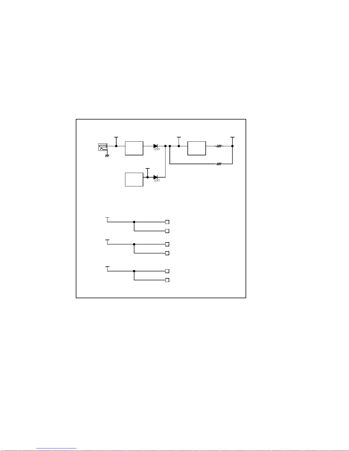
3.3.1Power supply
(1) Power supply part
Although premised fundamental on use in +12V input from the attached AC/DC adaptor, it is possible to
also make it operate by the power supply supply from a USB port.
Notes: As for the USB port, power supply supply capability is restricted to 500mA by specification. When
you operate this board in a USB port, please use consumption current by 500mA or less. moreover, since
+5V are supplied from a USB port, A LIN-I/F function cannot be used.
A block diagram is shown below.
Power Supply
+12 V IN 5/3.3
reg
C-POW
USB
miniB
VBUS
+5 V
RFJ
RSJ
Max500 mA
12 / 5
reg
+12V
+12V LIN-0
LIN-1
Peripheral IO device
Expansion connectors
+5V
C-POW CPU
CPU Peripheral
(Pull -up resistance )
Figure 3.3.1(1)

CEB-V850ES/FJ3·SJ3 Evaluation Board HardwareUser’s Manual
6
(2) Power supply connector (CN8)
Please use DC jack side of an attached AC adaptor for a power supply connector (CN8), connecting.
The power supply to supply is as follows.
AC adaptor : NP12-US1210 (Akizuki Denshi Corp)
Input voltage range : AC100-240 V 50/60 Hz
Output voltage : DC12 V
Current : 1 A max
Suitable connector : Type A (φ5.5)
Polarity :
GND
GND
+12V+12V
Figure 3.3.1 (2)

CEB-V850ES/FJ3·SJ3 Evaluation Board HardwareUser’s Manual
7
3.3.2CAN-I/F
(1) CAN-I/F overview
Two CAN interfaces are mounted as standard.
A block diagram is shown below.
CTXDn TXD
RXD
CAN_H
CAN_L
CAN transceiver
( TJA 1050 )
1
6
2
7
3
8
4
9
5
RS
CRXDn
V850ES/FJ3·SJ3
Common
mode filter
Terminator
change jumper
JP1,2
Open setting
jumper
JPX2,4
D-SUB
9 pin
[ female]
P***
Open setting
jumper
JPX1,3
Figure 3.3.2(1)

CEB-V850ES/FJ3·SJ3 Evaluation Board HardwareUser’s Manual
8
(2) CAN-I/F connector (CN1, CN2)
In the case of CEB-V850 ES/FJ3, CAN0 is assigned to CN1 and CAN1 is assigned to CN2, respectively.
In the case of CEB-V850 ES/SJ3, CAN1 is assigned to CN1 and CAN0 is assigned to CN2, respectively.
Since the connector on a substrate mounts Dsub9 pin (female), the connector by the side of a cable should
use Dsub9 pin (male) at the time of cable creation.
Pin distribution table is shown below.
CAN I/F connector pin distribution table
Pin№CN1(CAN0:FJ3 CAN1:SJ3) CN2(CAN1:FJ3 CAN0:SJ3)
1 N.C. N.C.
2 CAN_L0(FJ3) CAN_L1(SJ3) CAN_L1(FJ3) CAN_L0(SJ3)
3 GND GND
4 N.C. N.C.
5 Coupling with capacitor and fed to GND. Coupling with capacitor and fed to GND.
6 N.C. N.C.
7 CAN_H0(FJ3) CAN_H1(SJ3) CAN_H1(FJ3) CAN_H0(SJ3)
8 N.C. N.C.
9 N.C. N.C.
Table 3.3.2 (2)
Loading connector part number : XM3B-0922-112 (OMRON Corp.)

CEB-V850ES/FJ3·SJ3 Evaluation Board HardwareUser’s Manual
9
(3) CAN transceiver
TJA1050T (Philips Corp.) are mounted in this board as a CAN transceiver.
Refer to the applicable data sheet for the details of a device.
Connection of CPU and a CAN transceiver is shown below.
CN1 connection
CPU TJA1050T Signal Name
CTXD0(FJ3) CTXD1(SJ3)(P33)TXD Transmitting data
CRXD0(FJ3) CRXD1(SJ3)(P34)RXD Receiving data
VREF VREF
CAN_H,CAN_L CAN
PCM4 RS RS
VCC,GND
Power supply(+5Vsupply)
Table 3.3.2 (3)-1
CN2 connection
CPU TJA1050T Signal Name
CTXD1(FJ3) CTXD0(SJ3)(P36)TXD Transmitting data
CRXD1(FJ3) CRXD0(SJ3)(P37)RXD Receiving data
VREF VREF
CAN_H,CAN_L CAN
PCM5 RS RS
VCC,GND Power supply(+5Vsupply)
Table 3.3.2 (3)-2
(4) CAN signal terminus setup
A CAN signal terminus value is set up by JP1 and JP2.
JP1 corresponds to CN1 and JP2 correspond to CN2, respectively.
Setup Terminator value (common to JP1 and JP2)
Open Infinite (default)
1-2 short circuit 120Ω
1-2,3-4 short circuit 60Ω
Others Prohibition of a setup
Table 3.3.2 (4)
JP1,2
4 2
3 1

CEB-V850ES/FJ3·SJ3 Evaluation Board HardwareUser’s Manual
10
(5) About JPX1-JPX4
Although the pattern connects between 1-2 and between 3-4 of JPX1-JPX4, a signal is separable by cutting
the pattern on the back side (soldering side) of each jumper.
As standard, the following jumper is un-mounting.
The installation part of each jumper is shown below.
JPX Function
JPX1 CN1 ( Between CAN transceiver - CAN connector )
JPX2 CN1 ( Between CPU - CAN transceiver )
JPX3 CN2 ( Between CAN transceiver - CAN connector )
JPX4 CN2 ( Between CPU - CAN transceiver )
Table 3.3.2 (5)
JPX1,3
4 2
3 1
JPX2,4
4 2
3 1
CEB-V850ES/FJ3·SJ3 Evaluation Board HardwareUser’s Manual
11
3.3.3LIN-I/F
(1) LIN-I/F outlline
Two LIN interfaces are mounted as standard.
A block diagram is shown below.
TXDA* TXD
RXD
LIN
LIN transceiver
(TJA1020)
NSLP
+12V
RXDA*
V850ES/FJ3·SJ3
Open setting
jumper
JPX5 , 8
3pin
connector
P***
BAT
1
2
3
Open setting
jumper
JPX6 , 10
Open setting
jumper
JPX7 , 9
NWAKE
INH Master / Slave
Change jumper
JP3 , 5
Master / Slave
Change jumper
JP4 , 6
Cmaster Cslave
+12V
Figure 3.3.3 (1)
(2) LINE-I/F connector (CN3, CN4)
LIN0 is assigned to CN3 and LIN1 is assigned to CN4, respectively.
Connector pin distribution table is shown below.
LIN I/F connector pin description
Pin№CN3(LIN0)CN4(LIN1)
1 LIN_Bus LIN_Bus
2 +12V +12V
3 GND GND
Table 3.3.3 (2)
Loading connector part number : IL-SP-S3FP2(J.S.T. Mfg Co.Ltd.)

CEB-V850ES/FJ3·SJ3 Evaluation Board HardwareUser’s Manual
12
(3) LIN transceiver
TJA1020T (Philips Corp.) are mounted in this board as a LIN transceiver.
Refer to the applicable data sheet for the details of a device.
Connection of CPU and a LIN transceiver is shown below.
LIN0
CPU TJA1020T Signal name
RXDD2(P39)RXD Reception
P63 NSLP SLEEP MODE
(pullup)NWAKE
TXDD2(P38)TXD Transmission
LIN LIN
(JP3)INH MASTER/SLAVE
BAT,GND Powersupply(+12V supply)
Table 3.3.3 (3)-1
LIN1
CPU TJA1020T Signal name
RXDD3(P80)RXD Reception
P64 NSLP SLEEP MODE
(pullup)NWAKE
TXDD3(P81)TXD Transmission
LIN LIN
(JP5)INH MASTER/SLAVE
BAT,GND Power supply(+12V supply)
Table 3.3.3 (3)-2
(4) LIN MASTER/SLAVE setting
A jumper is set up by the mode of LIN of operation.
・LIN0 MASTER/SLAVE
Jumper MASTER setting SLAVE setting
JP3 2-3 short circuit (default) 1-2 short circuit
JP4 1-2 short circuit (default) 2-3 short circuit
Table 3.3.3 (4)-1
・LIN1 MASTER/SLAVE
Jumper MASTER setting SLAVE setting
JP5 2-3 short circuit 1-2 short circuit (default)
JP6 1-2 short circuit 2-3 short circuit (default)
Table 3.3.3 (4)-2
JP3−6
1
2
3

CEB-V850ES/FJ3·SJ3 Evaluation Board HardwareUser’s Manual
13
(5) About JPX5-JPX10
Although the pattern connects between 1-2 and between 3-4 of JPX5-JPX8, and between 1-2 of JPX6,
JPX9, JPX10, a signal is separable by cutting the pattern on the back side (soldering side) of each jumper.
As standard, the following jumper is un-mounting.
The installation part of each jumper is shown below.
JPX Function
JPX5 LIN0 ( Between CPU - LIN transceiver )
JPX6 LIN0 ( Between CPU – LIN transceiver NSLP )
JPX7 LIN0 ( Between LIN transceiver – LIN connector )
JPX8 LIN1 ( Between CPU – LIN transceiver )
JPX9 LIN1 ( Between CPU – LIN transceiver NSLP )
JPX10 LIN1 ( Between LIN transceiver – LIN connector )
Table 3.3.3 (5)
4 2
JPX5,8
3 1
JPX6,7,9,10
1 2

CEB-V850ES/FJ3·SJ3 Evaluation Board HardwareUser’s Manual
14
3.3.4 Expansion connectors (J5, J6)
A signal can be pulled out from this connector and it can connect with a user circuit. Moreover, an optional
*CAN expansion board is connectable.
As standard, it is not mounted.
Expansion connectors table
J5 J6
Pin
№Signal name Function used
on a Board Pin
№Signal name Function used
on a Board
1 P00 8bit DIP-SW 1 P98/SOB1(A8) -
2 P10/INTP9 - 2 P912/_SCKB2(A12) -
3 P01 8bit DIP-SW 3 P99/_SCKB1(A9) -
4 P11/INTP10 - 4 P913/INTP4(A13) -
5 P03/INTP0 Push-SW(INTP0)5 P910/SIB2(A10) -
6 P32/ASCKA0 8bit DIP-SW 6 P914/INTP5(A14) -
7 P04/INTP1 - 7 P911/SOB2(A11) -
8 P35 8bit DIP-SW 8 P915/INTP6(A15) -
9 P06/INTP3 - 9 PCS0/_CS0 -
10 P41/SOB0 Flash PRO4 10 PCM0/_WAIT
11 P40/SIB0 Flash PRO4 11 PCS1/_CS1 -
12 P42/_SCKB0 Flash PRO4 12 P36(IETX0) -
13 P50/KR0 8bit DIP-SW 13 PCS2/_CS2 -
14 P53/KR3/DDO N-Wire 14 P37(IERX0) -
15 P51/KR1 8bit DIP-SW 15 PCS3/_CS3 -
16 P54/KR4/DCK N-Wire 16 PCT5 8bit DIP-SW
17 P52/KR2/DDI N-Wire 17 P73/ANI3 -
18 P55/KR5/DMS N-Wire 18 PCT7 8bit DIP-SW
19 P90/TXDA1(A0) - 19 P72/ANI2 -
20 P95(A5) - 20 P60/INTP11 Expansion CAN(CAN2)RS
21 P91/RXDA1(A1) - 21 P61/INTP12 Expansion CAN(CAN3)RS
22 P96(A6) - 22 P70/ANI0
23 P92(A2) - 23 P71/ANI1 -
24 P97/SIB1(A7) - 24 P65/CTXD2 Expansion CAN(CAN2)TXD
25 P93(A3) - 25 P66/CRXD2 Expansion CAN(CAN2)RXD
26 CPOW 26 +5V
27 P94(A4) - 27 P67/CTXD3 Expansion CAN(CAN3)TXD
28 _RESET Push-SW(RESET)28 P68/CRXD3 Expansion CAN(CAN3)RXD
29 GND 29
+12V -
30 GND 30
GND
Table 3.3.4
The pull-up of each signal is carried out by resistance 47kΩ.
CPOW=CPU power supply FJ3:+5V, SJ3:+3.3V
*Refer to Chapter 4.

CEB-V850ES/FJ3·SJ3 Evaluation Board HardwareUser’s Manual
15
3.3.5 7-segment LED (LED1)
The seven-segment LED is mounted on a board.
The LED can be statically switched on the light or put out from the port of CPU.
In case you make each segment turn on, please set a corresponding port as "0."
f b
e c
d
g
a
DP
a.PCD
0
b.PCD
1
c.PCD2
d.PCD
3
e.PCS4
f.PCS5
g.PCS6
DP.PCS
7
Figure 3.3.5
Segment Correspondence port Light/Extinguish default
a PCD0 0 / 1 1(pullup)
b PCD1 0 / 1 1(pullup)
c PCD2 0 / 1 1(pullup)
d PCD3 0 / 1 1(pullup)
e PCS4 0 / 1 1(pullup)
f PCS5 0 / 1 1(pullup)
g PCS6 0 / 1 1(pullup)
D.P. PCS7 0 / 1 1(pullup)
Table 3.3.5
3.3.6 8-bit DIP SW (SW1)
8-bit DIP SW is mounted on a board.
ON/OFF of DIP SW can be checked in a CPU port.
If DIP SW is turned "ON", a port will be set to "0", and a port will be set to "1" if it turns "OFF."
bit Port
DIP-SW1 P50
DIP-SW2 P51
DIP-SW3 PCT5
DIP-SW4 PCT7
DIP-SW5 P32
DIP-SW6 P35
DIP-SW7 P00
DIP-SW8 P01
Table 3.3.6

CEB-V850ES/FJ3·SJ3 Evaluation Board HardwareUser’s Manual
16
3.3.7 RESET
(1) RESET overview
When the time of power on or SW4 are pushed, reset starts a board.
It is a RESET signal at the MINICUBE or FL-PR4 or FL-PR5 use and MINICUBE2 use time, and
composition differs.
A reset signal block diagram is shown below.
MINICUBE2
/ RESin
Resistance for
logic stable
11
12
13
14
15
16
VDD2
FLMD1
RFU-1
FLMD0
(/RESin)
NC
FJ3/ SJ3 MINICUBE·FL-PR4 / FL-PR5/ MINICUBE2 connection
CN 5
FL-PR4 / FL-PR5 / MMINICUBE 2 connector
1
2
3
4
5
6
7
8
9
10
GND
/ RESout
SI/ RXD
VDD
SO/TXD
VPP
SCK
H/S
CLK
VDE
CN6
MINICUBE
A7
A8
A9
A10
A11
A12
A13
DDI
DCK
DMS
DDO
/DRST
/RESET
FLMD0 MINICUBE , FL-PR4, FL-PR5 and
MINICUBE2 are promised on
exclusion use, respectively.
(/ RESET signal is communalized)
C- POW
(Resetsignalblock diagram)
P30/ TXD0
P31/ RXD0
FLMD0
FLMD1
/RESET
DDI
DCK
DMS
DDO
/DRST
V850FJ3/SJ3
P62
C-POW
Short pin
2-3
1-2
1-2
1-2
Select
A
B
B
B
Connection apparatus
MINICUBE2
MINICUBE
FL-PR4
FL-PR5
MINICUBE2
FL- PR4, FL-PR5
MINICUBE
The flow of a reset signal
AY
BA/B
_
A
B
Y
A/B
_
C-POW
C-POW
Nothing 1- 2 B
FL-PR4/FL-PR5 /
MINICUBE 2 connector
SW4
JP7
Figure 3.3.7(1)

CEB-V850ES/FJ3·SJ3 Evaluation Board HardwareUser’s Manual
17
(2)RESET signal setting (JP7)
A setup of a RESET signal changes with apparatus connected.
JP7 performs a setup.
JP7 Function
1-2 short circuit Normal use, During connecting FL-PR4, FL-PR5, MINICUBE (Default )
2-3 short circuit During connecting MINICUBE2
Table 3.3.7 (2)
In case FL-PR4 or FL-PR5 or MINICUBE are used, a JP7 short pin is set to the "1-2" side, and it is set as
the course of dashed-and-dotted line (FL-PR4) and a dotted line (MINICUBE) among Figure 3.3.7(1).
(Refer to reset signal block diagram)
In case MINICUBE2 is used, a JP7 short pin is set to the "2-3" side, and it is set as the course of a solid
line (MINICUBE2) among Figure 3.3.7(1).
Please use a JP7 short pin for the "1-2" side at the time of real operation, setting it up (when you do not use
a debugger).
(3)RESET SW (SW4)
If SW4 is pushed, CPU and an evaluation board will be in a reset state.
3.3.8 INTP0 SW (SW2)
SW2 on a board is connected to P03-/INTP0 port.
A push on SW2 inputs "0" into P03-/INTP0 port.
3.3.9 NMI SW (SW3)
SW3 on a board is connected to P02-/NMI port.
A push on SW3 inputs "0" into P02-NMI port.
JP7
1
2
3
This manual suits for next models
1
Table of contents


