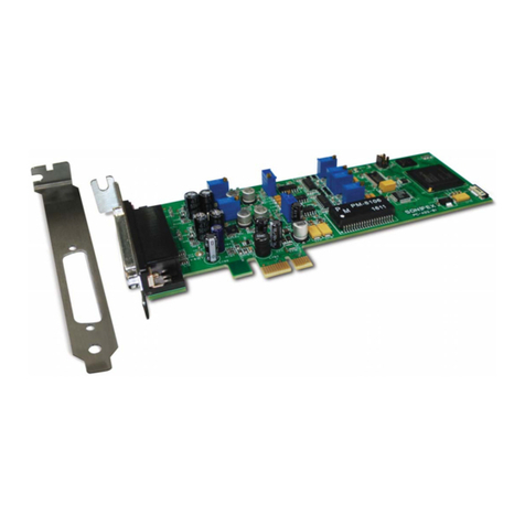
Crystal CS4281 Owner's manual

Revision 1.17w
1
Copyright Cirrus Logic, Inc. 2000
(All Rights Reserved)
P.O. Box 17847, Austin, Texas 78760
(512) 445 7222 FAX: (512) 445 7581
http://www.cirrus.com
CS4281
Programming Manual
3/7/00
Confidential Draft3/7/00
MAR’00
DS308PRM1
Draft

Confidential Draft 3/7/00
CS4281 Programming Manual
2DS308PRM1
Contacting Cirrus Logic Support
For a complete listing of Direct Sales, Distributor, and Sales Representative contacts, visit the Cirrus Logic web site at:
http://www.cirrus.com/corporate/contacts/
Preliminary product information describes products which are in production, but for which full characterization data is not yet available.
Advance product information describes products which are in development and subject to development changes. Cirrus Logic, Inc.
has made best efforts to ensure that the information contained in this document is accurate and reliable. However, the information is
subject to change without notice and is provided “AS IS” without warranty of any kind (express or implied). No responsibility is as-
sumed by Cirrus Logic, Inc. for the use of this information, nor for infringements of patents or other rights of third parties. This docu-
ment is the property of Cirrus Logic, Inc. and implies no license under patents, copyrights, trademarks, or trade secrets. No part of
this publication may be copied, reproduced, stored in a retrieval system, or transmitted, in any form or by any means (electronic, me-
chanical, photographic, or otherwise) without the prior written consent of Cirrus Logic, Inc. Items from any Cirrus Logic website or
disk may be printed for use by the user. However, no part of the printout or electronic files may be copied, reproduced, stored in a
retrieval system, or transmitted, in any form or by any means (electronic, mechanical, photographic, or otherwise) without the prior
written consent of Cirrus Logic, Inc.Furthermore, no part of this publication may be used as a basis for manufacture or sale of any
items without the prior written consent of Cirrus Logic,Inc. The names of products ofCirrus Logic, Inc. or other vendors and suppliers
appearing in this document may be trademarks or service marks of their respective owners which may be registered in some jurisdic-
tions. A list of Cirrus Logic, Inc. trademarks and service marks can be found at http://www.cirrus.com.
Draft

CS4281 Programming Manual
DS308PRM1 3
Confidential Draft
3/7/00
TABLE OF CONTENTS
1. DEFINITION OF TERMS ........................................................................................................13
2. INTRODUCTION ..................................................................................................................... 15
2.1 Typical System Diagrams ................................................................................................ 17
2.1.1 Surround Sound 5.1 Play .................................................................................... 19
2.2 Audio Data Flow Diagrams .............................................................................................. 20
2.3 AC ‘97 Configurations ...................................................................................................... 22
3. GENERAL OVERVIEW .......................................................................................................... 25
3.1 Functional Specs ............................................................................................................. 25
3.2 General Specs ................................................................................................................. 25
3.3 Digital Filter Specs ........................................................................................................... 33
3.4 Implied Functional Specs ................................................................................................ 33
4. PINOUT ................................................................................................................................... 35
4.1 Physical Pin Placement - CS4610/14/CS4280 Compatible 100 Pin MQFP .................... 35
4.2 Physical Pin Placement - 100 Pin TQFP ......................................................................... 36
4.3 Pin Descriptions ............................................................................................................... 37
4.3.1 PCI Interface ....................................................................................................... 37
4.3.2 Clock/Miscellaneous ........................................................................................... 39
4.3.3 External Interface Pins ........................................................................................ 40
4.3.4 Clock/Miscellaneous ........................................................................................... 41
4.3.5 Serial Codec Interface ........................................................................................ 42
5. PCI PROPERTIES AND CONFIGURATION .......................................................................... 45
5.1 Slave Interface Properties ............................................................................................... 45
5.1.1 Supported Cycles ................................................................................................ 45
5.1.2 Unsupported Cycles ............................................................................................ 45
5.1.3 Error Conditions .................................................................................................. 45
5.1.4 Protocol Support ................................................................................................. 45
5.2 Master Interface Properties ............................................................................................. 46
5.2.1 Generated Cycles ............................................................................................... 46
5.2.2 Cycles Not Generated ......................................................................................... 46
5.3 Configuration Space ........................................................................................................47
5.3.1 Configuration Write Protect Register (CWPR) .................................................... 49
5.4 Subsystem ID and Vendor ID Field Initialization ............................................................. 50
5.4.1 Subsystem Vendor ID/Subsystem ID Pre-load Register (SSVID) ...................... 50
6. PCI INTERFACE ..................................................................................................................... 51
7. HOST-INTERFACE PROGRAMMING MODEL ..................................................................... 51
7.1 BA0 Register Map ...........................................................................................................52
7.2 BA1 Direct Memory Map ................................................................................................ 55
7.3 Config Space Map ...........................................................................................................56
8. START-UP CONFIGURATION AND STATUS ...................................................................... 57
8.1 PCI Start-Up Configuration .............................................................................................. 57
8.2 Sound System Start-Up Configuration ............................................................................ 58
8.2.1 Sound System Playback ..................................................................................... 59
8.2.2 Sound System Record ........................................................................................ 59
8.2.3 6-Channel Dual-Codec Playback Setup Example .............................................. 60
8.3 Feature and Configuration Reporting .............................................................................. 62
8.3.1 Feature Reporting Register (FRR) ..................................................................... 62
8.3.2 Configuration Load Register (CFLR) ................................................................. 62
9. PCI POWER MANAGEMENT ................................................................................................ 63
9.1 Power Management States ............................................................................................. 63
9.2 Modem Wakeup .............................................................................................................. 65
9.3 Register Interface ............................................................................................................ 66
9.3.1 PCI Status (PCIS) ............................................................................................... 66
Draft

Confidential Draft
3/7/00 CS4281 Programming Manual
4DS308PRM1
9.3.2 Capabilities Pointer ............................................................................................. 67
9.3.3 Capabilities ID ..................................................................................................... 67
9.3.4 Next Item Pointer ................................................................................................ 67
9.3.5 Power Management Capabilities (PMC) ............................................................. 68
9.3.6 PCI-PCI Bridge Support Extensions ................................................................... 70
9.3.7 Power Data ......................................................................................................... 70
9.3.8 Extended PCI Power Management Control (EPPMC) ........................................ 71
9.4 PME# Assertion ............................................................................................................... 73
9.5 Vaux Powered Circuitry ................................................................................................... 74
9.6 Block-Level Power-down and Reset States .................................................................... 74
9.6.1 PCI Bus Interface Unit (BIU) Block ..................................................................... 75
9.6.2 Control Block ....................................................................................................... 75
9.6.3 VAUX Block ........................................................................................................ 75
9.6.4 Sound System/DLL Block ................................................................................... 75
9.6.5 SRC Block ........................................................................................................... 75
9.6.6 Joystick Block ..................................................................................................... 75
9.6.7 MIDI Block ........................................................................................................... 76
9.6.8 Hardware Volume Block ..................................................................................... 76
9.6.9 AC-Link Engine Block ......................................................................................... 76
9.6.10 DMA/Registers Block ........................................................................................ 76
9.6.11 EEPROM Block ................................................................................................. 76
9.6.12 FM Block ........................................................................................................... 76
10. INTERRUPT SUBSYSTEM .................................................................................................. 77
10.1 PCI Interrupt Line Control .............................................................................................. 77
10.2 DMA and Polled FIFO Interrupts ................................................................................... 77
10.3 Extended GPIO and Hardware Volume Control Interrupts ............................................ 79
10.4 Interrupt Reporting Registers ........................................................................................ 80
10.4.1 Host Interrupt Status Register (HISR) ............................................................... 80
10.4.2 Host Interrupt Control Register (HICR) ............................................................. 81
10.4.3 Host Interrupt Mask Register (HIMR) ................................................................ 82
10.4.4 ISA Interrupt Enable Register (IIER) ................................................................. 83
10.4.5 ISA Interrupt Select Register (IISR) .................................................................. 84
11. DMA CONTROLLER ............................................................................................................85
11.1 System Operation ..........................................................................................................85
11.1.1 Host Interrupts for DMA Mode .......................................................................... 86
11.1.2 Host Interrupts in FIFO Polling Mode ................................................................ 86
11.2 Data Format Conversions .............................................................................................. 87
11.3 Differences from the 8237 ............................................................................................. 96
11.4 DMA Control Register Operation ................................................................................... 96
11.5 DMA Control Registers .................................................................................................. 97
11.5.1 DMA Base Address n (DBAn) ........................................................................... 97
11.5.2 DMA Current Address n (DCAn) ....................................................................... 98
11.5.3 DMA Base Count n (DBCn) .............................................................................. 99
11.5.4 DMA Current Count n (DCCn) ........................................................................ 100
11.5.5 DMA Mode Register n (DMRn) ....................................................................... 101
11.5.6 DMA Command Register n (DCRn) ................................................................ 103
11.5.7 Host DMA Status Register n (HDSRn) ........................................................... 104
11.5.8 FIFO Control Register n (FCRn) ..................................................................... 105
11.5.9 FIFO Status and Interrupt Control Register n (FSICn) .................................... 106
11.5.10 FIFO Polled Data Register n (FPDRn) .......................................................... 107
11.5.11 FIFO Channel Status (FCHS) ....................................................................... 108
11.6 FIFO Hardware Implementation .................................................................................. 110
11.6.1 Using FM/Wavetable Digital Stream from Host .............................................. 113
12. DIRECT PCI TRANSACTION GENERATION .................................................................... 115
Draft

CS4281 Programming Manual
DS308PRM1 5
Confidential Draft
3/7/00
13. PCI I/O TRAPPING ............................................................................................................. 115
13.1 Typical I/O Trap Ranges .............................................................................................. 115
13.2 Trap Actions ................................................................................................................ 116
13.3 I/O Trapping Registers ................................................................................................ 116
13.3.1 I/O Trap Game Port (IOTGP) .......................................................................... 117
13.3.2 I/O Trap - Sound Blaster (IOTSB) ................................................................... 118
13.3.3 I/O Trap - FM Synthesis (IOTFM) ................................................................... 119
13.3.4 I/O Trap - DMA (IOTDMA) .............................................................................. 120
13.3.5 I/O Trap - PCPCI (IOTPCP) ............................................................................ 121
13.3.6 I/O Trap CCLS Control Register (IOTCC) ....................................................... 122
13.3.7 I/O Trap Control Register (IOTCR) ................................................................. 124
13.4 Interface to CCLS ........................................................................................................ 125
13.4.1 CCLS Unsupported Legacy DMA Registers ................................................... 128
13.5 Interface to PC/PCI ...................................................................................................... 129
13.6 Interface to DDMA ....................................................................................................... 130
14. PC/PCI ................................................................................................................................ 131
14.1 Register Interface ........................................................................................................135
14.1.1 PC/PCI Request Register (PCPRR) ............................................................... 135
14.1.2 PC/PCI Grant Register (PCPGR) ................................................................... 136
14.1.3 PC/PCI Control Register (PCPCR) ................................................................. 136
15. DDMA ................................................................................................................................. 137
16. SOUND BLASTER .............................................................................................................139
16.1 Sound Blaster Register Addressing ............................................................................. 139
16.2 Sound Blaster Register Description ............................................................................. 140
16.2.1 Sound Blaster Mixer Address Register (SBMAR) ........................................... 140
16.2.2 Sound Blaster Mixer Data Register (SBMDR) ................................................ 141
16.2.3 Sound Blaster Reset Register (SBRR) ........................................................... 141
16.2.4 Sound Blaster Read Data Port (SBRDP) ........................................................ 142
16.2.5 Sound Blaster Write Data Port (SBWDP) ....................................................... 142
16.2.6 Sound Blaster Write Buffer Status (SBWBS) .................................................. 143
16.2.7 Sound Blaster Read Buffer Status (SBRBS) .................................................. 143
16.3 Sound Blaster Hardware Overview ............................................................................. 144
16.4 Sound Blaster Mixer .................................................................................................... 144
16.4.1 Sound Blaster Mixer Mapping onto the AC ‘97/CS4281 Mixer ....................... 144
16.5 SB Configuration Setup Requirements ........................................................................ 147
16.6 Sound Blaster DSP ...................................................................................................... 149
16.7 Sound Blaster Hardware Handshake .......................................................................... 149
16.8 Sound Blaster Reset .................................................................................................... 149
16.9 Sound Blaster Interrupts .............................................................................................. 149
17. SOUND BLASTER .............................................................................................................153
17.1 Sound Blaster Register Addressing ............................................................................. 153
17.2 Sound Blaster Register Description ............................................................................. 154
17.2.1 Sound Blaster Mixer Address Register (SBMAR) ........................................... 154
17.2.2 Sound Blaster Mixer Data Register (SBMDR) ................................................ 154
17.2.3 Sound Blaster Reset Register (SBRR) ........................................................... 155
17.2.4 Sound Blaster Read Data Port (SBRDP) ........................................................ 155
17.2.5 Sound Blaster Write Data Port (SBWDP) ....................................................... 156
17.2.6 Sound Blaster Write Buffer Status (SBWBS) .................................................. 156
17.2.7 Sound Blaster Read Buffer Status (SBRBS) .................................................. 157
17.3 Sound Blaster Hardware Overview ............................................................................. 158
17.4 Sound Blaster Mixer .................................................................................................... 158
17.4.1 Sound Blaster Mixer Mapping onto the AC ‘97/CS4281 Mixer ....................... 158
17.5 SB Configuration Setup Requirements ........................................................................ 161
17.6 Sound Blaster DSP ...................................................................................................... 163
Draft

Confidential Draft
3/7/00 CS4281 Programming Manual
6DS308PRM1
17.7 Sound Blaster Hardware Handshake .......................................................................... 163
17.8 Sound Blaster Reset .................................................................................................... 163
17.9 Sound Blaster Interrupts .............................................................................................. 164
18. SOUND SYSTEM INTERFACE .......................................................................................... 167
18.1 Sound System Register Interface ................................................................................ 167
18.1.1 Sound System Power Management (SSPM) .................................................. 167
18.1.2 DAC Sample Rate (DACSR) ........................................................................... 168
18.1.3 ADC Sample Rate (ADCSR) ........................................................................... 168
18.1.4 Sound System Control Register (SSCR) ........................................................ 169
18.1.5 FM Left Volume Control (FMLVC) .................................................................. 170
18.1.6 FM Right Volume Control (FMRVC) ............................................................... 170
18.1.7 PCM Playback Left Volume Control (PPLVC) ................................................ 171
18.1.8 PCM Playback Right Volume Control (PPRVC) ............................................. 171
18.1.9 SRC Slot Assignment (SRCSA) ...................................................................... 172
18.2 Sound System Functional Description ......................................................................... 173
18.2.1 FM/Host Wavetable Stream Architecture ........................................................ 174
18.3 Sample Rate Converters ............................................................................................. 175
18.3.1 Sample Rates ................................................................................................. 176
19. FM SYNTHESIS .................................................................................................................. 178
19.1 FM Direct Register Description .................................................................................... 179
19.1.1 FM Status Register (FMSR) ............................................................................ 179
19.1.2 Bank 0 Address Port (B0AP) .......................................................................... 179
19.1.3 FM Data Port (FMDP) ..................................................................................... 180
19.1.4 Bank 1 Address Port (B1AP) .......................................................................... 180
19.1.5 Bank 1 Data Port (B1DP) ................................................................................ 180
20. PERIPHERAL DEVICES .................................................................................................... 181
20.1 Hardware Volume Control ........................................................................................... 181
20.2 Clock Control ............................................................................................................... 182
20.2.1 Clock Control Register 1 (CLKCR1) .............................................................. 183
20.3 General Purpose Input/Output Pins ............................................................................. 185
20.3.1 Enabling Extended GPIO pins ........................................................................ 185
20.3.2 General Purpose I/O Register (GPIOR) .......................................................... 186
20.4 MIDI Port ..................................................................................................................... 193
20.4.1 MIDI Port Functional Description .................................................................... 193
20.4.2 MIDI Control Register (MIDCR) ..................................................................... 195
20.4.3 Host MIDI Command Register (MIDCMD) ..................................................... 196
20.4.4 Host MIDI Status Register (MIDSR) .............................................................. 196
20.4.5 MIDI Write Port (MIDWP) ............................................................................... 197
20.4.6 MIDI Read Port (MIDRP) ............................................................................... 197
20.5 Joystick Port ................................................................................................................ 198
20.5.1 Joystick Poll/Trigger Register (JSPT) ............................................................ 199
20.5.2 Joystick Control Register (JSCTL) ................................................................. 200
21. EEPROM CONFIGURATION INTERFACE ........................................................................ 201
21.1 External Connection .................................................................................................... 201
21.2 Initialization .................................................................................................................. 202
21.3 Control Register ........................................................................................................... 203
21.3.1 Configuration Interface Register (CFGI) ......................................................... 203
21.4 EEPROM Memory Format ........................................................................................... 204
22. AC ‘97 INTERFACE ........................................................................................................... 205
22.1 Hardware Architecture ................................................................................................. 205
22.1.1 AC ‘97 Register Management ......................................................................... 205
22.1.2 FIFO ................................................................................................................ 206
22.1.3 AC-Link Variable Sample-Rate Support ........................................................ 208
22.2 AC-Link Power Management ....................................................................................... 208
Draft

CS4281 Programming Manual
DS308PRM1 7
Confidential Draft
3/7/00
22.3 Loopback Modes ......................................................................................................... 209
22.4 General Configuration Registers ................................................................................. 211
22.4.1 Serial Port Master Control Register (SERMC) ............................................... 211
22.4.2 Serial Port Power Management Control (SPMC) ............................................ 212
22.4.3 Serial Port Configuration Register 1 (SERC1) ................................................ 214
22.4.4 Serial Port Configuration Register 2 (SERC2) ............................................... 214
22.5 AC ‘97 Registers .......................................................................................................... 215
22.5.1 AC ‘97 Control Register (ACCTL) .................................................................. 215
22.5.2 AC ‘97 Status Register (ACSTS) ................................................................... 216
22.5.3 AC ‘97 Output Slot Valid Register (ACOSV) .................................................. 216
22.5.4 AC ‘97 On-Demand Slot Disable for primary link (AODSD1) ......................... 217
22.5.5 AC ‘97 On-Demand Slot Disable for secondary link (AODSD2) .................... 217
22.5.6 AC ‘97 Command Address Register (ACCAD) .............................................. 218
22.5.7 AC ‘97 Command Data Register (ACCDA) .................................................... 218
22.5.8 AC ‘97 Input Slot Valid Register (ACISV) ...................................................... 219
22.5.9 AC ‘97 Status Address Register (ACSAD) ..................................................... 219
22.5.10 AC ‘97 Status Data Register (ACSDA) ........................................................ 220
22.5.11 Slot 12 Output Register for AC Link Codec (SLT12O) ................................. 220
22.5.12 Slot 12 Monitor Register for Primary Codec (SLT12M) ............................... 221
22.5.13 Slot 12 Monitor Register 2 for Secondary Codec (SLT12M2) ...................... 222
22.5.14 AC ‘97 Status Register 2 (ACSTS2) ............................................................ 222
22.5.15 AC ‘97 Input Slot Valid Register 2 (ACISV2) ............................................... 223
22.5.16 AC ‘97 Status Address Register 2 (ACSAD2) .............................................. 223
22.5.17 AC ‘97 Status Data Register 2 (ACSDA2) ................................................... 224
23. TEST ................................................................................................................................... 225
23.1 Normal Test Modes ..................................................................................................... 225
23.2 Boundary Test Mode ................................................................................................... 225
23.3 Normal Test mode Entry .............................................................................................. 225
23.4 Special Test Mode Entry ............................................................................................. 225
23.5 Normal Test Mode Description .................................................................................... 226
23.6 Special Test Mode Description .................................................................................... 227
23.7 Test Observation Registers ......................................................................................... 228
23.7.1 SB Observation Register 0 (OR0) ................................................................... 229
23.7.2 Observation Register 1/2 (OR1/2) .................................................................. 230
23.7.3 Test Mode Select Register (TMS) ................................................................... 231
Draft

Confidential Draft
3/7/00 CS4281 Programming Manual
8DS308PRM1
Draft

CS4281 Programming Manual
DS308PRM1 9
Confidential Draft 3/7/00
LIST OF FIGURES
Figure 1. CS4281 Internal Block Diagram ..........................................................16
Figure 2. Basic Audio Configuration Diagram ....................................................17
Figure 3. Audio/Modem Codec Host-Modem Block Diagram .............................18
Figure 4. Dual-Codec Docking Station Block Diagram .......................................18
Figure 5. Dual-Codec 8-Channel Audio Out Diagram ........................................19
Figure 6. Playback Data Flow Diagram ..............................................................20
Figure 7. Capture Data Flow Diagram ................................................................21
Figure 8. Single Codec Connection Diagram .....................................................22
Figure 9. Dual Codec Connection Diagram ........................................................23
Figure 10. 5 V AC Characteristics ......................................................................27
Figure 11. 3.3 V AC Characteristics ...................................................................28
Figure 12. PCI Timing Measurement Conditions ...............................................30
Figure 13. AC ’97 Configuration Timing Diagram ...............................................31
Figure 14. EEPROM Timing ...............................................................................32
Figure 15. PCI Memory Block Diagram ..............................................................51
Figure 16. 6-Channel Playback Block Diagram ..................................................60
Figure 17. Typical Power State Diagram ............................................................64
Figure 18. PME# Conceptual Logic ....................................................................73
Figure 19. VAUX Powered Circuitry ...................................................................74
Figure 20. Interrupt Architecture .........................................................................78
Figure 21. DMA Interrupt Conceptual Logic .......................................................86
Figure 22. Polled FIFO Interrupt Conceptual Logic ............................................87
Figure 23. Formatter Block Diagram ..................................................................89
Figure 24. 8-bit PCI Data Transfers ...................................................................90
Figure 25. 16-Bit PCI Data Transfers .................................................................90
Figure 26. 20-Bit PCI Playback Data Transfers .................................................91
Figure 27. 20-Bit Little-Endian PCI Capture Data Transfers ..............................91
Figure 28. Formatter Playback Flow ..................................................................92
Figure 29. Playback Formatter Byte Swizzler ....................................................93
Figure 30. Playback Formatter Channel Swizzler ..............................................93
Figure 31. 8-Bit Formats .....................................................................................94
Figure 32. 16-Bit Little-Endian Formats ..............................................................94
Figure 33. 20-Bit Stereo Little-Endian Formats ..................................................94
Figure 34. 16-Bit Big-Endian Formats ................................................................95
Figure 35. 20-Bit Stereo Big-Endian Formats ....................................................95
Figure 36. 20-Bit Playback Mono Formats .........................................................95
Figure 37. FIFO Hardware Physical RAM Size equation ................................ 110
Figure 38. FIFO Hardware Logical RAM Size equation ...................................110
Figure 39. FIFO Memory Architecture ..............................................................111
Figure 40. CCLS Mode Register Conceptual Logic .........................................127
Figure 41. CCLS Single-Mask Register Conceptual Logic ...............................127
Figure 42. CCLS All-Mask Register Conceptual Logic .....................................128
Figure 43. PC-PCI Serial Engine-Passing Protocol .........................................132
Figure 44. PC-PCI CS4281-Supported Serial Engines ....................................132
Figure 45. PC/PCI Capture Sequence .............................................................133
Draft

CS4281 Programming Manual
DS308PRM1 10
Confidential Draft 3/7/00
Figure 46. PC/PCI Playback Sequence ...........................................................134
Figure 47. Sound Blaster to AC ‘97 Mixer Mapping ........................................148
Figure 48. Sound Blaster to AC ‘97 Mixer Mapping ........................................162
Figure 47. Sound System Controller Data Flow ...............................................174
Figure 48. FM/Host-Wavetable and Playback SRC .........................................175
Figure 49. GPIO3 Conceptual Logic ................................................................189
Figure 50. ASDIN2/GPIO1 Conceptual Logic ..................................................190
Figure 52. AC-Link Slot-12 GP_INT Conceptual Logic ....................................190
Figure 51. VOLUP/VOLDN GPIO Conceptual Logic ........................................191
Figure 53. MIDI UART Architecture ..................................................................193
Figure 54. MIDI Interrupt Conceptual Logic .....................................................194
Figure 55. Joystick Coordinate Timing .............................................................198
Figure 56. Joystick External Logic ....................................................................200
Figure 57. EEPROM interface block diagram ..................................................201
Figure 58. EEPROM timing requirements ........................................................202
Figure 59. EEPROM read sequence ................................................................202
Figure 60. Bus-Centric Loopback Modes .........................................................210
Figure 61. Analog-Centric Loopback Modes ....................................................210
Draft

CS4281 Programming Manual
DS308PRM1 11
Confidential Draft 3/7/00
LIST OF TABLES
Table 1. Digital Filter Specs ...............................................................................33
Table 2. All Supported Data Transfers Across the CS4281 PCI Interface .........45
Table 3. PCI Configuration Space ....................................................................47
Table 4. BA0 Register Map ..............................................................................52
Table 5. BA1 Direct Memory Map ......................................................................55
Table 6. Config Space Map ................................................................................56
Table 7. Power Management Typical Configuration ..........................................63
Table 8. CCLS DMA Engine Specific I/O Map ................................................125
Table 9. CCLS Shared Register I/O Map ........................................................129
Table 10. DDMA I/O Map ................................................................................137
Table 11. Sound Blaster Direct Registers .......................................................140
Table 12. Sound Blaster Mixer (indirect) registers ...........................................144
Table 13. SB Pro Mixer - All Read Values .......................................................145
Table 14. Sound Blaster Mixer Mapping to AC ‘97 Registers ..........................146
Table 15. Sound Blaster Volume Translations .................................................146
Table 16. Sound Blaster Input Select ...............................................................146
Table 17. Sound Blaster Reset Volume Values ...............................................150
Table 18. Mono SB - TC to Sample Frequency Translation ............................150
Table 19. Stereo SB - TC to Sample Frequency Translation ..........................152
Table 20. Sound Blaster Direct Registers .......................................................153
Table 21. Sound Blaster Mixer (indirect) registers ...........................................158
Table 22. SB Pro Mixer - All Read Values .......................................................159
Table 23. Sound Blaster Mixer Mapping to AC ‘97 Registers ..........................160
Table 24. Sound Blaster Volume Translations .................................................160
Table 25. Sound Blaster Input Select ...............................................................161
Table 26. Sound Blaster Reset Volume Values ...............................................163
Table 27. Mono SB - TC to Sample Frequency Translation ............................164
Table 28. Stereo SB - TC to Sample Frequency Translation ..........................166
Table 29. SRC Playback Slot Assignments .....................................................172
Table 30. Record SRC Slot Assignments ........................................................173
Table 31. Sound System Sample Frequencies ...............................................176
Table 32. Sound System Special Sample Frequencies ...................................178
Table 33. GPIO Pin Usage and Register Control .............................................185
Table 34. EEPROM Data Format .....................................................................204
Table 35. AC-Link Common Register Table .....................................................206
Table 36. AC-Link Codec-Specific Registers ...................................................206
Table 37. FIFO-to-AC ‘97 Link Slot Identification ...........................................207
Table 38. Special Test Modes ..........................................................................226
Table 39. Special Test Mode 4: XOR Tree Inputs ............................................227
Table 40. Scan Test Mode Pin Usage ..............................................................228
Draft

Confidential Draft 3/7/00
CS4281 Programming Manual
12 DS308PRM1
Draft

CS4281 Programming Manual
DS308PRM1 13
Confidential Draft 3/7/00
1. DEFINITION OF TERMS
Reserved - Reserved bits may be used in future revisions of the CS4281 or other chips with the same
interface; therefore, special rules must be followed to maintain compatibility. For software, reads
should mask off reserved bits as they could read 0 or 1. Zeros should always be written to reserved
bits.
Stream - An audio path of related data from the PCI Bus to/from the AC-Link. The stream consists of
audio samples containing one or more channels of audio data and consists of all the hardware
associated with the data transport pipe. For example, one DMAn/FIFOn pair supports a single
stream. Therefore, CS4281 can handle four simultaneous streams of audio data (n = 0 - 3).
Sample - All audio data that is sampled at one instant in time or is time related. Stereo samples have two
channels of related audio data, mono samples have one channel, and Surround Sound has more than
two channels comprising a sample. A related set of samples over time is a stream of audio data.
Channel - Two contexts:
With respect to audio PCM data, a channel is an atomic entity defining one piece of audio data.
Stereo data is comprised of two channels, one left and one right. Mono data has only one channel.
FIFO memory is two channels wide, comprised of a left and right channel. Both channels must be
accessed to move FIFO pointers. A DMA engine can move one stream of audio data that comprises
up to two channels between the PCI bus and the FIFOs. The DMA channels are termed Channel 1
and Channel 2 where Channel 1 is moved before Channel 2. Typically, DMA Channel 1 is equivalent
to FIFO Left Channel and DMA Channel 2 is equivalent to FIFO Right Channel, but DMRn.SWAPC
can swap the channels making DMA Channel 1 the FIFO Right Channel.
With respect to the FM synthesizer, an FM sound or voice is termed a channel and can be generated
with up to four FM operators. In four-operator mode, the FM synthesizer supports six 4-operator
channels and 6 2-operator channels.
SSC - Sound System Controller. The SSC controls the movement of data between the FIFO and the AC
Link. The DMAn engine does a similar function between the PCI bus and the FIFO. The AC Link
engine makes requests to the SSC to move data between the AC Link and the FIFO. If the
Playback/Record SRC are enabled, their sample clocks make request to the SSC to move data
between the SRC and the FIFO. Lastly, if Host Wavetable mode is enabled, the 48 kHz framing clock
is used to make requests to move data from a FIFO to the Playback SRC mixing register.
Host Access or Host Software - Host software is software written specifically for the CS4281 using PCI
(BA0) memory accesses.
Host Wavetable - Refers to a host stream setup to use the FM mixing engine in the PSRC. The FM
synthesis engine outputs data that is mixed with data going through the PSRC before being sent to
the AC Link. This architecture supports Sound Blaster operation. If the FM synthesis engine is
disabled, host software can use the same mixing engine (48 kHz fixed Fs) by selecting special slot
IDs.
Slot IDs - These IDs are used by the SSC to match FIFOs and SRCs, with AC Link engine requests. Slot
ID’s number from 0 to 31, with 29/30 used for Host Wavetable, and 31 indicating an unused channel.
Slot IDs differ from AC Link slots in that Slot ID’s are unique whereas AC Link slots for audio data
are numbered per signal pin: 3-11 for ASDOUT, 3-11 for ASDIN, and 3-11 for ASDIN2. For example:
Slot ID 0 is AC-Link slot 3 for ASDOUT; Slot ID 10 is AC Link slot 3 for ASDIN; and SLOT ID 20 is
AC-Link slot 3 for ASDIN2. See Table 37.
Draft

CS4281 Programming Manual
DS308PRM1 14
Confidential Draft 3/7/00
Sound System - The Sound System is comprised of the SSC, the SRCs, and enabled for all peripherals.
The Sound System controls all logic in the ABITCLK domain.
TC - Two contexts.
Terminal Count. Terminal Count is part of a standard 8327 DMA controller and indicates, through
interrupts, when a programmed count rolls under. Either stops DMA operation or causes Current
Address and Count registers to reload if in auto initialize mode.
Target Codec. Target Codec is a bit the AC-Link interface section, ACCTL.TC. Determines which
codec (primary or secondary) and associated address and data registers (AC-Link slots 1 and 2) go
out on the ASDOUT line.
HTC - Half Terminal Count. Half Terminal Count is new to the CS4281 and indicates when the current
count (DCCn) counted half way down. Both TC and HTC interrupts support standard ping-pong
buffer architectures.
DMAn/FIFOn - Four DMAn/FIFOn pairs support four independent streams. The suffix ‘n’designates
one of the four pairs, 0 through 3. The pairs cannot be split up. Therefore, the four pairs are
DMA0/FIFO0, DMA1/FIFO1, DMA2/FIFO2, DMA3/FIFO3. The DMAn engine supports transfer
of data between the corresponding FIFOn and the PCI bus in both DMA mode and Polled FIFO
mode. In Polled FIFO mode, the DMAn format register (DMRn) is used to convert the PC memory
audio data format to and from the internal 20-bit signed data format.
Formatter - The formatter converts sits between the FIFO memory and the PCI bus. It converts the host
memory data format to and from the CS4281-internal/Codec data format of 20-bit little-endian 2’s
complement. The DMRn register sets the format for a particular DMAn/FIFOn combination and is
utilized in both DMA and Polled FIFO modes.
DMA/Polled FIFO Modes - Audio data can be transferred between host memory and the FIFO memory
in two ways: DMA or Polled FIFO. The mode is set in the DMRn register along with the data format.
In the DMA mode, the DMAn bus-mastering engine, once enabled and configured, acquires the bus
and transfers audio without host software intervention. The DMAn engine transfers playback data
from host memory to FIFOn whenever space is available in the FIFO and transfers record data from
FIFOn to host memory whenever FIFOn has a sample (trying to keep the FIFO empty). In Polled
FIFO mode, host software is responsible for transferring audio data between host memory and
FIFOn via the Polled Data Register FPDRn. Generally host software sets up the FIFOn controller to
cause an interrupt when a certain FIFO depth is reached (FSICn.FIC bits). When interrupted, host
software would then fill or empty FIFOn accordingly.
Base Address - Refer to the PCI configuration space memory assigned to the CS4281. The main Base
Address is BA0, which defined a 4 k address space that provides access to all CS4281 internal
registers used to configure the part. The other rarely used Base Address is BA1, which holds the
FIFO memory and other internal memories that are only accessed in debug or test modes.
Draft

CS4281 Programming Manual
DS308PRM1 15
Confidential Draft 3/7/00
2. INTRODUCTION
The CS4281 is a PCI AC ‘97 digital controller that
provides an interface between a serial AC ‘97 Co-
dec, such as the CS4297, and the parallel PCI bus.
The CS4281 contains four bus-mastering DMA
controllers, with four FIFOs, that manage up to
four independent streams of audio data (up to 8
channels). The CS4281 contains a pair of stereo
sample-rate converters that support all Windows
sample frequencies using standard AC ‘97 Codecs
which have a fixed sample frequency of 48 kHz.
The CS4281 also supports Codecs with built-in
SRCs, such as the CS4299. The CS4281 can be
configured for two codecs on the AC Link support-
ing applications such as audio/modem, docking
station, or 4 to 8 channel audio.
Other features on the CS4281 include an industry-
compatible FM synthesizer for low-overhead, low-
PCI bandwidth sound support, a MIDI input and
output for external wavetable synthesis support,
and Hardware Volume control. The CS4281 also
contains extended general purpose I/O (EGPIO)
that supports hyper-flexible configurability similar
to the EGPIO pin definition in the AC ‘97 Codec
Spec., Version 2.1, Appendix B - Modem AFE Ex-
tension. These GPIO pins have programmable po-
larity, can be sticky, can generate software
interrupts, and can generate PME# events.
For power management, the CS4281 supports the
PCI power management states as described in the
PCI Bus Power Management Interface Specifica-
tion, version 1.1, including PME# power-up during
full power down, and CLKRUN# support for more
dynamic power management. Modem-style “wake
up”from the AC Link in D3cold is also supported
as described in the AC ‘97 Audio Codec Specifica-
tion, version 2.1.
This document specifies the programming manual
for the CS4281. This document also describes the
CS4281’s system interfaces, configuration meth-
ods, programmable options, operational character-
istics, and internal architecture. The CS4281 is a
3.3 V part, and is a drop-in replacement for the
CS4614 or CS4280-CM although the software is
different. The CS4281 comes in a 100-pin MQFP,
which is backwards compatible, and a 100-pin
TQFP which is unique to the CS4281.
Since this document preceeds the CS4281, risks
exist in using the information contained within.
Please see the disclaimer on the 2nd page. Although
believed to be accurate, this document will change
as the design progresses and through testing of the
device.
This document does not illustrate how to write
drivers for the CS4281. The assumption is made
that those using this manual know how to write au-
dio drivers for their operating systemof choice.
This manual only provides a register description of
the CS4281 product.
This document is a companion to the CS4281 Data
Sheet which contains the pinout as well as timing
specifications.
Figure 1 depicts the internal architecture of the
CS4281. The audio data path is divided into two
sections: PCI Control and Sound System. On the
PCI Control side, the DMA engines move data be-
tween the PCI Bus and the FIFO memory (through
the Formatter). On the Sound System side, the
Sound System Controller moves data between the
FIFO memory and the AC Link Interface. The Pe-
ripheral block contains the AC-Link engine, the
MIDI and Game Ports, and the hardware volume
control logic. The Control block contains the
Clocking block, internal test control, and the FM
synthesizer. The Vaux Logic block is isolated from
the other blocks to support removing power from
all other blocks while the Vaux block is active to
obtain the maximum power savings.
Draft

CS4281 Programming Manual
DS308PRM1 16
Confidential Draft 3/7/00
PCI BIU
VAUX Registers PCI Registers
Interrupt
Control
Test, Control
Registers
PCI Control
DLL + Clock
Control
Formatter
DMA
Controller
FM
Synthesizer
Playback
SRC
Capture SRC
Sound System
Controller
AC Link
Interface
MIDI Port
Game Port
Hardware
Volume
Control
Control Block
Sound System
FIFO
Controller
Test Control
Peripheral
Registers
Peripherals
FIFO RAM
PME# Logic
EGPIO
Vaux Logic
Figure 1. CS4281 Internal Block Diagram
Draft

CS4281 Programming Manual
DS308PRM1 17
Confidential Draft 3/7/00
2.1 Typical System Diagrams
The CS4281 is designed to fill a wide variety of
end use applications ranging from simple add-in
sound card to a complete audio+modem system
with docking station support. The following sys-
tem block diagrams illustrate the device flexibility.
All configurations can have a game port and MIDI
port if desired. The CS4281 supports one or two
Codecs attached. Typical signal hookup diagrams
for the AC Link are illustrated in the AC ‘97 Con-
figurations section. The dual Codec connection is
designed to support three typical scenarios: a note-
book docking station, a Modem Codec for host-
based modems, or a secondary audio codec for 4-8
channel support.
Figure 2 illustrates the most typical configuration
where the CS4281 is the Controller between the
PCI Bus and the serial AC ‘97 codec. This ap-
proach supports two streams of audio data: stereo
audio in and stereo audio out. If the CS4297A is re-
placed by a CS4294 Codec, then up to three
streams are supported simultaneously from one AC
Codec: stereo audio in, and two stereo audio out (4-
channel) streams.
Some modem configurations will use a single Au-
dio/Modem codec, such as the CS4298, as shown
in Figure 3. In this scenario, all four streams of the
CS4281 are used where two streams support stereo
audio in and stereo audio out, and the other two
streams support modem in and modem out.
Figure 4 illustrates a portable application where a
primary Codec resides in the notebook computer
and a secondary codec resides in the docking sta-
tion. If the primary Codec is a combination Au-
dio/Modem Codec, such as the CS4298, telephony
as well as audio functions could be supported. The
secondary Codec resides in the docking station and
provides audio functionality when the notebook
computer is docked. The secondary Codec replaces
most of the audio functionality of the primary co-
dec assuming the mic and speaker connections on
the docking station should replace the ones on the
notebook which become inaccessible.
CPU North
Bridge Host
Memory
South
Bridge
CS4281
PCI Audio Interface
AC Link
CS4297A
Audio Out
Audio In
PCI Bus
Figure 2. Basic Audio Configuration Diagram
Draft

CS4281 Programming Manual
DS308PRM1 18
Confidential Draft 3/7/00
Host
Memory
North
Bridge
CPU
South
Bridge
PCI Bus
CS4298
DAA
Telephone
Line
CS4281
PCI Audio Interface
PC/PCI
(if used)
Audio Out
Audio In
AC-Link
Figure 3. Audio/Modem Codec Host-Modem Block Diagram
PORTABLE
DOCKING STATION
CPU North
Bridge Host
Memory
PCI Bus
South
Bridge Bridge
buffer
CS4297A
CS4297A
CS4281
Audio
Out
Audio
In
55
5
4
1
PCI Audio
Interface
Secondary Serial
Data In
(ASDIN2)
PC/PCI
(if used) Primary
AC Link
Audio Out
Audio In
Secondary PCI Bus
Figure 4. Dual-Codec Docking Station Block Diagram
Draft

CS4281 Programming Manual
DS308PRM1 19
Confidential Draft 3/7/00
Figure 5 illustrates an 8-channel application where
a primary Codec supports the first four channel and
the secondary codec supports the second 8 chan-
nels. A stream on the CS4281 supports up to two
channels so all four streams are utilized when eight
channel out is active. Therefore, since the CS4281
only supports four simultaneous streams, the stereo
audio in from either codec could not be used while
the eight channel out is active. If only six-channel
out is desired, the fourth stream would be available
for stereo audio recording.
2.1.1 Surround Sound 5.1 Play
No special modes exist to support 5.1 channel sur-
round sound. Surround sound is supported on the
CS4281 in one of two methods. The first is using an
S/PDIF renderer to take the stereo compressed 5.1
channel data and, using one stream, send it through
the CS4281 to a CS4298/97A/99 that supports an
S/PDIF output. The second method is using a filter
on the host to decompress the 5.1 streams into 6
channels of PCM data. Then an Audio Surround
Sound renderer maps the six channels into three
stereo streams for the CS4281. If one of the streams
is left/right PCM data, then the fourth CS4281
stream may be used for system sounds or host
wavetable support. Since de-compressed surround
sound uses three of the four streams supported by
the CS4281, simultaneous host modem is not via-
ble. The six-channel out is supported by configur-
ing a CS4297A as the primary Codec and a CS4294
as the secondary codec. The CS4297A supports
two-channel in and out while the CS4294 can sup-
port the additional 4 channels out.
CPU North
Bridge Host
Memory
South
Bridge
CS4281
PCI Audio Interface
AC Link
CS4294
4 Channel
Audio Out
Audio In
PCI Bus
CS4294
4 Channel
Audio Out
Audio In
ASDIN2
Figure 5. Dual-Codec 8-Channel Audio Out Diagram
Draft

CS4281 Programming Manual
DS308PRM1 20
Confidential Draft 3/7/00
2.2 Audio Data Flow Diagrams
Audio data flows between host buffers in PC mem-
ory, through the CS4281, and across the AC Link
to an AC ‘97 Codec. The audio data path is termed
a stream. Inside the CS4281, the audio stream is
split into two domains, divided by a FIFO. The two
domains are the PCI Bus side and the AC-Link
side. The PCI Bus side is controlled by a DMA en-
gine attached to a particular FIFO. The DMA en-
gine is responsible for moving data between the
PCI bus and the FIFO. Four DMA/FIFO combina-
tions support four independent streams of audio da-
ta. A suffix of ‘n’is used throughout this document
when discussing one DMAn/FIFOn combination,
where n is between 0 and 3. On the AC-Link side,
the Sound System Controller (SSC) is responsible
for moving data between the FIFOs and the AC-
Link engine.
The playback data flow is depicted in Figure 6. The
audio data goes from the PCI bus, through a for-
matter, and into FIFOn. The DMAn engine con-
trols the data movement and configures the
formatter for the data transfer (from the DMRn reg-
ister). The formatter converts the PCbus audio data
to the internal 20-bit signed format. For playback,
FIFOn sends a signal to the DMAn engine indicat-
ing FIFOn is not full. The DMAn engine responds
by acquiring the PCI bus and moving a sample
from host memory to FIFOn. The DMAn engine
continues moving samples until FIFOn is full.
Anytime FIFOn becomes “not full”the DMAn re-
acquires the PCI bus and fills FIFOn back up.
On the other side of FIFOn, the Sound System
Controller (SSC) is responsible for transferring
data from FIFOn to the AC-Link engine which
sends the data down the ASDOUT pin, in a particu-
lar slot, to the Codec DACs. Host software must
tell the AC-Link engine which ASDOUT slots
need to be transferred (through the ACOSV regis-
ter). The SSC gets a signal from the AC-Link en-
gine indicating that the AC Link “Needs Slot x”.
The SSC then moves data from FIFOn to the AC-
Link engine. The SSC knows which FIFOn to con-
nect to Slot x via slot mapping IDs in the FCRn reg-
ister. If the Playback SRC is configured for the
same slot IDs as FIFOn, the audio stream is sent
FM Synthesis
Engine
Playback
SRC
AC Link Engine
FIFOn
DMAn
DMRn
Formatter
PCIBusInterface
FIFO not
full Need Slot x
Sound System
Controller
(SSC)
AC ’97
Codec
CS4281
AC Link
Figure 6. Playback Data Flow Diagram
Draft
Table of contents
