Rev. P05
VPN12AD02-FU EVB GUIDE
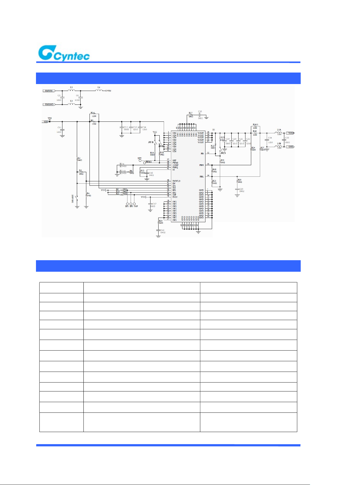
BOM LIST:
Table 10: The BOM without EMI solution
COUNT REF DES DESCRIPTION
1 U1 VPN12AD02-FUV
2 C12, C14, MLCC, 10uF, 50V, X7R, 1210
2 C20, C22 MLCC, 22uF, 25V, X7R, 1206
1 C11 E-cap, 82uF, 50V
1 C24 E-cap, 270uF, 16V
1 C17 MLCC, 10uF, 10V, X7R, 0805
1 C10 MLCC, 2.2nF, 25V, X7R, 0402
1 C25 MLCC, 4.7nF, 16V, X7R, 0402
1 C15 MLCC, 22nF, 16V, X7R, 0402
1 R28 RES, 5.6Kohm, 0402 1%
2 R2, R16, R18 RES, 10Kohm, 0402 1%
2 R9, R10 RES, 100Kohm, 0402 1%
1 R8 RES, 1Kohm, 0402 1%
1 R22 RES, 14Kohm, 0402 1%
2 R23 RES, 1.5Kohm, 0402 1%
1 R1, R12 RES, 30Kohm, 0402 1%
1 R4, R24 RES, 0ohm, 0402
1 R20 RES, 150ohm, 0402 1%
1 R21 RES, 12.4Kohm, 0402 1%
6 R5, R5-1, R26,
R26-1, JR16, JR18
Short
16
L2, L6, C3, C9,
C13, C16, C18,
C19, C21, C23,
R11, R17, R19,
R25, R27, JR25
NC