Daewoo DV-F24S User manual

DAEWOO ELECTRONICS CO., LTD.
Service Manual
MODEL: DV-F24S/F44S
DV-F26S/F46S
DV-F28S/F48S
PAL/MESECAM/SECAM
MARCHE EJECT
ENR./IMM.
CAN/ALIGN
R.R. AV.R.
LECTURE
STOP
•
MARCHE
EJECT ENR./IMM. R.R. AV.R.
LECTURE
STOP
CAN/ALIGN
•
+ CHAINE – ENR.
R.R. AV.R.
STOP LECTUREEJECTMARCHE
✔
Caution
: In this Manual, some parts can be changed for improving, their
performance without notice in the parts list. So, if you need the
latest parts information,please refer to PPL(Parts Price List) in
Service Information Center (http://svc.dwe.co.kr).

SPECIFICATIONS
GENERAL
Power requirement : AC 230V, 50Hz
Power consumption : Typical 18W (in REC mode)
Temperature : 5°C~35°C (Operating)
–20°C~60°C
(Storage temperature)
Operating position : Horizontal only
Dimensions (WxHxD) : 360X90X332 (mm)
Weight : Approx. 5.0Kg
Format : VHS standard
Tape width : 12.65mm
Tape speed : (SP): 23.39 mm/sec
(LP): 11.70 mm/sec (4HEAD)
Maximum recording time
with full-size cassette : (SP): 240 min. with E-240
video cassette
(LP): 480 min. with E-240
video cassette (4HEAD)
Maximum recording time
with full-size cassette : (SP): 45 min. with EC-45
cassette
(LP): 90 min. with EC-45
cassette (4HEAD)
VIDEO
Signal system : PAL/SECAM colour and CCIR
monochrome signals,
625 lines/50 fields
Recording system : Rotary two-head helical scan
with a slant double-azimuth
combination video head
(4HEAD)
Input : 1.0 Vp-p, 75 ohms, unbalanced
Output : 1.0 Vp-p, 75 ohms, unbalanced
Signal-to noise ratio : 45 dB (Rohde & Schwarz noise
meter) with NETTETE IMAGE
control at center position
Horizontal resolution : 240 lines with NETTETE IMAGE
control at center position
AUDIO
Recording system : Longitudinal track
Input : –8 dBs, (CENELEC standard),
more than 47 k-ohms,
unbalanced
Output : –6 dBs, (CENELEC standard),
less than 1 k-ohm, unbalanced
(100 k-ohms, load)
Frequency range : 100 Hz to 8,000 Hz
Signal to noise ratio : 40 dB (More than)
TUNER
Tuning system : Voltage synthesized tuner
Programmable V/S 59 CH
(99 CH option) (Hyper band)
RF Output : UHF channel 36
(Adjustable 30~39)
TIMER
Memory programmable
59 CH (99 CH option)
Back up time : More than 30 minutes
Clock exactness : In accordance with the exactness
of power supply frequency (50Hz)
ACCESSORIES
Provided Accessories : Remote control unit
RF Cable, Batteries
* Design and specifications can be subjected to change
without notice.

1
• Safety Check after Servicing
Examine the area surrounding the repaired location for damage or deterioration. Observe that screws, parts and wires
have been returned to original positions. Afterwards, perform the following tests and confirm the specified values in order
to verify compliance with safety standards.
1. Insulation resistance test
Confirm the specified insulation resistance between power cord plug prongs and externally exposed parts of the set
(RF terminals, antenna terminals, video and audio input and output terminals, microphone jacks, earphone jacks, etc.) is
greater than values given in table 1 below.
2. Dielectric strength test
Confirm specified dielectric strength between power cord plug prongs and exposed accessible parts of the set (RF
terminals, antenna terminals, video and audio input and output terminals, microphone jacks, earphone jacks, etc.) is
greater than values given in table 1 below.
3. Clearance distance
When replacing primary circuit components, confirm
specified clearance distance (d), (d') between soldered
terminals, and between terminals and surrounding
metalic parts. See table below.
Table 1: Rating for selected areas
* Class II model only.
Note: This table is unofficial and for reference only. Be sure to confirm the precise values for your particular country and
locality.
4. Leakage current test
Confirm specified or lower leakage current between B (earth ground, power cord plug prongs) and externally exposed
accessible parts (RF terminals, antenna terminals, video and audio input and output terminals, microphone jacks,
earphone jacks, etc.)
Measuring Method: (Power ON)
Insert load Z between B (earth ground, power cord plug
prongs) and exposed accesible parts. Use and AC
voltmeter to measure across both terminals of load Z.
See figure 2 and the following table.
Table 2: Leakage current ratings for selected areas
Note: This table is unofficial and for reference only. Be sure to confirm the precise values for your particular country and
locality.
Fig. 2
AC Line Voltage Region Insulation Dielectric Clearance
Resistance Strength Distance (d), (d')
100V Japan ≥1 MΩ/500 V DC 1kV AC 1 minute ≥3 mm
110 to 130V USA & – – – 900V AC 1 minute ≥3.2mm
Canada
* 110 to 130 V Europe ≥4 MΩ/500 V DC 3 kV AC 1 minute ≥3 mm (d)
200 to 240 V Australia ≥6 mm (d')
(a: Power cord)
AC Line Voltage Region Earth Ground
Load Z Leakage Current ( i)(B) to:
100V Japan i≤1 m A rms Exposed accessible
parts
110 to 130 V USA & i≤0.5 m A rms Exposed accessible
Canada parts
i≤0.7 m A peak Antenna earth
110 to 130 V Europe i≤2 m A dc terminals
200 to 240 V Australia i≤0.7 m A peak Other terminals
i≤2 m A dc
Fig. 1
1k
1.5k
1.5kµF
2k
50k
d
Primary circuit termimals
Chassis
d'
a
Z
Exposed
accessible
part AC Voltmeter
(high impedance)
Earth Ground
power cord plug prongsB

TABLE OF CONTENTS
SECTION 1. CONTROLS AND FUNCTIONS...........................................................................................................3
SECTION 2. ELECTRICAL ADJUSTMENTS
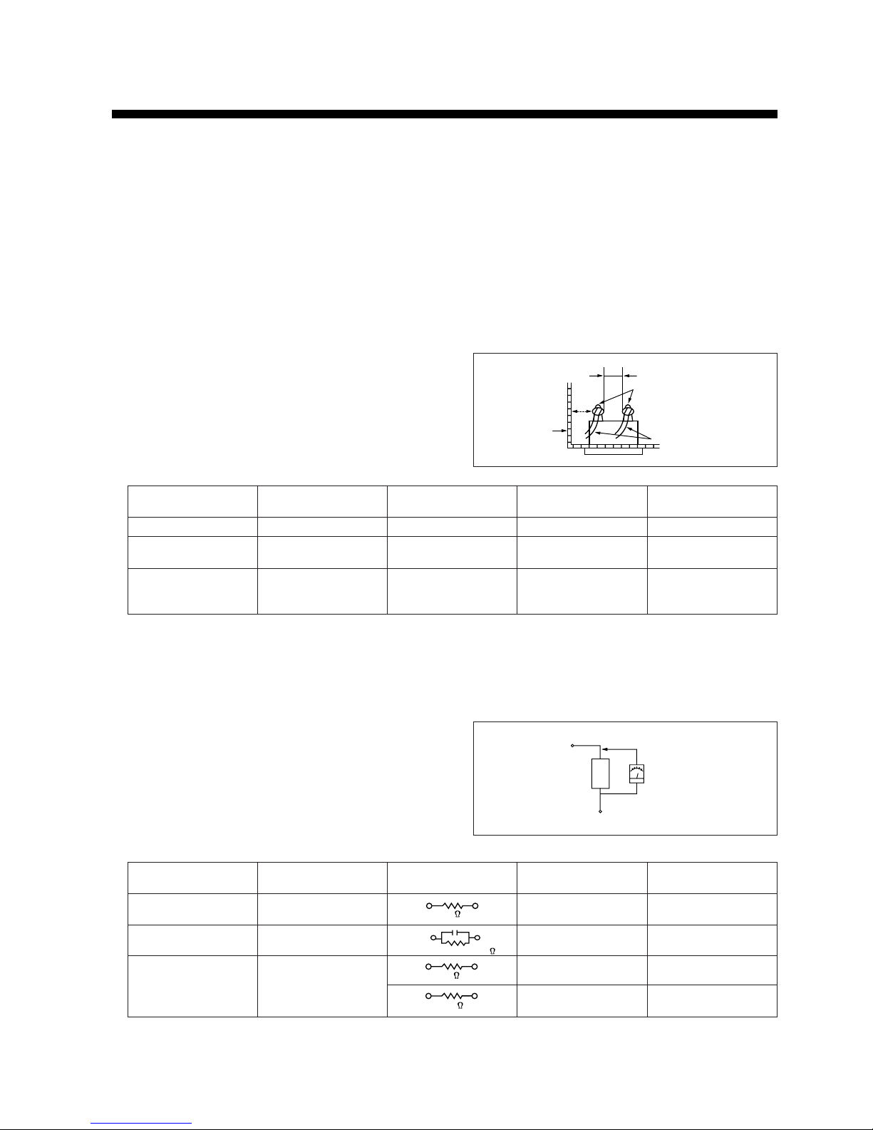
2-1. VIDEO CIRCUIT ADJUSTMENT METHODS.....................................................................................................................5
2-2. AUDIO CIRCUIT ADJUSTMENT METHOD.......................................................................................................................7
2-3. IF MODULE CIRCUIT ADJUSTMENT METHODS............................................................................................................8
SECTION 3. CIRCUIT OPERATION PRINCIPLES
3-1. POWER CIRCUIT..............................................................................................................................................................12
3-2. VIDEO CIRCUIT................................................................................................................................................................14
3-3. IF CIRCUIT OPERATION..................................................................................................................................................19
SECTION 4. TROUBLE SHOOTING FLOW CHART
4-1. POWER CIRCUIT..............................................................................................................................................................21
4-2. PIF CIRCUIT TROUBLE SHOOTING...............................................................................................................................23
4-3. LOGIC CIRCUIT................................................................................................................................................................24
4-4. SERVO-SYSCON CIRCUIT..............................................................................................................................................26
4-5. AUDIO CIRCUIT................................................................................................................................................................34
4-6. VIDEO CIRCUIT................................................................................................................................................................36
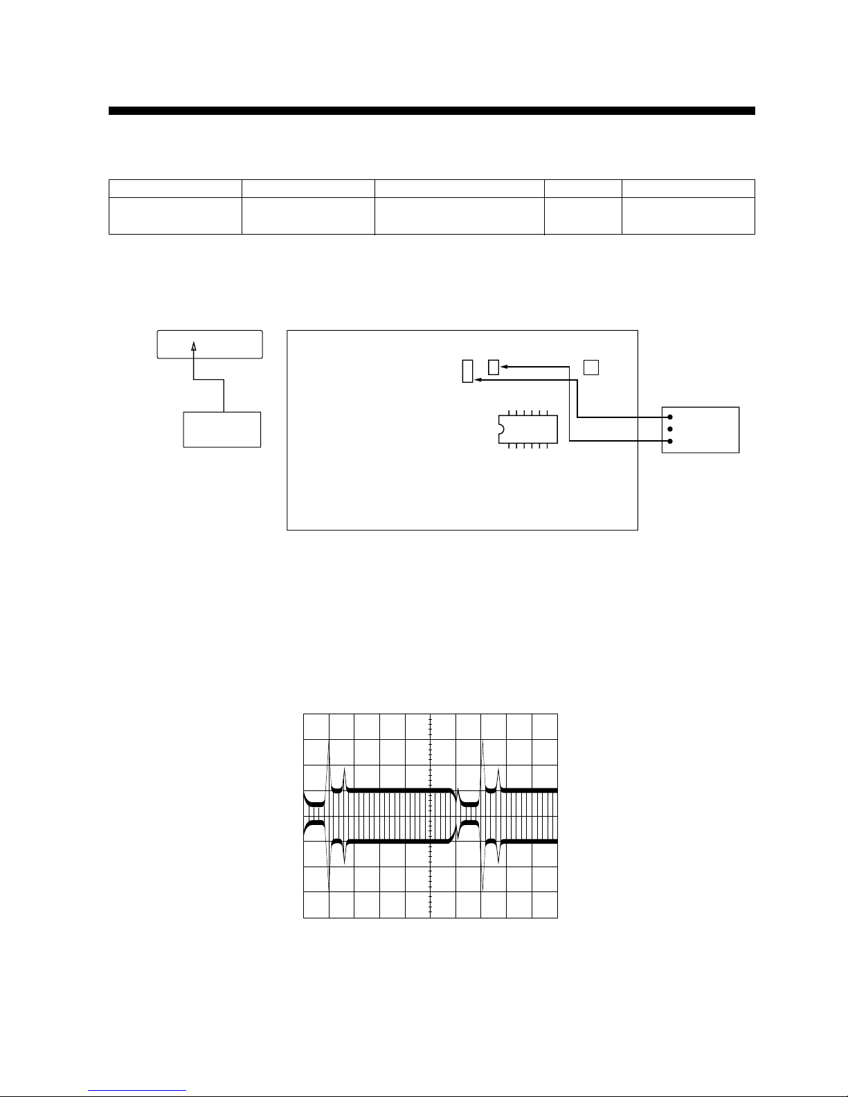
SECTION 5. WAVEFORMS OF THE VIDEO CIRCUIT......................................................................................47
SECTION 6. µ-COM PORT DESCRIPTION............................................................................................................51
SECTION 7. CIRCUIT DIAGRAM
7-1. CONNECTION DIAGRAM................................................................................................................................................57
7-2. POWER CIRCUIT..............................................................................................................................................................58
7-3. MAIN CIRCUIT..................................................................................................................................................................59
7-4. LOGIC CIRCUIT................................................................................................................................................................60
7-5. VIDEO CIRCUIT................................................................................................................................................................61
7-6. 2 HEAD PRE AMP CIRCUIT.............................................................................................................................................62
7-7. 4 HEAD PRE AMP CIRCUIT.............................................................................................................................................63
7-8. SECAM COLOUR CIRCUIT.............................................................................................................................................64
7-9. AUDIO CIRCUIT................................................................................................................................................................65
7-10. IF MODULE CIRCUIT.....................................................................................................................................................66
7-11. PIF CIRCUIT....................................................................................................................................................................67
7-12. SW & SCART CIRCUIT...................................................................................................................................................68
7-13. OSD CIRCUIT.................................................................................................................................................................69
7-14. REMOTE CONTROL CIRCUIT (VR-F2B).......................................................................................................................70
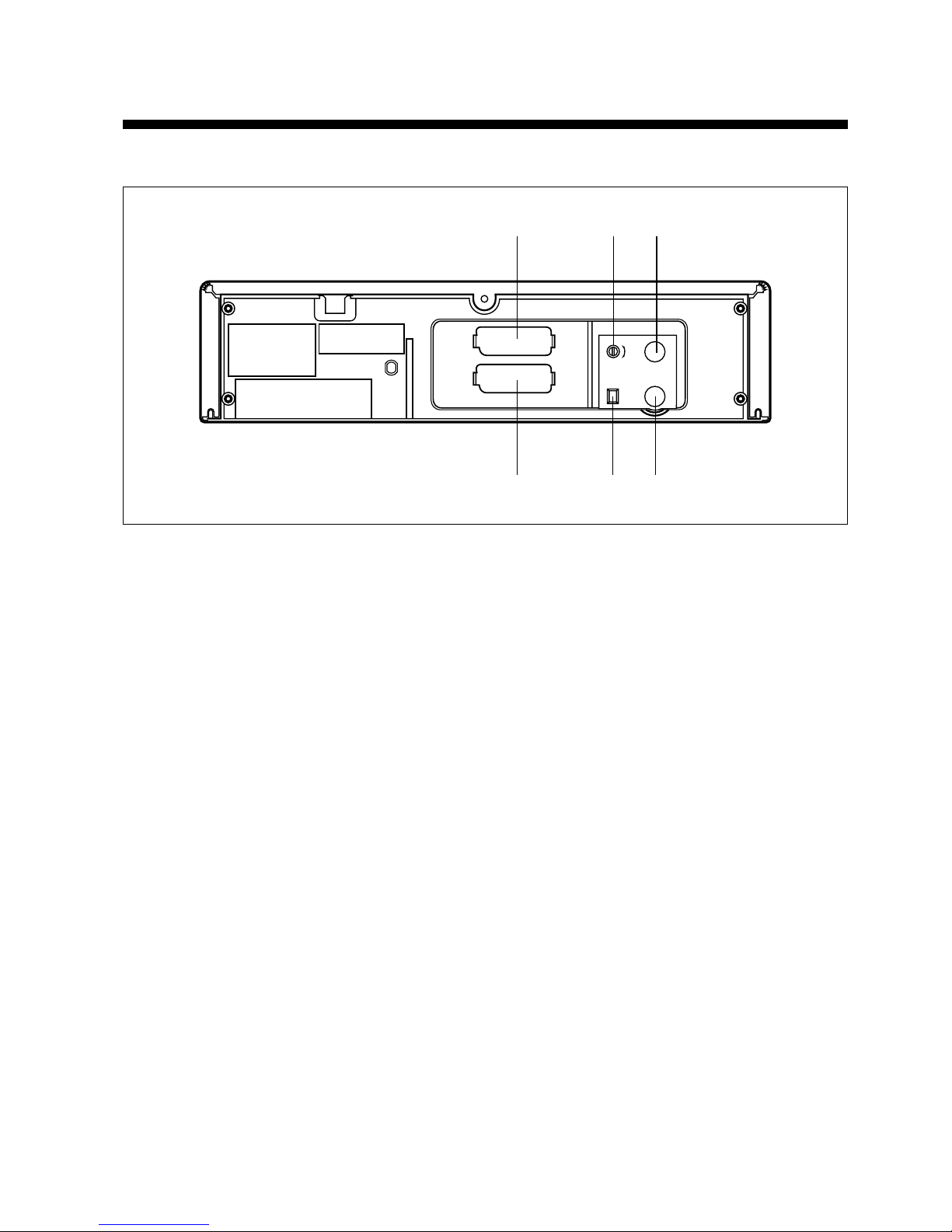
SECTION 8. COMPONENTS LOCATION GUIDE ON PCB (BOTTOM VIEW)
8-1. PCB MAIN.........................................................................................................................................................................71
8-2. PCB POWER.....................................................................................................................................................................72
8-3. PCB PRE AMP (4HEAD)...................................................................................................................................................72
8-4. PCB PRE AMP (2HEAD)...................................................................................................................................................72
8-5. PCB VIDEO.......................................................................................................................................................................73
8-6. PCB IF MODULE..............................................................................................................................................................73
8-7. PCB AV & SCART.............................................................................................................................................................73
8-8. PCB LOGIC.......................................................................................................................................................................74
SECTION 9. DISASSEMBLY
9-1. PACKING ASS'Y...............................................................................................................................................................76
9-2. FRONT PANEL ASSEMBLY.............................................................................................................................................77
9-3. SET TOTAL ASSEMBLY ..................................................................................................................................................80
9-4. INSTRUMENT DISASSEMBLY........................................................................................................................................81
9-5. JIG PCB CONNECTION DIAGRAM.................................................................................................................................89
SECTION 10. ELECTRICAL PART LIST...................................................................................................................90
2

3
SECTION 1. CONTROLS AND FUNCTIONS
MARCHE EJECT
ENR./IMM.
CAN/ALIGN
R.R. AV.R.
LECTURE
STOP
•
!@ #$% &
*^(
FRONT
1. F24S/F44S SERIES
MARCHE
EJECT ENR./IMM. R.R. AV.R.
LECTURE
STOP
CAN/ALIGN
•
!@ #$%*(
&^
2. F26S/F46S SERIES
+ CHAINE – ENR.
R.R. AV.R.
STOP LECTUREEJECTMARCHE
!@ &^
(*%#$
3. F28S/F48S SERIES

4
AUX/POU
R
TV
DECODEU
R
CH.H
CH.L
TEST
ON
OFF
SORTIE
ANTENNE
ENTREE
ANTENNE
)
1 3
2
4
5
REAR
!POWER ON/OFF
@EJECT
#CHANNEL SELECTION ¡
$CHANNEL SELECTION ¡
%RECORD AND OTR
(ONE TOUCH TIMER RECORDING)
^PLAY
&STOP
*REWIND/REVIEW
(FAST FORWARD/CUE
)AUX/POUR TV JACK
1DECODER JACK
2RF OUTPUT CHANNEL ADJUSTMENT SCREW
3TEST SIGNAL ON/OFF SWITCH
4ANTENNA INPUT TERMINAL
5ANTENNA OUTPUT TERMINAL

5
SECTION 2. ELECTRICAL ADJUSTMENTS
2-1. VIDEO CIRCUIT ADJUSTMENTS METHODS
1. REC EQ ADJUSTMENT
• Connection Method
• Adjustment Procedure
1) Set the INPUT mode to LINE mode.
2) Supply the SECAM MAGENTA signal to the VIDEO IN TERMINAL.
3) Set the VCR to the STOP mode.
4) Connect the oscilloscope to TJ401 and trigger the scope with the composite sync at TJ313
5) Adjust RL491 in order to correspond with MAGENTA EDGE section
Adj. Location Checking Point Measuring Equipment Mode INPUT SIGNAL
RL491 TJ401 Signal Gen, Oscilloscope STOP SECAM MAGENTA
signal
TJ401 TJ313 RL491
ICL01
VIDEO PCB
VIDEO SET
SECAM MAGENTA
Signal
TOP VIEW
CH-1
OSCILLOSCOPE
CH-2
SIGNAL
GENERATOR
Horizontal: 10µs/div
vertical : 500mv/div

6
2. PB EQ ADJUSTMENT
• Connection Method
• Adjustment Procedure
1) Set the INPUT mode to LINE mode.
2) Playback the SECAM test tape (DS-1).
3) Set the VCR to PLAY mode.
4) Connect the Oscilloscope to TJ402 and trigger the scope with the composite sync at TJ313.
5) Adjust RL492 in order to correspond with MAGENTA EDGE section.
TJ402 TJ313 RL492
ICL01
CH-1
OSCILLOSCOPE
CH-2
TOP VIEW
VIDEO PCB
Adj. Location Checking Point Measuring Equipment Mode Test Tape
R492 TJ402 Signal Gen, Oscilloscope PLAY DS-1
Horizontal: 10µs/div
vertical : 100mv/div

7
2-2. AUDIO CIRCUIT ADJUSTMENT METHOD
1. AUDIO RECORD BIAS
• Connection Method
• Adjustment Procedure
1) Set the INPUT mode to LINE mode.
2) Disconnect any input
3) Connect the Audio level meter to both TP1 and TP2
4) After inserting a blank tape, record in SP mode.
5) Adjust R292 to obtain 3.0 mVrms.
TOP VIEW
R292
3.0mVrms
+
–
A/C HEAD
TP2
(–)
TP1
(+)
Audio LEVEL METER
MAIN PCB
Adjustment Parts Checking Point Measuring Equipment MODE INPUT SIGNAL
R292 A/C Head PCB Audio level meter REC No signal
TP1(+), TP2(-)

2-3. IF MODULE CIRCUIT ADJUSTMENT METHODS
1. PAL/SECAM-L HIGH BAND AFT
• PAL/SECAM HIGH BAND AFT
IF MODULE PCB (TOP VIEW)
• Adjustment Procedure
1) Connect the attached circuit to PIN !of P102.
2) Supply +12V to PIN$, +5V to PIN%and GND to PIN@ of P101.
3) Supply +5V to PIN# of P101and +5V to PIN%of P102. (SECAM-L MODE)
4) Connect the signal generator output to PIN!, and GND to PIN@ of P101.
5) Connect the oscilloscope probe to check point.
6) Adjust L102 to obtain 2.5V ±0.15V DC Voltage at check point.
ADJUSTMENT PARTS
CHECK POINT TEST EQUIPMENT INPUT SIGNAL
P102 Signal Gen. Refer to
L102 PIN!Oscilloscope the
Power Supply following.
2.5V ± 0.15V DC
Q110 Q106
Z104
R192
R191 Z101
IC102
Q101
Q102
R193
L102
P102
#5 #2 #1
Z102
P101
#5 #4 #3 #2
#1
#2
#4
2.2µ/50V 56K 2.2µ/50V
27K
15K
+12V
0.47µ/50
10K
+5V TEST CIRCUIT
for AFT and RF AGC
adjustment.
CH1
OSCILLOSCOPE
#1
0.5 mS/DV
50 mV/DIV (10:1)
10K
Modulation method: 30% AM
Af: 400 Hz
fc: 38.9 MHz
Signal Level: 80 dBuV
SIGNAL GEN.
GND
OUTPUT
8

9
2. PHASE
• PHASE
IF MODULE PCB (TOP VIEW)
• Adjustment Procedure
1) Connect the attached circuit to PIN !of P102.
2) Supply +12 to PIN$, +5 to PIN%and GND to PIN@ of P101.
3) Supply +5 to PIN# of P101 and to PIN%of P102. (SECAM-L MODE)
4) Connect the signal generator output to PIN!, and GND to PIN@ of P101.
5) Connect the oscilloscope probe to check point.
6) Adjust R192 to obtain minimum RIPPLE at check point.
Q110 Q106
R192
R191 Z101
IC102
Q101
Q102
R193
L102
P102
#5 #2 #1
Z102
P101
#5 #4 #3 #2
#1
#2
#4
2.2µ/50V 56K 2.2µ/50V
27K
15K
+12V
0.47µ/50
10K
+5V TEST CIRCUIT
for AFT and RF AGC
adjustment.
CH1
OSCILLOSCOPE
#4
0.5 mS/DV
50 mV/DIV (10:1)
10K
Modulation method: 100% AM
Af: 400 Hz
fc: 38.9 MHz
Signal Level: 80 dBuV
SIGNAL GEN.
GND
OUTPUT
MINIMUM RIPPLE
IC101
#4
ADJUSTMENT PARTS
CHECK POINT TEST EQUIPMENT INPUT SIGNAL
P102 Signal Gen. Refer to
R192 PIN$Oscilloscope the
Power Supply following.

10
3. SECAM-L ACCENT AFT
• SECAM-L ACCENT AFT
IF MODULE PCB (TOP VIEW)
• Adjustment Procedure
1) Connect the attached circuit to PIN !of P102.
2) Supply +12V to PIN$, +5V to PIN%and GND to PIN@ of P101.
3) Supply GND to PIN#of P101 and +5V to PIN%of P102 (SECAM-L ACCENT MODE)
4) Connect the signal generator output to PIN!, and GND to PIN@ of P101.
5) Connect the oscilloscope probe to check point.
6) Adjust R193 to obtain 2.5V ± 0.15V DC voltage at the check point.
2.5V ± 0.15V DC
Q110 Q106
R192
R191 Z101
IC102
Q101
Q102
R193
L102
P102
#5 #2 #1
Z102
P101
#5 #4 #3 #2
#1
#2
#4
2.2µ/50V 56K 2.2µ/50V
27K
15K
+12V
0.47µ/50
10K
+5V TEST CIRCUIT
for AFT and RF AGC
adjustment.
CH1
OSCILLOSCOPE
#1
0.5 mS/DV
50 mV/DIV (10:1)
10K
Modulation method: 30% AM
Af : 400 Hz
fc: 34.3 MHz
Signal Level: 80 dBuV
SIGNAL GEN.
GND
OUTPUT
IC1O1
ADJUSTMENT PARTS
CHECK POINT TEST EQUIPMENT INPUT SIGNAL
P102 Signal Gen. Refer to
R193 PIN!Oscilloscope the
Power Supply following.

11
4. RF AGC
• RF AGC
IF MODULE PCB (TOP VIEW)
• Adjustment Procedure
1) Connect the attached circuit to PIN @of P102.
2) Supply +12V to PIN$, +5V to PIN%and GND to PIN@ of P101.
3) Supply +5V to PIN# of P101and to PIN%of P102. (SECAM-L MODE)
4) Connect the signal generator output to PIN!, and GND to PIN@ of P101.
5) Connect the oscilloscope probe to check point("A" POINT).
6) Adjust R191 to obtain 6.0V ± 0.2V DC at the check point ("A" POINT).
6.0V ± 0.2V DV
Q110 Q106
R192
R191 Z101
IC102
Q101
Q102
R193
L102
P102
#5 #2 #1
Z102
P101
#5 #4 #3 #2
#1
#2
#4
2.2µ/50V 56K
27K
15K
+12V
0.47µ/50
10K
+5V TEST CIRCUIT
for AFT and RF AGC
adjustment.
10K
Modulation method: 30% AM
Af: 400 Hz
fc: 38.9 MHz
Signal Level: 92 dBuV
SIGNAL GEN.
GND
OUTPUT
CH1
OSCILLOSCOPE
0.5 mS/DIV
100 mV/DIV (10:1)
A
2.2µ/50V
ADJUSTMENT PARTS
CHECK POINT TEST EQUIPMENT INPUT SIGNAL
"A" POINT Signal Gen. Refer to
R191 Oscilloscope the
Power Supply following.

12
SECTION 3. CIRCUIT OPERATION PRINCIPLES
3-1. POWER CIRCUIT
1. Basic Operation
The input voltage is rectified by the bridge diode (D801) and the capacitor (C807), ie, it is converted from AC to DC.
This voltage drives the gate of the FET (Q801) via the 'motive stage' (gate drive circuit) when the gate drive voltage exceeds
Vgs(th), it makes the FET turn on. However the mains input voltage can range from 110-220V ac, depending on country.
Therefore the voltage driving the FET'S gate can range correspondingly.
The circuit is designed to work for all input/output voltages, ie, Vgs>Vgs(th) for minimum input voltage.
When the FET is first turned on by the driver stage, the voltage in coil B is Vi(dc)*Nb/Np. This increases Vgs via C811,
increasing FET current and so increasing the energy stored in coil B. During a switching cycle, the FET is switched off by the
actions of voltage drop of components D803 and R806 combined with the switching control circuit.
When Q801 is switched off, the energy stored in the primary side is transmitted to the secondary side and so the output
voltage is generated. Once the power in the secondary (output) side starts dropping, this triggers the drive stage via the
back emf in the transformer and so the FET is switched on. At this time the negative voltage at C811 from the B coil is
rectified by D804 and the power is dissipated by R812. The transistor of opto-isolator IC801 is switched on drawing current
Ic away from the gate of FET Q801 and so switching the FET off.
Since the power transmitted to the secondary side is of high frequency, a fast recovery diode or Schottky barrier diode is
used for rectification. The voltage is smoothed using electrolytic capacitors which have a low impedence at the switching
frequency.
2. Snubber Circuit
The snubber circuit suppresses any sudden voltage rise when the FET turns on and keeps Vds (drain-source voltage of
FET) at a safe level. It also reduces noise in the FET.
In this snubber circuit (ie C808, D802, R807, C809, L804), once the FET is switched off, the energy of that part of the
transformer is transferred to C808 and R807. Because of factors such as lead inductance of each element, resistance of the
capacitor circuit, frequency characteristics of the parasitics, we can only do an approximate analysis. As the diode D802
has a short recovery time, the reverse current can be disregarded.
R803
VIN VG
R804
R806
R824
C824 R808 R809
Vgs = Gate–Source voltage
Vgs(th) = Gate–Soure threshold voltage
< Drawing 1: motive/driving stage of circuit >
R811
C808
D802
R807
C809
L804
< Drawing 2: snubber circuit >

13
(i) Evaluation of resistance
I2 *R = 0.5 * Li *(Idp)2*F=Vc2/R
R=2Vc 2/(0.025Lp *(Idp)2*F)
(on average, the experimental value of Li=0.025 Lp is found)
(ii) Evaluation of capacitance
Li *(Idp)2/2=C *(1.2Vdc-Vdc)2
C=25Lp *(Idp)2/40 *(Vdc)2
(iii) Power consumption in resistance
Pr=Li *(Idp)2*F/2
Idp=peak value of drain current
1.2 Vdc=voltage of surge absorption capacitor
Vdc=voltage input to snubber
F=minimum oscillation frequency
Li=leakage inductance (<Lp=primary inductance)
* In a normal snubber circuit, the time constant is chosen to be 20 times greater than the switching period.
3. Voltage control/regulation
The circuit in drawing 3 to that in drawing 4, it can be seen that
Vr=R822 *Vo/(R819+R822)
The voltage Vr changes in proportion to the change in output voltage (ie, Ever 6V). These changes are fed back to the
primary side via the opto-isolator to the switching control circuit which controls how long the FET is switched on (and the
duty cycle of the FET). Thus we have voltage regulation.
If Vr exceeds 2.5V because Vo increases, the internal transistor of the shunt regulator will be switched on and the shunt
regulator will hold the voltage at Vk. In addition, the increase in the diode current of the opto-isolator will raise the collector
Ic of the opto-isolator primary side. This current makes the base current, Ib, of Q802 and Q803 increase, making the gate
voltage of the FET drop. This causes the on-time of the FET to decrease and so makes the output voltage Vo decrease.
If Vr is below 2.5V, the opposite will happen.
!
@
R817
100 R818
220
R821
1K C821
0.47µ/50V
IC802
KIA431
R822
3.3K(F)
R819
4.7K(F)
Reference
(R)
2.5Vref
+
–
Anode(A)
Cathode
(K)
Reference
(R)
Cathode
(K)
Anode
(A)
< Drawing 3: voltage control circuit >
< Drawing 4: block diagram of shunt regulator >
+

14
3-2. Video Circuit (The operating principles of the video circuit)
1. The signal flow
A. Signal flow of the luminance system in the REC mode.
The recording Video Signal (composite video signal) is input to the AGC amplifier through Pin 12 of IC301, and the sync
signal level is kept constant.
The video AGC circuit is used to keep the amplitude of video signal constant, and two types of AGCs, "SYNC AGC+PEAK
AGC" are incorporated. The switching point for changing from SYNC. AGC to PEAK AGC is set at 110% white level of the
input video signal. The video level at Pin 4 of IC301 becomes 0.5Vp-p when a standard video signal (1Vp-p) is applied to Pin
12 of IC301.
The signal from the AGC circuit is input to the Video AMP circuit through the QV/QH circuit. This Video AMP circuit amplifies
input video signal by about 6dB, and then is input to the buffer (composed of Q309 and R323) through Pin 16 of IC301.
The other signal is as follows:
The chrominance component in the AGC circuit is filtered by a LPF (Low Pass Filter) and the luminance signal (eliminated
chrominance) is fed to the YNR circuit.
In the circuit, vertical enhancing is used for the luminance signal, using an external 1H Delayline (CCD IC: LC89970), and its
output is fed to Pin 4 of IC301. The output signal from Pin 4 of IC301 is input to Pin 5 through the subemphasis circuit. This
signal is then fed to emphasis circuit (consists of Detail Enhancer, Non-linear Emphasis and MAIN Emphasis). then the high
frequencies of the output signal are enhanced by this Emphasis circuit.
This signal is fed to the FM Modulator, and the recording Y-FM signal is obtained from Pin 2 of IC301.
This signal is input to the PREAMP IC (Pin 8 of LA7411: 2 Head, Pin 11 of LA7416: 4 Head).
Video
AGC QV/QH Video
AMP
LPF YNR Sub-
emphasis
buffer
CLAMP
IH DELAY CCD
IC302
REC
EQ FM
MOD MAIN
EMPHA NL
EMPHA
CARRIER
SHIFT
To. PREAMP CIRCUIT
LA7411 *PIN INPUT
LA7416 1PIN INPUT
Video input
2 6
buffer
To OSD
$ %
*^
80
@
*&^
BLOCK1. Luminance signal flow in the record mode.
fsc : 4.433619MHz

15
B. Signal flow of the PAL colour in the record mode
A recording composite video signal is fed to the AGC circuit from Pin 12 of IC301, and its output signal is passed through a
BPF (Band Pass Filter) to eliminate the luminance components, and then only the colour signal is fed to the ACC (Auto
Colour Controller) amplifier. The gain of the ACC amplifier is controlled by the DC voltage at Pin 41 of IC301.
The signal from ACC AMP is fed to the Main Converter to transfer 4.43MHz to 627KHz. That is, the summation and
substraction of the two input signal frequencies are obtained from this Main Converter. Here, the two input signal
frequencies are 4.43MHz and 5.06MHz. The output frequencies from the Main Converter are approximately 627KHz and
9.49MHz. The output from the Main Converter is fed to the killer circuit through the LPF. The LPF is used to eliminate
unwanted frequencies (ie: 9.49MHz).
The Killer detector gives a reliable operation thanks to the application of both systems i.e. synchronized detection (APC
Killer) and the Peak detection (ACC Killer) in the record mode. The signal is obtained from Pin 38 of IC301 as the recording
colour signal. The output signal from Pin 38 of IC301 is fed to the PREAMP IC (2 Head: Pin 7 of LA7411, 4 Head: Pin 10 of
LA7416).
C. Signal flow of the luminance in the playback mode
The playback Y-FM from the PREAMP (approximately 60dB amplification) is fed to the PB EQ circuit to perform frequency-
limiting and phase compensation. The output signal from the PB EQ circuit is input to Pin 1 of IC301 and then this signal is
passed through the FM-AGC so that the signal level is kept constant. The output signal is fed to a Double Limiter. The
Double Limiter's function is as follows:
As the high frequency components of the playback Y-FM signal are deteriorated due to the characteristics of the Tape-
Head system, Y-FM signal (black spike) effect may be seen in the playback picture, and the Double Limiter is used to
compensate for this.
The signal from the Double Limiter is fed to an FM Demodulator. This demodulated video signal is passed through the LPF
and the emphasized high frequency component from the Main Emphasis is de-emphasized. The signal from the Main DE-
emphasis is fed to pin 4 of IC301.
Video input
2
Video
AGC BPF ACC
AMP MAIN
CONV IMHz
LPF
Killer
4.43MHz 4.43MHz
(5.06±4.43)
MHz
5.06MHz
O
u
I
To. PREAMP
2Head: Pin
&
of LA7411
4Head: Pin
)
of LA7416
BLOCK 2. PAL COLOUR SIGNAL FLOW
627KHz

16
This signal from Pin 4 of IC301 is then passed through a sub-deemphasis and Buffer and fed to Pin 5 of IC301.
The signal input to Pin 5 of IC301 is fed to the YNR through a LPF. The YNR circuit gives considerable noise reduction
effects. The signal from the YNR circuit is fed to the Y/C Mixer circuit through the Non-linear Deemphasis, the Double High
Pass Noise Canceller (DHPC), and the Picture Controller circuit. The signal is then mixed with the playback colour signal
and the PB Video Signal is obtained from Pin 16 of IC301 through Quasi-Vertical/Quasi-Horizontal (QV/QH) Insertion circuit
and the Video Output Amplifier (about 6dB amplification). The output of Pin 16 (approximately 2Vp-p) is input to the Buffer
circuit (consists of Q309 and R323).
D. Signal flow of the PAL colour in the playback mode
FM
AGC Double
Limiter FM
Demod L P F Main
De-empha
L P F Sub-deempha
& buffer
Y N R N L
De-empha Double HP
Noise Can Picture
Controller
IH Delay
CCD
IC302
Video
AMP QV/QH Y/C
MIX
R322
R323
Q309 TO OSD CIRCUIT
6
$
%
%
0
*
8
!
Y-FM input
BLOCK 3. PLAYBACK LUMINANCE SIGNAL FLOW
Buffer
1.3MHz
LPF
PB colour input
uACC
AMP Main
Conv 4.43MHz
BPF
627KHz 627KHz
5.06MHz
± 627KHz
NAP PB AMP
/Killer 2H Delay
IC302
Y/C
Mixer
+=
$
@
“
q
E
wFrom. PB luminance
signal
5.06MHz
fsc (4.433619MHz)
PB SECAM
Colour input
BLOCK 4. PB PAL COLOUR SIGNAL FLOW
4.43MHz
4.43MHz
IC303
!
)
PAL : LOW
MESECAM : HIGH

17
The signal from the PREAMP circuit is fed to Pin 38 of IC301 and then this signal is amplified by 60dB (almost 1000 times).
The signal from Pin 38 of IC301 is filtered by the LPF. That is, the LPF is used to eliminate the luminance signal. The down-
converted colour signal (627KHz) from the LPF is fed to the Main Converter through the ACC amplifier circuit. The output
from the Main Converter is fed to Pin 23 and 24 of IC301 through a BPF (4.43MHz). The colour signal frequency of Pin 24 of
IC301 is 4.433619MHz. The output signal at Pin 24 of IC301 (LA7437) is input to Pin 1 of IC303 (LA7356: SECAM
DETECTOR) in order to detect whether the colour signal is PAL or MESECAM. After filtering out the crosstalk components
by an external CCD IC (LC89970), this signal is input to Pin 26 of IC301. The output of Pin 26 is fed to Pin 29 of IC301
through a PB AMP/Killer and NAP circuit. The colour signal from Pin 29 is fed to the Y/C Mixer through Pin 28.
E. Signal flow of the SECAM colour in the record mode
The video signal is input to a 4.3MHz BPF through Pin 1 of ICL01 (BA7207S: SECAM colour). The signal at Pin 1 is fed to
the REC BELL circuit to be de-emphasized.
The REC BELL output is then fed to Pin 26 of ICL01.
This signal is input to Pin 1 of ICL02 (LA7356: SECAM DETECTOR) and Pin 24 of ICL01 (BA7207S)
The signal input to Pin 1 of ICL02 is used to detect whether the signal is SECAM or non-SECAM. If this signal is the SECAM
colour, the voltage at Pin 10 of ICL02 is high (almost 4.0 volts). If not, the voltage at Pin 10 of ICL02 is low.
The other signal from Pin 26 of ICL01 is fed to Pin 24 of ICL01 through the 12dB AMP circuit (consists of RL425, RL426,
RL427, RL428, RL429, CL429 and QL413). The signal from Pin 24 is fed to the Limiter. In this Limiter circuit, the output
amplitude is limited. The Limiter output is fed to a 1/4 divider circuit in order for the colour signal to be divided by 4. This
signal is then fed to the REC SYNC GATE circuit. The noise of the SYNC part is removed by the REC SYNC GATE. The
REC SYNC GATE output is fed to the 1.1MHz BPF so that the unwanted signal can be eliminated. The 1.1MHz BPF output
is fed to Pin 28 of ICL01 through the REC EQ circuit.
4.3 MHz
BPF REC
BELL Main
De-empha
1/4 Divider Limiter 12dB
AMP
q!
PB colour input
=
REC
SYNC GATE
1.1 MHz
BPF REC
EQ =REC SECAM
BLOCK 5. RECORD SECAM COLOUR SIGNAL FLOW

18
F. Signal flow of the SECAM colour in the playback mode
The output signal (mixed luminance and colour) from the head is input to the PREAMP IC. This signal is amplified by about
60dB (approximately 1000 times) by the preamp IC. The signal from the PREAMP IC is fed to 1.1MHz BPF circuit (consists
of CL421, RL410, LL408, CL408 and RL411). The luminance signal is eliminated by the 1.1MHz BPF circuit. This output
signal is fed to Pin 18 of ICL01. The output at Pin 18 is input to a 1.1MHz BPF and the unwanted signal is eliminated. The
signal from 1.1MHz BPF circuit is input to the PB EQ circuit. This signal is flattened by this circuit. The flattened signal is
then input to the Limiter circuit. In this circuit, the signal is limited. The limited signal is fed to the X2 circuit to give the signal
with double frequency. The doubled frequency signal output is fed to a 2.2MHz BPF circuit to eliminate the unwanted
signal, and then is input to another X2 circuit. Therefore the new signal has a quadrupled frequency. After the quadrupled
signal is input to a 4.3MHz BPF in order to eliminate the unwanted signal, it is fed to Pin 26 of ICL01. The output signal at
Pin 26 is input to Pin 1 of ICL02 and the 12dB AMP circuit. The signal input to Pin 1 of ICL02 is used to detect whether the
signal is SECAM or non-SECAM. The other signal is input to the 12dB AMP circuit. The 12dB AMP output signal is fed to
the Limiter circuit through Pin 24 of ICL01.
In the Limiter circuit, the amplitude of the signal may be limited. The signal from the Limited circuit is input to the PB SYNC
GATE circuit to eliminate noise from the SYNC part, and then fed to Pin 6 of ICL01 through the 4.3MHz BPF and the PB
BELL circuit. The signal from Pin 6 is input to Pin 8 through a 2.1MHz Trap to remove the spurious components. The signal
at Pin 8 is fed to Pin 11 of ICL01 through 6dB AMP circuit.
The signal at Pin 11 is input to Pin 29 of IC301 (LA7437: Y/C IC).
PB
AMP
PB Colour
from PREAMP
1.1MHz
BPF 1.1MHz
BPF PB
EQ
X2 2.2MHz
BPF X2 Limiter
4.3MHz
BPF 12dB
AMP Limiter
PB
SYNC GATE
6dB
AMP
ICL02
SECAM
DETECTOR
PB
BELL
4.3MHz BPF
To. pin Eof IC301
1
PB SECAM
SECAM(H)
2.1MHz
Trap
4.286MHz
Trap
SECAM:HIGH
non-SECAM: LOW
8
=q
!
)
*^
BLOCK 6. PB SECAM COLOUR SIGNAL FLOW
This manual suits for next models
7
Table of contents
Other Daewoo Cassette Player manuals