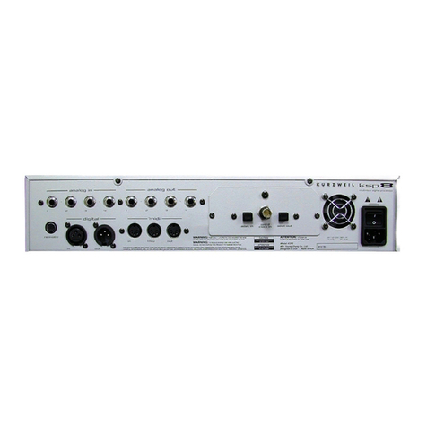
Data Translation DT9840 Series User manual

DT9840 Series
UM-19197-T
User’s Manual
Title Page

Seventeenth Edition
August, 2013
Data Translation, Inc.
100 Locke Drive
Marlboro, MA 01752-1192
(508) 481-3700
www.datatranslation.com
Fax: (508) 481-8620
E-mail: [email protected]
Copyright © 2013 by Data Translation, Inc.
All rights reserved.
Information furnished by Data Translation, Inc. is believed to be
accurate and reliable; however, no responsibility is assumed by
Data Translation, Inc. for its use; nor for any infringements of
patents or other rights of third parties which may result from its
use. No license is granted by implication or otherwise under any
patent rights of Data Translation, Inc.
Use, duplication, or disclosure by the United States Government
is subject to restrictions as set forth in subparagraph (c)(1)(ii) of
the Rights in Technical Data and Computer software clause at 48
C.F.R, 252.227-7013, or in subparagraph (c)(2) of the Commercial
Computer Software - Registered Rights clause at 48 C.F.R.,
52-227-19 as applicable. Data Translation, Inc., 100 Locke Drive,
Marlboro, MA 01752.
Data Translation® is a registered trademark of Data Translation,
Inc.
All other brand and product names are trademarks or registered
trademarks of their respective companies.
Copyright Page

Radio and Television Interference
This equipment has been tested and found to comply with CISPR EN55022 Class A and
EN61000-6-1 (CE) requirements and also with the limits for a Class A digital device, pursuant
to Part 15 of the FCC Rules. These limits are designed to provide reasonable protection against
harmful interference when the equipment is operated in a commercial environment. This
equipment generates, uses, and can radiate radio frequency energy and, if not installed and
used in accordance with the instruction manual, may cause harmful interference to radio
communications. Operation of this equipment in a residential area is likely to cause harmful
interference, in which case the user will be required to correct the interference at his own
expense.
Changes or modifications to this equipment not expressly approved by Data Translation
could void your authority to operate the equipment under Part 15 of the FCC Rules.
Note: This product was verified to meet FCC requirements under test conditions that
included use of shielded cables and connectors between system components. It is important
that you use shielded cables and connectors to reduce the possibility of causing interference
to radio, television, and other electronic devices.
Canadian Department of Communications Statement
This digital apparatus does not exceed the Class A limits for radio noise emissions from
digital apparatus set out in the Radio Interference Regulations of the Canadian Department of
Communications.
Le présent appareil numérique n’émet pas de bruits radioélectriques dépassant les limites
applicables aux appareils numériques de la class A prescrites dans le Règlement sur le
brouillage radioélectrique édicté par le Ministère des Communications du Canada.
FCC
Page


5
Table of Contents
About this Manual . . . . . . . . . . . . . . . . . . . . . . . . . . . . . . . . . . . . . . . . . . . . . . . . . . . . . . 9
Intended Audience. . . . . . . . . . . . . . . . . . . . . . . . . . . . . . . . . . . . . . . . . . . . . . . . . . . . . . . . . . . . . 9
How this Manual is Organized . . . . . . . . . . . . . . . . . . . . . . . . . . . . . . . . . . . . . . . . . . . . . . . . . . 9
Conventions Used in this Manual . . . . . . . . . . . . . . . . . . . . . . . . . . . . . . . . . . . . . . . . . . . . . . . . 9
Related Information . . . . . . . . . . . . . . . . . . . . . . . . . . . . . . . . . . . . . . . . . . . . . . . . . . . . . . . . . . . 10
Where to Get Help . . . . . . . . . . . . . . . . . . . . . . . . . . . . . . . . . . . . . . . . . . . . . . . . . . . . . . . . . . . . 10
Chapter 1: Principles of Operation . . . . . . . . . . . . . . . . . . . . . . . . . . . . . . . . . . . . . . . 11
System Features . . . . . . . . . . . . . . . . . . . . . . . . . . . . . . . . . . . . . . . . . . . . . . . . . . . . . . . . . . . . . . 14
Memory . . . . . . . . . . . . . . . . . . . . . . . . . . . . . . . . . . . . . . . . . . . . . . . . . . . . . . . . . . . . . . . . . 14
Clock Sources. . . . . . . . . . . . . . . . . . . . . . . . . . . . . . . . . . . . . . . . . . . . . . . . . . . . . . . . . . . . . 14
Internal Clock . . . . . . . . . . . . . . . . . . . . . . . . . . . . . . . . . . . . . . . . . . . . . . . . . . . . . . . . 15
DT9841, DT9841E, and DT9841-VIB Internal Clock . . . . . . . . . . . . . . . . . . . . . 15
DT9842/2 and DT9842/8 Internal Clock . . . . . . . . . . . . . . . . . . . . . . . . . . . . . . 15
External Clock . . . . . . . . . . . . . . . . . . . . . . . . . . . . . . . . . . . . . . . . . . . . . . . . . . . . . . . . 16
DT9841, DT9841E, and DT9841-VIB External Clock . . . . . . . . . . . . . . . . . . . . . 16
DT9842/2 and DT9842/8 External Clock . . . . . . . . . . . . . . . . . . . . . . . . . . . . . . 16
Scalable Bus Master Clock . . . . . . . . . . . . . . . . . . . . . . . . . . . . . . . . . . . . . . . . . . . . . 16
Operation Modes. . . . . . . . . . . . . . . . . . . . . . . . . . . . . . . . . . . . . . . . . . . . . . . . . . . . . . . . . . 17
Single-Value Operations . . . . . . . . . . . . . . . . . . . . . . . . . . . . . . . . . . . . . . . . . . . . . . . . 17
Single-Scan Operations . . . . . . . . . . . . . . . . . . . . . . . . . . . . . . . . . . . . . . . . . . . . . . . . 17
Multiple-Scan Input Operations . . . . . . . . . . . . . . . . . . . . . . . . . . . . . . . . . . . . . . . . . 18
Function Generator Output Operations . . . . . . . . . . . . . . . . . . . . . . . . . . . . . . . . . . 18
Continuous Loop Operations . . . . . . . . . . . . . . . . . . . . . . . . . . . . . . . . . . . . . . . . . . . 18
Scan Loop Operations . . . . . . . . . . . . . . . . . . . . . . . . . . . . . . . . . . . . . . . . . . . . . . 19
Block Loop Operations. . . . . . . . . . . . . . . . . . . . . . . . . . . . . . . . . . . . . . . . . . . . . . 19
List Loop Operations . . . . . . . . . . . . . . . . . . . . . . . . . . . . . . . . . . . . . . . . . . . . . . . 19
Triggers . . . . . . . . . . . . . . . . . . . . . . . . . . . . . . . . . . . . . . . . . . . . . . . . . . . . . . . . . . . . . . . . . . 20
Scalable Bus . . . . . . . . . . . . . . . . . . . . . . . . . . . . . . . . . . . . . . . . . . . . . . . . . . . . . . . . . . . . . . 21
LEDs . . . . . . . . . . . . . . . . . . . . . . . . . . . . . . . . . . . . . . . . . . . . . . . . . . . . . . . . . . . . . . . . . . . . 22
Analog Input Features. . . . . . . . . . . . . . . . . . . . . . . . . . . . . . . . . . . . . . . . . . . . . . . . . . . . . . . . . 23
Analog Input Channels . . . . . . . . . . . . . . . . . . . . . . . . . . . . . . . . . . . . . . . . . . . . . . . . . . . . 23
IEPE Functions. . . . . . . . . . . . . . . . . . . . . . . . . . . . . . . . . . . . . . . . . . . . . . . . . . . . . . . . . . . . 23
Input Resolution . . . . . . . . . . . . . . . . . . . . . . . . . . . . . . . . . . . . . . . . . . . . . . . . . . . . . . . . . . 24
Input Range and Gain . . . . . . . . . . . . . . . . . . . . . . . . . . . . . . . . . . . . . . . . . . . . . . . . . . . . . 24
Data Format . . . . . . . . . . . . . . . . . . . . . . . . . . . . . . . . . . . . . . . . . . . . . . . . . . . . . . . . . . . . . . 24
Data Transfer . . . . . . . . . . . . . . . . . . . . . . . . . . . . . . . . . . . . . . . . . . . . . . . . . . . . . . . . . . . . . 25
Error Conditions . . . . . . . . . . . . . . . . . . . . . . . . . . . . . . . . . . . . . . . . . . . . . . . . . . . . . . . . . . 25
Table of Contents

Contents
6
Analog Output Features . . . . . . . . . . . . . . . . . . . . . . . . . . . . . . . . . . . . . . . . . . . . . . . . . . . . . . . 26
Analog Output Channels . . . . . . . . . . . . . . . . . . . . . . . . . . . . . . . . . . . . . . . . . . . . . . . . . . . 26
Output Resolution. . . . . . . . . . . . . . . . . . . . . . . . . . . . . . . . . . . . . . . . . . . . . . . . . . . . . . . . . 26
Output Range and Gain . . . . . . . . . . . . . . . . . . . . . . . . . . . . . . . . . . . . . . . . . . . . . . . . . . . . 26
Output Filters. . . . . . . . . . . . . . . . . . . . . . . . . . . . . . . . . . . . . . . . . . . . . . . . . . . . . . . . . . . . . 27
Data Format . . . . . . . . . . . . . . . . . . . . . . . . . . . . . . . . . . . . . . . . . . . . . . . . . . . . . . . . . . . . . . 27
Data Transfer . . . . . . . . . . . . . . . . . . . . . . . . . . . . . . . . . . . . . . . . . . . . . . . . . . . . . . . . . . . . . 27
Error Conditions . . . . . . . . . . . . . . . . . . . . . . . . . . . . . . . . . . . . . . . . . . . . . . . . . . . . . . . . . . 28
Digital I/O Features. . . . . . . . . . . . . . . . . . . . . . . . . . . . . . . . . . . . . . . . . . . . . . . . . . . . . . . . . . . 29
Digital I/O Lines . . . . . . . . . . . . . . . . . . . . . . . . . . . . . . . . . . . . . . . . . . . . . . . . . . . . . . . . . . 29
Interrupt On Change . . . . . . . . . . . . . . . . . . . . . . . . . . . . . . . . . . . . . . . . . . . . . . . . . . . . . . 29
Counter/Timer Features . . . . . . . . . . . . . . . . . . . . . . . . . . . . . . . . . . . . . . . . . . . . . . . . . . . . . . . 30
C/T Channels . . . . . . . . . . . . . . . . . . . . . . . . . . . . . . . . . . . . . . . . . . . . . . . . . . . . . . . . . . . . 30
C/T Clock Sources . . . . . . . . . . . . . . . . . . . . . . . . . . . . . . . . . . . . . . . . . . . . . . . . . . . . . . . . 30
Internal C/T Clock . . . . . . . . . . . . . . . . . . . . . . . . . . . . . . . . . . . . . . . . . . . . . . . . . . . . 30
External C/T Clock . . . . . . . . . . . . . . . . . . . . . . . . . . . . . . . . . . . . . . . . . . . . . . . . . . . . 31
Internally Cascaded Clock . . . . . . . . . . . . . . . . . . . . . . . . . . . . . . . . . . . . . . . . . . . . . . 31
Gate Types . . . . . . . . . . . . . . . . . . . . . . . . . . . . . . . . . . . . . . . . . . . . . . . . . . . . . . . . . . . . . . . 32
Edge Types . . . . . . . . . . . . . . . . . . . . . . . . . . . . . . . . . . . . . . . . . . . . . . . . . . . . . . . . . . . . . . . 33
Pulse Output Parameters . . . . . . . . . . . . . . . . . . . . . . . . . . . . . . . . . . . . . . . . . . . . . . . . . . . 34
Polarity . . . . . . . . . . . . . . . . . . . . . . . . . . . . . . . . . . . . . . . . . . . . . . . . . . . . . . . . . . . . . . 34
Period Count . . . . . . . . . . . . . . . . . . . . . . . . . . . . . . . . . . . . . . . . . . . . . . . . . . . . . . . . . 35
Pulse Width Count . . . . . . . . . . . . . . . . . . . . . . . . . . . . . . . . . . . . . . . . . . . . . . . . . . . . 35
Counter/Timer Operation Modes . . . . . . . . . . . . . . . . . . . . . . . . . . . . . . . . . . . . . . . . . . . 36
Standard Counting . . . . . . . . . . . . . . . . . . . . . . . . . . . . . . . . . . . . . . . . . . . . . . . . . . . . 36
Measure . . . . . . . . . . . . . . . . . . . . . . . . . . . . . . . . . . . . . . . . . . . . . . . . . . . . . . . . . . . . . 38
Continuous Measure . . . . . . . . . . . . . . . . . . . . . . . . . . . . . . . . . . . . . . . . . . . . . . . . . . 39
Up/Down Counting . . . . . . . . . . . . . . . . . . . . . . . . . . . . . . . . . . . . . . . . . . . . . . . . . . . 41
One-Shot . . . . . . . . . . . . . . . . . . . . . . . . . . . . . . . . . . . . . . . . . . . . . . . . . . . . . . . . . . . . . 42
Repetitive One-Shot . . . . . . . . . . . . . . . . . . . . . . . . . . . . . . . . . . . . . . . . . . . . . . . . . . . 43
Chapter 2: Register Description. . . . . . . . . . . . . . . . . . . . . . . . . . . . . . . . . . . . . . . . . . 45
USB Bus/DSP Hardware Interface . . . . . . . . . . . . . . . . . . . . . . . . . . . . . . . . . . . . . . . . . . . . . . 47
Calibration and Setup . . . . . . . . . . . . . . . . . . . . . . . . . . . . . . . . . . . . . . . . . . . . . . . . . . . . . . . . . 51
Setting Up the Xicor Potentiometers . . . . . . . . . . . . . . . . . . . . . . . . . . . . . . . . . . . . . . . . . 52
Calibrating the Analog Input Subsystem . . . . . . . . . . . . . . . . . . . . . . . . . . . . . . . . . . . . . 54
Calibrating the Analog Output Subsystem . . . . . . . . . . . . . . . . . . . . . . . . . . . . . . . . . . . . 55
Analog Input Subsystem. . . . . . . . . . . . . . . . . . . . . . . . . . . . . . . . . . . . . . . . . . . . . . . . . . . . . . . 56
Analog Output Subsystem . . . . . . . . . . . . . . . . . . . . . . . . . . . . . . . . . . . . . . . . . . . . . . . . . . . . . 59
Digital I/O Subsystem. . . . . . . . . . . . . . . . . . . . . . . . . . . . . . . . . . . . . . . . . . . . . . . . . . . . . . . . . 61

Contents
7
Counter/Timer Subsystem . . . . . . . . . . . . . . . . . . . . . . . . . . . . . . . . . . . . . . . . . . . . . . . . . . . . . 62
Counter/Timer Operation Modes . . . . . . . . . . . . . . . . . . . . . . . . . . . . . . . . . . . . . . . . . . . 65
Count Sequence. . . . . . . . . . . . . . . . . . . . . . . . . . . . . . . . . . . . . . . . . . . . . . . . . . . . . . . . . . . 67
Event Counting Equations. . . . . . . . . . . . . . . . . . . . . . . . . . . . . . . . . . . . . . . . . . . . . . . . . . 67
Output Period/Frequency Equations . . . . . . . . . . . . . . . . . . . . . . . . . . . . . . . . . . . . . . . . 67
Output Pulse Width and Duty Cycle Equations. . . . . . . . . . . . . . . . . . . . . . . . . . . . . . . . 68
Counter Initialization . . . . . . . . . . . . . . . . . . . . . . . . . . . . . . . . . . . . . . . . . . . . . . . . . . . . . . 68
Memory . . . . . . . . . . . . . . . . . . . . . . . . . . . . . . . . . . . . . . . . . . . . . . . . . . . . . . . . . . . . . . . . . . . . . 70
Scalable Bus . . . . . . . . . . . . . . . . . . . . . . . . . . . . . . . . . . . . . . . . . . . . . . . . . . . . . . . . . . . . . . . . . 72
Chapter 3: Calibration . . . . . . . . . . . . . . . . . . . . . . . . . . . . . . . . . . . . . . . . . . . . . . . . . . 77
Using the DT9841 Calibration Utility . . . . . . . . . . . . . . . . . . . . . . . . . . . . . . . . . . . . . . . . . . . . 79
Calibrating the Analog Input Subsystem . . . . . . . . . . . . . . . . . . . . . . . . . . . . . . . . . . . . . . . . . 80
Connecting a Precision Voltage Source . . . . . . . . . . . . . . . . . . . . . . . . . . . . . . . . . . . . . . . 80
Using the Auto-Calibration Procedure . . . . . . . . . . . . . . . . . . . . . . . . . . . . . . . . . . . . . . . 80
Using the Manual Calibration Procedure . . . . . . . . . . . . . . . . . . . . . . . . . . . . . . . . . . . . . 81
Calibrating the Analog Output Subsystem . . . . . . . . . . . . . . . . . . . . . . . . . . . . . . . . . . . . . . . 82
Appendix A: Specifications . . . . . . . . . . . . . . . . . . . . . . . . . . . . . . . . . . . . . . . . . . . . . 83
Analog Input Specifications . . . . . . . . . . . . . . . . . . . . . . . . . . . . . . . . . . . . . . . . . . . . . . . . . . . . 84
Analog Output Specifications. . . . . . . . . . . . . . . . . . . . . . . . . . . . . . . . . . . . . . . . . . . . . . . . . . . 87
Digital Input Specifications. . . . . . . . . . . . . . . . . . . . . . . . . . . . . . . . . . . . . . . . . . . . . . . . . . . . . 88
Digital Output Specifications . . . . . . . . . . . . . . . . . . . . . . . . . . . . . . . . . . . . . . . . . . . . . . . . . . . 89
Counter/Timer Specifications . . . . . . . . . . . . . . . . . . . . . . . . . . . . . . . . . . . . . . . . . . . . . . . . . . 90
External Clock Specifications . . . . . . . . . . . . . . . . . . . . . . . . . . . . . . . . . . . . . . . . . . . . . . . . . . . 91
External Trigger Specifications. . . . . . . . . . . . . . . . . . . . . . . . . . . . . . . . . . . . . . . . . . . . . . . . . . 92
Power, Physical, and Environmental Specifications . . . . . . . . . . . . . . . . . . . . . . . . . . . . . . . . 93
Regulatory Specifications . . . . . . . . . . . . . . . . . . . . . . . . . . . . . . . . . . . . . . . . . . . . . . . . . . . . . . 94
Connector Specifications . . . . . . . . . . . . . . . . . . . . . . . . . . . . . . . . . . . . . . . . . . . . . . . . . . . . . . . 95
External Power Supply Specifications. . . . . . . . . . . . . . . . . . . . . . . . . . . . . . . . . . . . . . . . . . . . 97
Appendix B: Connector Pin Assignments . . . . . . . . . . . . . . . . . . . . . . . . . . . . . . . . . 99
DT9841, DT9842/2, and DT9842/8 Modules . . . . . . . . . . . . . . . . . . . . . . . . . . . . . . . . . . . . . 100
Connector J2 Pin Assignments . . . . . . . . . . . . . . . . . . . . . . . . . . . . . . . . . . . . . . . . . . . . . 101
Connector J3 Pin Assignments . . . . . . . . . . . . . . . . . . . . . . . . . . . . . . . . . . . . . . . . . . . . . 102
Connector J4 Pin Assignments . . . . . . . . . . . . . . . . . . . . . . . . . . . . . . . . . . . . . . . . . . . . . 102
Connector J6 Pin Assignments . . . . . . . . . . . . . . . . . . . . . . . . . . . . . . . . . . . . . . . . . . . . . 103
Connector J11 Pin Assignments . . . . . . . . . . . . . . . . . . . . . . . . . . . . . . . . . . . . . . . . . . . . 103
Connector J12 and J13 Pin Assignments . . . . . . . . . . . . . . . . . . . . . . . . . . . . . . . . . . . . . 104
Connector J17 Pin Assignments . . . . . . . . . . . . . . . . . . . . . . . . . . . . . . . . . . . . . . . . . . . . 105
Connector J18 Pin Assignments . . . . . . . . . . . . . . . . . . . . . . . . . . . . . . . . . . . . . . . . . . . . 106
Connector J19 Pin Assignments . . . . . . . . . . . . . . . . . . . . . . . . . . . . . . . . . . . . . . . . . . . . 107
Screw Terminal Block TB1 Assignments . . . . . . . . . . . . . . . . . . . . . . . . . . . . . . . . . . . . . 108

Contents
8
DT9841E Module . . . . . . . . . . . . . . . . . . . . . . . . . . . . . . . . . . . . . . . . . . . . . . . . . . . . . . . . . . . . 109
Connector J1 Pin Assignments . . . . . . . . . . . . . . . . . . . . . . . . . . . . . . . . . . . . . . . . . . . . . 110
Connector J2 Pin Assignments . . . . . . . . . . . . . . . . . . . . . . . . . . . . . . . . . . . . . . . . . . . . . 111
Connector J3 Pin Assignments . . . . . . . . . . . . . . . . . . . . . . . . . . . . . . . . . . . . . . . . . . . . . 113
Connector J4 Pin Assignments . . . . . . . . . . . . . . . . . . . . . . . . . . . . . . . . . . . . . . . . . . . . . 113
Connector J6 Pin Assignments . . . . . . . . . . . . . . . . . . . . . . . . . . . . . . . . . . . . . . . . . . . . . 114
Connector J11 Pin Assignments . . . . . . . . . . . . . . . . . . . . . . . . . . . . . . . . . . . . . . . . . . . . 114
Screw Terminal Block TB2 Assignments . . . . . . . . . . . . . . . . . . . . . . . . . . . . . . . . . . . . . 114
Screw Terminal Block TB3 Assignments . . . . . . . . . . . . . . . . . . . . . . . . . . . . . . . . . . . . . 115
Sleek Box Front Panel . . . . . . . . . . . . . . . . . . . . . . . . . . . . . . . . . . . . . . . . . . . . . . . . . . . . . . . . 116
Connector J1 Pin Assignments . . . . . . . . . . . . . . . . . . . . . . . . . . . . . . . . . . . . . . . . . . . . . 117
Connector J2 Pin Assignments . . . . . . . . . . . . . . . . . . . . . . . . . . . . . . . . . . . . . . . . . . . . . 118
Connector J19 Pin Assignments . . . . . . . . . . . . . . . . . . . . . . . . . . . . . . . . . . . . . . . . . . . . 119
EP358E Accessory Panel . . . . . . . . . . . . . . . . . . . . . . . . . . . . . . . . . . . . . . . . . . . . . . . . . . . . . . 120
Connector J202 Pin Assignments . . . . . . . . . . . . . . . . . . . . . . . . . . . . . . . . . . . . . . . . . . . 120
Connector J201 Pin Assignments . . . . . . . . . . . . . . . . . . . . . . . . . . . . . . . . . . . . . . . . . . . 122
Index . . . . . . . . . . . . . . . . . . . . . . . . . . . . . . . . . . . . . . . . . . . . . . . . . . . . . . . . . . . . . . . 125

9
About this Manual
This manual describes the hardware features of the DT9840 Series modules.
Intended Audience
This document is intended for engineers, scientists, technicians, or others responsible for
using and/or programming the DT9840 Series modules for data acquisition operations in the
Microsoft®Windows®XP, Windows Vista®, or Windows 7 operating system. It is assumed
that you have familiarity with data acquisition principles and that you understand your
application.
How this Manual is Organized
This manual provides detailed information about the operation of the DT9840 Series modules.
It is organized as follows:
•Chapter 1, “Principles of Operation,” describes the system features and the features of the
analog input, analog output, digital I/O, and counter/timer subsystems.
•Chapter 2, “Register Description,” describes all the registers that are used to program the
DT9840 Series modules.
•Chapter 3, “Calibration,” describes the DT9841 Calibration Utility.
•Appendix A, “Specifications,” lists the specifications of the module.
•Appendix B, “Connector Pin Assignments,” shows the pin assignments for the connectors
and the screw terminal assignments for the module.
• An index completes this manual.
Conventions Used in this Manual
The following conventions are used in this manual:
• Notes provide useful information or information that requires special emphasis, cautions
provide information to help you avoid losing data or damaging your equipment, and
warnings provide information to help you avoid catastrophic damage to yourself or your
equipment.
• Items that you select or type are shown in bold.

About this Manual
10
Related Information
Refer to the following documents for more information on using the DT9840 Series modules:
•Benefits of the Universal Serial Bus for Data Acquisition. This white paper describes why USB
is an attractive alternative for data acquisition. It is available on the Data Translation web
site (www.datatranslation.com).
•DT9840 Series Getting Started Manual (UM-19199). This manual, included on the DT9840
Series Software CD, describes the how to install the DT9840 Series modules and related
software.
•DT9840 Series DSP Library User’s Manual (UM-19591). This manual, included on the
DT9840 Series Software CD, describes how to write a DSP program for the DT9840 Series
modules.
•DT9840 Series Host Communication Library User’s Manual (UM-19593). This manual,
included on the DT9840 Series Software CD, describes how to write a host application
program that communicates with the DSP program running on the DT9840 Series
module.
• Documentation for Code Composer StudioTM Integrated Development Environment (IDE)
from Texas Instruments.
• Documentation for Texas Instruments TMS320C6713 DSP processor.
• Microsoft Windows XP, Windows Vista, or Windows 7 documentation.
• Microsoft Visual Studio documentation.
• USB 1.1 and USB 2.0 specifications on the USB web site (http://www.usb.org).
Where to Get Help
If you have difficulty using a DT9840 Series module, Data Translation’s Technical Support
Department is available to provide technical assistance.
To request technical support, go to our web site at http://www.datatranslation.com and click
on the Support link.
When requesting technical support, be prepared to provide the following information:
• Your product serial number
• The hardware/software product you need help on
• The version of the CD you are using
• Your contract number, if applicable
If you are located outside the USA, contact your local distributor; see our web site
(www.datatranslation.com) for the name and telephone number of your nearest distributor.

11
1
Principles of Operation
System Features . . . . . . . . . . . . . . . . . . . . . . . . . . . . . . . . . . . . . . . . . . . . . . . . . . . . . . . . . . . . . . 14
Analog Input Features . . . . . . . . . . . . . . . . . . . . . . . . . . . . . . . . . . . . . . . . . . . . . . . . . . . . . . . . . 23
Analog Output Features . . . . . . . . . . . . . . . . . . . . . . . . . . . . . . . . . . . . . . . . . . . . . . . . . . . . . . . 26
Digital I/O Features. . . . . . . . . . . . . . . . . . . . . . . . . . . . . . . . . . . . . . . . . . . . . . . . . . . . . . . . . . . 29
Counter/Timer Features . . . . . . . . . . . . . . . . . . . . . . . . . . . . . . . . . . . . . . . . . . . . . . . . . . . . . . . 30

Chapter 1
12
DT9840 Series modules provide simultaneous analog I/O, digital I/O, and counter/timer
operations on the USB bus. The hardware design features an embedded Texas Instruments
TMS320C6713 DSP processor that manages I/O functions on the module. This 300 MHz
processor provides float-point functionality and supports standard programming tools from
Texas Instruments, including Code Composer Studio.
Data Translation provides a library of DSP functions that you can use within a standard Code
Composer program to access the functionality of the DT9840 Series modules, as well a library
of communication functions that you can use to communicate between a DT9840 Series
module and a Windows-based host program. Refer to the DT9840 Series DSP Library User’s
Manual and DT9840 Series Host Communications Library User’s Manual for more information
about the functions included in these libraries. For maximum flexibility, you can also program
your own digital signal processing tasks at the DSP-level, if you wish.
Currently, the DT9840 Series consists of the DT9841, DT9841E, DT9841-VIB, DT9842/2, and
DT9842/8 modules. Table 1 describes the differences among the modules.
This chapter describes the operation of the DT9840 Series modules from a hardware
perspective. Figure 1 shows a block diagram of the DT9840 Series hardware architecture to
frame the discussion in this chapter. Note that bold entries indicate signals you can access.
For more detailed, register-level information, refer to Chapter 2 starting on page 45.
Table 1: DT9840 Series Modules
Models
Analog
Inputs
Converter
Type Resolution
Sampling
Rate
Analog
Filtering
Analog
Outputs
Scalable
Bus
DT9841 8DIa
a. DI refers to differential mode and SE refers to single-ended mode. For differential inputs only, you can configure the
termination resistance in software on a channel-by-channel basis.
Delta-Sigma 24-bitb
b. The input signal range is ±10 V.
200 Hz to
100 kHz
Ye s c
c. Software-selectable output filters of 5 kHz and 20 kHz are available.
2d
d. Software-selectable output ranges of ±10 V and ±2.5 V are available.
Ye s
DT9841-VIBe
e. The DT9841-VIB supports IEPE functions on the analog input channels. The DT9841-VIB module has two 8-bit digital
I/O ports, where the standard DT9841 product has three 8-bit digital I/O ports.
8SEaDelta-Sigma 24-bitb200 Hz to
100 kHz
Ye s c2dYe s
DT9841E 2DIaDelta-Sigma 24-bitb200 Hz to
100 kHz
Ye s c2dNo
DT9842/2 8SEaSuccessive
Approximation
16-bitb0 Hz to
100 kHz
No 2f
f. The output signal range is ±10 V.
Ye s
DT9842/8 8SEaSuccessive
Approximation
16-bitb0 Hz to
100 kHz
No 8fYe s

Principles of Operation
13
Figure 1: Block Diagram of the DT9840 Series Modules
USB Interface
Input FIFO
ID ROM
128 Kx8
SRAM
500 V Isolation Barrier
Isolated
DC to DC
Converter
External
+5 V Power
@ 6 A
HINT_L
16-Bit HPI
Address/
Data
4 Control
INT
Logic
Up to 24
Digital I/O
Lines and
3 Counter/
Timers
Programmable
Clock
External Clock
and Trigger
2 or 8
Analog
Inputs
2 or 8, 24-Bit
Delta-Sigma
or 8, 16-Bit Successive
Approximation A/Ds*
DSP
L2 Memory
256 KBytes
32 M x 32
SDRAM
2 or 8
DACs*
Reset
Rd_Wr_L
Isolation
Interface
16-Bit HPI
Address/Data
8 Ch
Data** A/D Clock
D/A Serial
Data
4 Control
INT 6 A/D Done
Reset
Rd_Wr_L
HINT_L
A/D and D/A
Data
JTAG
16-bit Scalable Bus 16-bit Scalable Bus
INT 4 (occurs
with A/D Trig, Ctr
Over, Dig
Change, SB
Done, or A/D or
D/A Error)
Serial Port
(1 - McBSP)
INT 5 D/A
Ready
INT 7 SB
FIFO
Control
Logic
* The DT9841 and DT9841-VIB features 8, 24-bit A/Ds and
2, 24-bit DACs.
The DT9841E features 2, 24-bit A/Ds and 2, 24-bit DACs.
The DT9842/2 features 8, 16-bit A/Ds and 2, 16-bit DACs.
The DT9842/8 features 8, 16-bit A/Ds and 8, 16-bit DACs.
**This is serial on the DT9841,
DT9841E, and DT9841-VIB, and parallel
on the DT9842/2 and DT9842/8.
1 M x 16
Flash RAM
The DT9841-VIB
has 16 digital I/O
lines.
FIFO

Chapter 1
14
System Features
The DT9840 Series modules provide the following system-level features:
• Memory, described below
• Clock sources, described on page 14
• Conversion modes, described on page 17
• Triggers, described on page 20
• Connections for multiple modules, described on page 21
• LEDs, described on page 22
Memory
All DT9840 Series modules provide 128 MB of onboard SDRAM and 2 MB of flash memory.
Flash memory is divided into two sections: a single 64 KB block is reserved for user data; the
remaining memory (2 MB – 64 KB) is reserved for storing a DSP program
You can download a program into SDRAM using the DT9840 Series Download Utility,
described in the DT9840 Series Getting Started Manual, and then run and debug the program.
Once you have debugged the program, you can store it in flash memory using the DT9840
Series Flash Download Utility, described in the DT9840 Series Getting Started Manual. This
allows the DSP program to run automatically each time the DT9840 Series module is powered
on, autonomously from the PC.
If desired, you can also copy a user data fie into flash memory using the DT9840 Series Flash
Download Utility. By copying a user data into flash, you can ensure that valuable information,
such as configuration information or collected data, persists across power cycles, even if the
DT9840 Series module loses power or is turned off.
Notes: Only one DSP program can be running on a module at one time. In addition, only one
user data file can be stored in flash memory at a time. However, you can overwrite the flash
memory up to one million times with a new or modified DSP program or data file, if you
wish.
Each DT9840 Series module also requires a CDB file for proper operation. Refer to the
DT9840 Series DSP Library User’s Manual for more information on CDB files.
Clock Sources
DT9840 Series modules support the following sample clock sources:
• Internal clock, described below
• External clock, described on page 16
• Scalable Bus master clock, described on page 16

Principles of Operation
15
Internal Clock
The internal clock has a 36 MHz time base for the DT9841, DT9841E, and DT9841-VIB
modules and an 18 MHz time base for the DT9842/2 and DT9842/8 modules. Conversions
start on a high-to-low transition after a rising edge of the internal calibration signal.
Use software to specify the internal clock source and the frequency at which to pace the input
and output operations and to start the sample clock. For the DT9841, DT9841E, and
DT9841-VIB, the sampling frequency ranges from 200 Hz to 100 kHz. For the DT9842/2 and
DT9842/8, the sampling frequency ranges from 0 Hz to 100 kHz.
Note: According to sampling theory (Nyquist Theorem), specify a frequency that is at least
twice as fast as the input’s highest frequency component. For example, to accurately sample a
20 kHz signal, specify a sampling frequency of at least 40 kHz to avoid aliasing.
The actual frequency that the module can achieve may be slightly different than the frequency
you specified due to the accuracy of the clock (0.01% for the DT9840 Series). You can
determine the actual clock frequency using software.
DT9841, DT9841E, and DT9841-VIB Internal Clock
On the DT9841, DT9841E, and DT9841-VIB modules, the value that you specify for the
internal clock frequency is multiplied by 512 internally to set the oscillator on the module. The
resulting signal from the oscillator is then divided by 2 to provide a clock signal to the A/D
and D/A converters that is oversampled 256 times and has a 50% duty cycle. For example, if
you specify an internal clock frequency of 100 kHz, internally the module sets the oscillator to
51.2 MHz then divides the resulting signal by 2 to provide a 25.6 MHz signal with a 50% duty
cycle to the A/D and D/A converters.
In addition, if you specify a sampling frequency between 200 Hz and 5 kHz, the DT9841,
DT9841E, and DT9841-VIB modules automatically filter the data using decimation and
interpolation filters. Refer to the DT9840 Series DSP Library User’s Manual for more
information on how these filters are implemented.
Once the sample clock is started, the DT9841, DT9841E, and DT9841-VIB modules require 37
clock pulses before the first conversion is completed (at 100 kHz, this delay is 370 μs).
Thereafter, the data is converted without delay (at 100 kHz, sampling occurs every 10 μs). This
initial delay is required by the filtering algorithms of the A/D and D/A converters.
DT9842/2 and DT9842/8 Internal Clock
Because the DT9842/2 and DT9842/8 use successive-approximation A/D converters and
provides no inherent filtering, no initial delay occurs (like on the DT9841, DT9841E, and
DT9841-VIB). Therefore, the converter always runs as fast as possible (at 100 kHz, sampling
occurs every 10 μs).
Internally, the DT9842/2 and DT9842/8 hardware divides the 18 MHz time base by a 32-bit
value to achieve the closest rate to the sampling rate you requested.

Chapter 1
16
External Clock
An external clock is useful when you want to pace acquisitions at rates not available with the
internal sample clock or when you want to synchronize a DT9840 Series module with other
devices in your system.
For the DT9841E module, connect the external clock to pin 23 of connector J1. For all other
modules, connect the external clock to the Ext Clk BNC input on the module. Use software to
specify the external clock source and to start the sample clock. Conversions start on a
high-to-low transition of the external clock signal after a rising edge of the internal calibration
signal.
DT9841, DT9841E, and DT9841-VIB External Clock
For the DT9841, DT9841E, and DT9841-VIB, ensure that the external clock source has a 50%
duty cycle. The resulting frequency of the external clock input is equal to the frequency of the
external clock signal that you connected to the module divided by 256 (this division is done
internally by the module), and must be in the range of 200 Hz to 100 kHz. For example, if you
need a sampling frequency of 100 kHz, use an external clock source with a frequency of
25.6 MHz.
Once the external clock is started, the DT9841, DT9841E, and DT9841-VIB modules require 37
clock pulses before the first conversion is completed (at 100 kHz, this delay is 370 μs).
Thereafter, the data is converted without delay (at 100 kHz, sampling occurs every 10 μs). This
initial delay is required by the filtering algorithms of the A/D and D/A converters.
DT9842/2 and DT9842/8 External Clock
Because the DT9842/2 and DT9842/8 use successive-approximation A/D converters and
provide no inherent filtering, no initial delay occurs (like on the DT9841, DT9841E, and
DT9841-VIB). Therefore, the resulting frequency of the external clock input is equal to the
frequency of the external clock signal that you connected to the module.
Scalable Bus Master Clock
Note: The Scalable Bus is not supported by DT9841E modules.
Use the Scalable Bus Master Clock source only if you are using the Scalable Bus to connect
multiple modules and you want to synchronize their operation. Refer to page 21 for more
information on Scalable Bus operations.
In this configuration, the clock, internal trigger, and reset signals are provided to the slave
modules from the master DT9840 Series module through the Scalable Bus. You can configure
the master module to use either an internal or external clock source. The Ext Clk BNC
connector on the slaves is not used.

Principles of Operation
17
Operation Modes
DT9840 Series modules support the following operation modes:
• Single value, described below
• Single scan, described on page 17
• Multiple scan input, described on page 18
• Function generator output, described on page 18
• Continuous loop operations (scan loop, block loop, and list loop), described on page 19
Single-Value Operations
Use software to perform a single-value operation. A DT9840 Series module acquires one value
from a specified channel or outputs one value to a specified channel on the next pulse of the
sample clock, and then stops. Triggers are ignored.
You can acquire data from an analog input channel, digital input line, or counter/timer
channel.
You can output data to either an analog output channel or a digital output line.
Single-Scan Operations
Use software to perform a single-scan operation. A DT9840 Series module acquires one input
scan record and/or outputs one output scan record on the next pulse of the sample clock, and
then stops. Triggers are ignored.
An input scan record consists of the following information:
• Eight analog input values corresponding to analog input channels 0, 1, 2, 3, 4, 5, 6, and 7.
For the DT9841, DT9841E, and DT9841-VIB, these are 24-bit values; for the DT9842, these
are 16-bit values.
Note: The DT9841E supports only two analog input channels (0 and 1). Therefore, values
for channels 2 through 7 in the input scan record should be ignored.
• One 24-bit value corresponding to all the digital input lines. For the DT9841-VIB, only
16-bits (ports 0 and 1) are accessible.
• One 32-bit value containing the state of the digital input lines. For the DT9841-VIB the
least significant 16-bits of this 32-bit value correspond to the digital inputs of port 0 and
port 1. On all other DT9840 Series modules, the least significant 24-bits of this 32-bit value
correspond to the digital inputs of port 0, port 1 and port 2.
• Three 32-bit values corresponding to counter/timer channels 0, 1, and 2.

Chapter 1
18
An output scan record consists of the following information:
• For the DT9841, DT9841E, and DT9841-VIB, two 24-bit values corresponding to analog
output channel 0 and 1. For the DT9842/2, two 16-bit values corresponding to analog
output channel 0 and 1. For the DT9842/8, eight 16-bit values corresponding to analog
output channels 0 to 7.
• One 24-bit value corresponding to all the digital output lines.
Multiple-Scan Input Operations
Use software to perform a multiple-scan input operation. When it detects a trigger event, the
DT9840 Series module acquires a specified number of input scan records, and then stops. An
input scan record is acquired on each pulse of the sample clock.; refer to page 17 for more
information on input scan records.
This is a synchronous operation; therefore, you cannot perform any other operation while this
operation is in process.
Function Generator Output Operations
Use software to start a function generator output operation. When it detects an initial trigger,
the DT9840 Series module outputs a buffer that contains a specified number of output scan
records. Refer to page 17 for more information on output scan records.
The module continuously outputs the data in the output scan records from the buffer in
memory to the analog output channels and/or digital output lines on each pulse of the sample
clock. Once the operation is started, the DSP is not used.
When you are finished outputting the data, use software to stop the operation.
Continuous Loop Operations
DT9840 Series modules support three types of continuous loop operations:
• Scan loop operations, described below
• Block loop operations, described on page 19
• List loop operations, described on page 19
The most appropriate mode depends on your application.
Use scan loop mode in control loops and other applications where you need to acquire a
sample on every tick of the sample clock and process the data as soon as possible. This mode
is less efficient than block loop and list loop operations, but allows more timely access to the
data.
Block and list loop operations process data in blocks. Your program gets called only when an
entire block of data has been acquired. These modes are more efficient than scan loop, but give
less frequent access to the incoming data.

Principles of Operation
19
Block and list loop operations are very similar in operation. The main difference is that block
loop uses only two block buffers, which are automatically allocated and managed, while list
loop uses a linked list of as many buffers as you want, but your program must allocate and
free each buffer appropriately.
Scan Loop Operations
Use software to start a scan loop operation. When it detects a trigger event, the module
continuously acquires an input scan record and/or outputs an output scan record on each
pulse of the sample clock, until you stop the operation. Refer to page 17 for more information
on input and output scan records.
The sample rate is determined by the frequency of the sample clock and is the rate at which a
single input scan record is acquired and a single output scan record is output; refer to page 14
for more information on the sample clock.
Block Loop Operations
Use software to start a block loop operation. When it detects a trigger event, the module
continuously acquires input blocks and/or outputs output blocks until you stop the
operation.
Each input block consists of the following information:
• Input scan records; refer to page 17 for more information on input scan records
• The number of scans in each block
• A flag that indicates whether or not the block is full
• A pointer to the next block
Each output block consists of the following information:
• Output scan records; refer to page 17 for more information on output scan records
• The number of scans in each block
• A flag that indicates whether or not the block is full
• A pointer to the next block
List Loop Operations
To perform a list loop operation, use software to allocate a linked list of input and/or output
blocks, and start the list loop operation. When it detects a trigger event, the module acquires
lists of input blocks and/or outputs lists of output blocks. Each list contains a specified
number of input and/or output blocks. Refer to page 19 for more information on input and
output blocks.
You can specify whether to stop the operation when the number of blocks have been filled (for
an input operation) or emptied (for an output operation) or whether to continue the operation
starting by overwriting the first block in the list.
When you are finished acquiring and/or outputting data, you can use software to stop a
continuous operation and free the previously allocated memory.

Chapter 1
20
Triggers
A trigger is an event that occurs based on a specified set of conditions. Using software, you
can specify these conditions by selecting one of the following trigger sources:
•Software trigger – The trigger event occurs immediately when you start the operation
(the computer issues a write to the module to begin conversions).
Note: If you are using the Scalable Bus to connect multiple modules and you want to use
an internal trigger to trigger the master and slave modules, no extra wiring is required.
The internal trigger signal is provided to the slave modules through the Scalable Bus
cables and connectors. Refer to page 21 for more information on using the Scalable Bus.
•External trigger – The trigger event occurs when the module detects a low to high
transition on the TTL-level signal connected to the external input of the module. For the
DT9841E module, connect the external trigger to pin 24 of connector J1. For all other
modules, connect the external trigger to the Ext Trig BNC on the module. This trigger
asserts EXT_INT4 for processing.
Note: If you are using the Scalable Bus to connect multiple modules and you want to
externally trigger the master and slave modules at the same time, you must supply an
external trigger signal to the master and each slave module using external wiring. The
external trigger signals is not provided through the Scalable Bus cable and connectors.
Refer to page 21 for more information on using the Scalable Bus.
When the DT9840 Series module detects the specified trigger event, the input and/or output
operation starts at the clock frequency of the specified clock source.
Figure 2 illustrates acquisition using an external trigger source. In this example, an input scan
record is acquired on each pulse of the selected clock source when the external trigger event
occurs.
Figure 2: Acquisition Using an External Trigger
The module detects a low-to-high transition on the
TTL-level signal attached to the Ext Trig BNC. Data
is acquired on each pulse of the sample clock.
Scan 1
Scan 2
Scan 3 Scan 4
Scan 5
Scan 6 Scan 7
Scan 8
Scan 9
Sample
Clock
This manual suits for next models
5
Table of contents
Popular Signal Processor manuals by other brands
West Mountain Radio
West Mountain Radio CLRstereo ClearSpeech operating manual
Euphonix
Euphonix DF64 Digital Frame manual
Radial Engineering
Radial Engineering JDI Duplex user guide
Extron electronics
Extron electronics FOX II RS 104 Setup guide
BSS Audio
BSS Audio Prosys PS-8810 user manual
CYP
CYP CPLUS-V11SE8 Operation manual
