Dimtel LLRF4.6 User manual

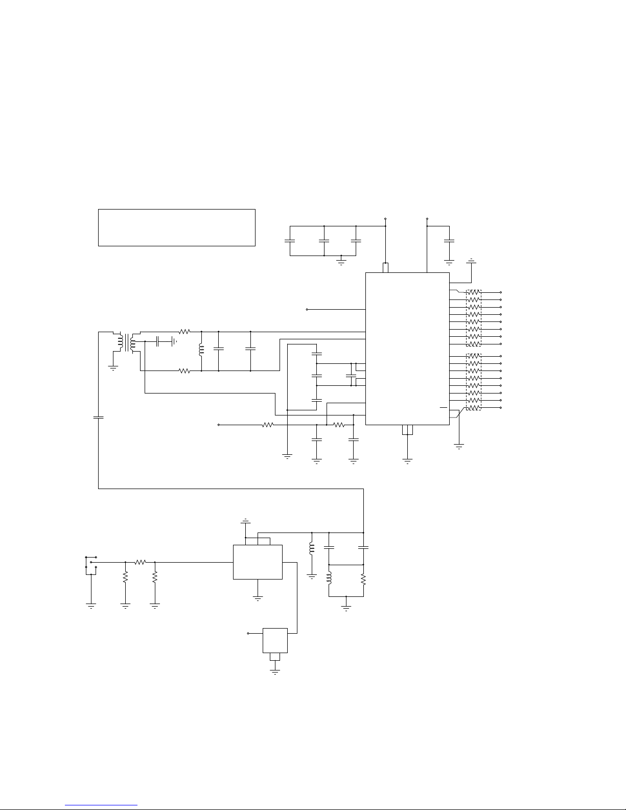
LLRF4.6 Evaluation Board
Dmitry Teytelman
July 7, 2014
Introduction
This document is an update of LLRF4 documentation packet, describing up-to-date in-
formation on 2013 LLRF4.6 revision of the board. The main difference between LLRF4
(last revision 4.2, dated 2009-06-28) and LLRF4.6 is the FPGA. The updated board uses
Spartan-6 FPGA in CS324 package. Normally, the boards are assembled with the largest
and fastest part fitting the footprint — XC6SLX45-3CSG324. While smaller parts can be
used, there is little rationale to do so.
Besides the component changes, several new or improved features have been incorporated:
•Transition from Spartan-3 XC3S1000 to Spartan-6 XC6SLX45;
•New FPGA core supply switcher capable of 2.5 A;
•Power supply jumpers replaced by zero ohm resistors;
•Maximally flat PCB backside for thermal pad mounting on cold plate;
•Reduced parasitics on RF/IF inputs
•High quality stripline LO distribution network, capable of 3 GHz;
•LO 1:8 splitter works to 3.4 GHz;
•LVDS signals routed as 100 Ω differential lines;
•LVDS termination resistors deleted;
•DS1822 thermometer in TO-92 replaced by DS18B20 in SO-8;
•Improved input channel shielding assembly.
The rest of this paper walks through these changes in detail.
FPGA
LLRF4.6 transitions to a more modern Xilinx FPGA. The part is also slightly faster
than the old Spartan-3. A short summary of differences between the two parts is shown
below. Of course, logic cells comparison is imprecise, since Spartan-6 uses new 6-input
LUT architecture. Xilinx uses some fudge factors to convert slice counts to vague “logic
cells”. XC3S1000 XC6SLX45 Notes
Logic cells 17280 43661
Multipliers 24 58 DSP48A1 in S6
BlockRAM 24 116 18kbits
One quirk of LLRF4.6 FPGA setup is that two data bits on high-speed DAC interface are
driven by dual function pins R15 (IO L1P CCLK 2) and V10 (IO L30N GCLK0 USERCCLK 2).
The bitfile must be generated with startup clock set to CCLK (-g StartUpClk:CClk
option of bitgen) for these pins to function as user outputs.
1

RF/LO Subsystem
At the RF input, parallel LC matching network was removed (never used on the original
LLRF4, layout considerations).
LO 1:8 power splitter (4 input mixers, 2 output mixers, power monitor, monitor connector)
is now built from 7 Mini-Circuits QCN-series quadrature splitters. These parts cover the
range from 220 MHz to 3.4 GHz in multiple bands.
The following parts can be used to populate the board according to the desired LO and
RF frequencies:
U13, U21, U22, U23, U24, U25, U26: 2-way LO splitter
220-470 MHz QCN-3+
330-580 MHz QCN-5+
425-675 MHz QCN-7+
450-750 MHz QCN-8+
800-1375 MHz QCN-12+
675-1300 MHz QCN-13D+
1100-1925 MHz QCN-19+
1350-2450 MHz QCN-25+
1700-2700 MHz QCN-27+
2500-3400 MHz QCN-34+
M1, M2, M101, M102, M103, M104: level 13 mixer
40-2500 MHz SYM-25DMHW
5-3000 MHz SYM-30DMHW
RF down- and up-conversion can also be bypassed during production.
2

IF filters
Many different IF filter designs have been developed for the original LLRF4. Most of
these should work well with LLRF4.6. Some have already been updated and tested on the
revised board — see the table below. CF is center frequency, BW is the bandwdith, level
refers to the bandwidth measurement level (drop in dB from the peak). For narrow filters,
3 dB measurement is appropriate, for wider ones, 1 and 0.5 dB bandwidth is specified. In
all cases, full bandwidth from lower to upper magnitude drop points is listed.
CF (MHz) BW (MHz) Level (dB) FS (dBm)
Tested on LLRF4.6
50 MHz (original) 48.5 9 3 11
39 MHz (Dimtel) 39 5.5 3 -4
74 MHz (Dimtel) 74 11 3 -3
81 MHz (Dimtel) 81 12.4 3 -3
Wideband (J-PARC) 34.1 68.1 0.5 6
Tested on LLRF4.2
110 MHz (FERMI) 110 58 3 -7
186 MHz (APEX) 190 28 0.5 -5
DAC outputs are also filtered on the board, with a simple two element filter. Original
configuration is 150 nH series inductor followed by 100 pF parallel capacitor. This setup
has low-pass response with roughly 41 MHz 3 dB bandwidth. This two element design can
be reconfigured for wider bandwidth, high-pass response, or bypassed altogether.
3

Power Supplies
FPGA 1.2 V core supply has been reconfigured on LLRF4.6. The new switching regulator
is based on the LTC3604 from Linear Technologies. Here is a comparison of the new device
with the MAX1820X used on LLRF4.2:
MAX1820X LTC3604 Units
Output current 0.6 2.5 A
Switching frequency 1 2 (up to 4) MHz
External sync Direct PLL
Sync frequency 10–16 (÷13) 0.8–4 MHz
The FPGA user I/O pin labeled ”SYNC” in the UCF provides the optional synchronization
function. Existing designs that used this feature based on the MAX1820X will need to be
adapted to the different characteristics of the new regulator chip.
One major problem with the MAX1820X was that changes in external sync drive cre-
ated large output voltage transients, locking up the FPGA (high power dissipation, no
JTAG/USB response). For those reasons, few designs made use of the synchronization
capability. With a synchronization PLL, LTC3604 can seamlessly go from free running
to synchronized mode and back to free running. Direct synchronization drive (without
divide-by-13 as in the MAX1820X) provides for more a flexible FPGA divide ratio.
Another power supply related change in LLRF4.6 is the deletion of 8 power output jumpers.
These made sense early on, but not at serial numbers above 100. Jumpers have been
replaced by zero ohm 0603 parts, so the regulators can still be disconnected from the
loads, if necessary.
4

LVDS inter-board communication
Since Spartan-6 supports internal differential termination for LVDS, on-board termination
resistors have been deleted. Direction and termination options can be specified in HDL
code now.
Unfortunately, Xilinx does not support bi-directional LVDS I/O with runtime termination
control. So the bit files have to explicitly define inputs and outputs, enabling termination
for the inputs. Since the signals are flipped on the cable, it is feasible to define 4 output
channels and 4 input channels, with identical bitfile on both FPGAs.
Connector Summary
Counterclockwise around the perimeter of the board
J101 SMA RF/IF input
J201 SMA RF/IF input
J301 SMA RF/IF input
J401 SMA RF/IF input
J15 SMA LO input (+26 dBm nominal)
J17 SMA Clock input (+1 dBm nominal)
J7 34-pin header Geek port (see schematic)
J18 SMA RF/IF output
J19 SMA RF/IF output
J20 SMA Analog output (0 to 2.5V, 2.2 kΩ)
J9 24-pin header 12 channels Analog output (0 to 2.5V)
J8 6-pin Weidmuller SNS-compatible interlock I/O
J21 LEMO Trigger
J22 LEMO Trigger
J6 2.1 mm +5V, 1.2A pseudo-regulated power input
J1 Type B USB
J3 20-pin 0.5mm flex LVDS inter-board communication
Interior test points
J23 U.Fl LO monitor (remove R809 to maintain match)
J24 U.Fl ICS83940D output 17
J25 U.Fl ICS83940D output 4
J26 U.Fl AD9512 output 3
J27 2mm IF output channel 2
J28 2mm IF output channel 1
2mm test points are intended for use with a high-impedance single-ended FET scope probe.
5

RF Input
VA
LO
CLK
PD
D0
D1
D2
D3
D4
D5
D6
D7
D8
D9
D10
D11
D12
D13
OVR
VD
VREF
RF Input
VA
LO
CLK
PD
D0
D1
D2
D3
D4
D5
D6
D7
D8
D9
D10
D11
D12
D13
OVR
VD
VREF
RF Input
VA
LO
CLK
PD
D0
D1
D2
D3
D4
D5
D6
D7
D8
D9
D10
D11
D12
D13
OVR
VD
VREF
RF Input
VA
LO
CLK
PD
D0
D1
D2
D3
D4
D5
D6
D7
D8
D9
D10
D11
D12
D13
OVR
VD
VREF
USB
interface
SLED
XERR
+3.3VD
DSPCLK
regulators
3.0V1
3.0V2
3.3VD
3.3VA
2.5VD
5Vin
3.3VA2
3.3V3
+1.2V
IMON
SYNC
VREF1
VREF2
IN1PD
IN1D0
IN1D1
IN1D2
IN1D3
IN1D4
IN1D5
IN1D6
IN1D7
IN1D8
IN1D9
IN1D10
IN1OVR
IN1D11
IN1D12
IN1D13
IN2PD
IN2D0
IN2D1
IN2D2
IN2D3
IN2D4
IN2D5
IN2D6
IN2D7
IN2D8
IN2D9
IN2D10
IN2OVR
IN2D11
IN2D12
IN2D13
IN3PD
IN3D0
IN3D1
IN3D2
IN3D3
IN3D4
IN3D5
IN3D6
IN3D7
IN3D8
IN3D9
IN3D10
IN3OVR
IN3D11
IN3D12
IN3D13
IN0PD
IN0D0
IN0D1
IN0D2
IN0D3
IN0D4
IN0D5
IN0D6
IN0D7
IN0D8
IN0D9
IN0D10
IN0OVR
IN0D11
IN0D12
IN0D13
fpga_caps
+3.3VD
+2.5VD
+1.2VD +1.2VD
+2.5VD
+3.3VD
SLED
XERR
SYNC
+5V
12
34
56
78
910
1112
13
14
1516
1718
1920
2122
2324
25
26
J7
27
29
31
28
30
32
33
34
J6
PJ102A
dual_rf_out
VD VA
QD0
QD1
QD2
QD3
QD4
QD5
QD6
QD7
QD8
QD9
QD10
QD11
QD12
QD13
LO1
ID0
ID1
ID2
ID3
ID4
ID5
ID6
ID7
ID8
ID9
ID10
ID11
ID12
ID13
SLEEP CLK
LO2
VREF
QD0
QD1
QD2
QD3
QD4
QD5
QD6
QD7
QD8
QD9
QD10
QD11
QD12
QD13
ID0
ID1
ID2
ID3
ID4
ID5
ID6
ID7
ID8
ID9
ID10
ID11
ID12
ID13
Local schematic pins at this level
an external database.
Clock
Distribution
Q0
Q1
Q2
Q3
Q4
Q5
Q6
Q7
Q8
Q9
Q10
Q11
(doubled) Qx2
Q13
Q14
Q15
Q16
Q17
CLKIN
3.3VA
SCLK
SDIO
CSB
housekeeping
ADC_CLK
ADC_SDO
ADC_SDI
ADC_CS
DAC_DIN2
DALLAS
LO
AO1
AO2
AI1
AI2
+3.3VD +3.3VA
+5V
DAC_CS
DAC_CLK
DAC_DIN1
IMON
DAC_DIN3
DALLAS
ADC_CLK
ADC_SDO
ADC_SDI
ADC_CS
J17
DAC_CLK
DAC_CS
DAC_DIN1
GEEK_DIO6
GEEK_PIN
GEEK_LED1
GEEK_LED3
GEEK_LED4
GEEK_LED2
GEEK_DIO1
GEEK_DIO2
GEEK_DIO3
GEEK_DIO4
GEEK_DIO5
GEEK_DIO6
are resolved to FPGA pads by
(5V)
RN7
IF_SLEEP
221Ω
R18
221Ω
R17
’1GT04
U10
221Ω
R19
10.0Ω
R20
0.47µF
C5
D4
150Ω
R25
D5
150Ω
R26
LOCAL_LED4
LOCAL_LED5
LO Dist
In
LO1
LO2
LO3
LO4
LO5
LO6
LO8
J15
J24
J25
IN OUT
GND
RN8
20dB
1
2
3
4
5
6
7
8
9
10
11
12
13
14
15
16
17
18
19
20
J3
Flex
L0P
L0N
L1P
L1N
L2P
L2N
L3P
L3N
L4P
L4N
L5P
L5N
L6P
L6N
L7P
L7N
J21
J22
TRIG2
332Ω
R38
TRIG1
332Ω
R39
TTL High turns on output
+3.3V+5V
Send_OK Got_OK
External Interlocks
N_SEND_OK N_GOT_OK
LBNL LLRF Digital Board V4.6
Larry Doolittle, LBNL Page 1/10
2013-08-13
Top Level
Dmitry Teytelman, Dimtel
DAC_DIN2
GEEK_DIO5
DIV_CSB
DAC_DIN3

681Ω
R107 681Ω
R106
1000pF
C105
1.0µF
C111
1.0µF
C110
+3.0VA +2.5VD
CLK
2.2µF
C112
PD
D0
D1
D2
D3
D4
D5
D6
D7
D8
D9
D10
OVR
Use 100Ωresistor pack
RN101
RN102
T101
150Ω
R103
ADT16-1T
10.0pF
C107
680nH
L103
330pF
C103
22nH
L102
D11
D12
D13
0.1µF
C109
2.2µF
C113
37.4Ω
R102
LO
150Ω
R101
1244 MHz
78 MHz
1300 MHz
+10 dBm F.S. +4 dBm
-2 dBm F.S.
+13 dBm
RF LO
IF
SYM-25DMHW
M101
LTC2249
D0
D1
D2
D3
D4
D5
D6
D7
D8
D9
D10
D11
OF
IN+
IN-
OE
SHDN
REFH
REFL
SENSE
VCM GND
CLK
+VSVDRVMODE
U101
(QFP32)
D12
D13
56 MHz
1.0 V F.S. diff. peak-peak
49.9Ω
R104
0.1µF
C114
0pF
C108
0pF
C104
470pF
C106
NPO
J101
INPUT
∞Ω
R109
681Ω
R108
VREF 0.625 V
10nH
L104
1.0µF
C117
LBNL LLRF Digital Board V4.6
Larry Doolittle, LBNL Page 2/10
2013-08-13
RF Input Channel
Dmitry Teytelman, Dimtel
IN OUT
GND
RN103
2dB
0.1µF
C116
0.1µF
C115
2.2µF
C118

0Ω
R1 0Ω
R2 RN1
M0
M1
TDO
TDI
TCK
TMS
U1
INIT_B
PROG_B
XC6SLX45-CS324
GCLK1
GCLK2
DONE
HSWAP_EN
GCLK0
FIFOADR0
CTL2
PA7
PA4
PA5
U2
CY7C68013A-LF56
PA3
PA2
PA1
PA0
SDA
SCL
XTALIN
XTALOUT
DPLUS
DMINUS
IFCLK
CLKOUT
RESET#
WAKEUP#
GND AGND
AVCCVCC
RESERVED
CTL2
PA6
Y1
24.0 MHz
12pF
C1
12pF
C2
SDA
SCL U3
WC
VCC E1
E2
E3
VSS
M24C32
4.75kΩ
R4 4.75kΩ
R5
1
2
3
4
5
6
USB
Type
B
J1T
332Ω
R6
D1
0Ω
R7
XERR
SLED
+3.3VD
+3.3VD +3.3VD
0.1µF
C81 0.47µF
C82 0.1µF
C83
+3.3VD
0Ω
R11
DSPCLK
’1GT04
U11
10.0Ω
R21
0.47µF
C6
+3.3VD
D2
150Ω
R22
’1GT04
U12
10.0Ω
R23
0.47µF
C7
+3.3VD
D3
150Ω
R24
LBNL LLRF Digital Board V4.6
Larry Doolittle, LBNL Page 3/10
2013-08-13
USB Interface
Dmitry Teytelman, Dimtel
0.47µF
C9
82.5kΩ
R34
0.47µF
C10
2.2µF
C622
4.75kΩ
R59
(48 MHz)
TP1
∞Ω
R60
∞Ω
R61
1
2
3
4
5
6
USB
Type
B
J1S
1MΩ
R63
4700pF
C86

+5V
22nH
L33
10nF
C602
EN VIN GND VOUT BYPASS
TPS79530
U601
tab
(NC)
3.0V1
10nF
C605
EN VIN GND VOUT BYPASS
TPS79530
U602
tab
(NC)
3.0V2
2.2µF
C603
2.2µF
C606
10nF
C608
EN VIN GND VOUT BYPASS
TPS79533
U603
tab
(NC)
3.3VA
2.2µF
C609
3.3VD
2.5VD
214 mA nominal
supplies 2 x ADC
214 mA nominal
supplies 2 x ADC
83 mA nominal
supplies DAC
213 mA nominal
supplies FPGA VCCO
140 mA nominal
supplies FPGA VCCAUX and ADC OVDD
10nF
C617
EN VIN GND VOUT BYPASS
TPS79533
U606
tab
(NC)
3.3VA3
2.2µF
C618
27 mA nominal
supplies System ADC and DAC
10nF
C620
EN VIN GND VOUT BYPASS
TPS79533
U607
tab
(NC)
3.3VA2
2.2µF
C621
146 mA nominal
supplies Clock Distribution
10nF
C614
EN VIN GND VOUT BYPASS
TPS79533
U605
tab
(NC)
2.2µF
C615
10nF
C611
EN VIN GND VOUT BYPASS
TPS79525
U604
tab
(NC)
2.2µF
C612
2.2µF
C601
2.2µF
C604
2.2µF
C607
2.2µF
C610
2.2µF
C613
2.2µF
C616
2.2µF
C619
0Ω
R602
0Ω
R604
0Ω
R606
0Ω
R608
0Ω
R610
0Ω
R612
0Ω
R614
Vin
RUN
PGOOD
TRACK/SS
BOOST
SW
Von
PGND
LTC3604EUD
U30
Vin
INTVcc
ITH
RT
SGND
MODE/SYNC
SW
FB
0.68µH
L31
47µF
C30
22pF
C34 +1.2V
22nH
L32
47nF
C33
22µF
C35
0.1uF
C36
SYNC
20kΩ
R31
20kΩ
R32
0.47Ω
R40
VIN+ VIN-
GND
V+ OUT
INA138
U5 IMON
2.2µF
C31
2.5 A max
supplies FPGA Core
1.0µF
C37 1.0µF
C38
VIN
GND
TP
NC
TP
NC
VOUT
TRIM
ADR421
U18
4.3kΩ
R41
4.3kΩ
R42
4.3kΩ
R43
4.3kΩ
R44
0.47µF
C39
100µF
C41
100µF
C40
VREF2
VREF1
LBNL LLRF Digital Board V4.6
Larry Doolittle, LBNL Page 4/10
2013-08-13
Voltage Regulators
Dmitry Teytelman, Dimtel
2.50 Volts
1.25 Volts
0.625 Volts
2.2µF
C29
10.0Ω
R33
0Ω
R37
D6
0Ω
R620
0Ω
R621
0Ω
R622
0Ω
R623
0Ω
R627
0Ω
R624
0Ω
R625
0Ω
R626
49.9Ω
R30
160kΩ
R50
2.2µF
C32
14kΩ
R62
150pF
C50
TP2

0.47µF
C63
+2.5VD
0.47µF
C64 0.47µF
C65 0.47µF
C66 0.47µF
C67 0.47µF
C68 0.47µF
C69 0.47µF
C70
0.47µF
C51
+1.2VD
0.47µF
C52
0.47µF
C53 0.47µF
C54
0.47µF
C71
0.47µF
C72
0.47µF
C73 0.47µF
C74
0.47µF
C58
+2.5VD
0.47µF
C59 0.47µF
C60 VCCO for banks 6, 7, 0, 1 connected to ADCs
0.47µF
C55
+3.3VD
0.47µF
C56
0.47µF
C57
0.47µF
C61 0.47µF
C62 VCCO for other banks
LBNL LLRF Digital Board V4.6
Larry Doolittle, LBNL Page 5/10
2013-08-13
FPGA Power Capacitors
Dmitry Teytelman, Dimtel
2.2µF
C623
2.2µF
C624

QD0
QD1
QD2
QD3
QD4
QD5
QD6
QD7
QD8
QD9
QD10
QD11
QD12
QD13
ID0
ID1
ID2
ID3
ID4
ID5
ID6
ID7
ID8
ID9
ID10
ID11
ID12
ID13
ISL5927 QOUTA
QOUTB
QCOMP
SLEEP
FSADJ
REFIO
REFLO
ICOMP
IOUTA
IOUTB
DVDD
DGND AGND
AVDD
CLK
U4
+3.3VD +3.3VA
0.1µF
C80
0.1µF
C79
0.1µF
C78 0.1µF
C76
0.1µF
C75
0.1µF
C77
2.00kΩ
R8
SLEEP
CLK
QD0
QD1
QD2
QD3
QD4
QD5
QD6
QD7
QD8
QD9
QD10
QD11
QD12
QD13
ID0
ID1
ID2
ID3
ID4
ID5
ID6
ID7
ID8
ID9
ID10
ID11
ID12
ID13
T1
T2
49.9Ω
R9
49.9Ω
R10
J19
J18
Full scale output current
is 32*Vref/R8
Internal Vref is 1.23 V
RF
LO
IF
SYM-25DMHW
M2
150nH
L3
100pF
C85
RF
LO
IF
SYM-25DMHW
M1
150nH
L2
100pF
C84
LO1
LO2
J27
J28
∞Ω
R45
0Ω
R46
VREF
LBNL LLRF Digital Board V4.6
Larry Doolittle, LBNL Page 6/10
2013-08-13
RF Output Channels
Dmitry Teytelman, Dimtel
IN OUT
GND
RN10
2dB
IN OUT
GND
RN9
2dB
ADT1-1WT
ADT1-1WT
0Ω
R35
2.2µF
C625

RN2
RN3
RN4
RN5
RN6
Q0
LVCMOS_CLK
CLK_SEL
PCLK
nPCLK
Q1
Q2
Q3
Q4
Q5
Q6
Q7
Q8
Q9
Q11
Q12
Q13
Q14
Q15
Q16
Q17
Q10
ICS83940D
VDDO
VDD
GND
U9
Q0
Q1
Q2
Q3
Q4
Q5
Q6
Q7
Q8
Q9
Q10
Q11
Q13
Q14
Q15
Q16
Q17
3.3VA
CLKIN
124Ω
R14
84.5Ω
R15
J26
4.12kΩ
R29
0.1µF
C46 0.1µF
C47 0.47µF
C48 0.47µF
C49
LBNL LLRF Digital Board V4.6
Larry Doolittle, LBNL Page 7/10
2013-08-13
Clock Distribution
Dmitry Teytelman, Dimtel
OUT0
OUT0B
OUT1
OUT1B
OUT2
OUT2B
OUT3
OUT3B
OUT4
OUT4B
STATUS
FUNCTION
DSYNC
DSYNCB
CLK1
CLK1B
CLK2
CLK2B
SCLK
SDIO
SDO
CSB
AD9512
VS
GND RSET
U17
1000pF
C3
1000pF
C4
200Ω
R16
CSB
SDIO
SCLK
124Ω
R12
84.5Ω
R13
T3
Mini-Circuits TCM4-19
DB714 case, gs pinout
1000pF
C8
Qx2
49.9Ω
R28 49.9Ω
R27
0.47µF
C42 0.47µF
C43 0.1µF
C44 0.47µF
C45
39.2kΩ
R36
2.2µF
C626
4.75kΩ
R58

ADC_CLK
ADC_SDO
ADC_SDI
ADC_CS
DAC_CLK
MCP3208
CH0
CH1
CH2
CH3
CH4
CH5
CH6
CH7
VDD
AGND
CLK
CS
DIN
DOUT
DGND
VREF
(SO-16)
U801
DAC_DIN1
DALLAS
DS1822
DQ
GND
(SOIC-8)
U804
VDD
+3.3VA
+3.3VA+3.3VA
AD8361
RFIN
PWDN
VPOS FLTR
VRMS
COMM
U805
(uSOIC-8) SREF
IREF
+3.3VA
1000pF
C802
49.9Ω
R801
2.21kΩ
R802
LO
Serial Number
ADC
3 x DAC
2.21kΩ
R803
10nF
C803
68.1Ω
R804
100pF
C804
10nF
C805
4.75kΩ
R805
+3.3VD
AO1
AO2
AI1
AI2
4.75kΩ
R806
4.75kΩ
R807
10nF
C806
221kΩ
R808
220pF
C807
+5V
30-2500 MHz from SMA
LBNL LLRF Digital Board V4.6
Larry Doolittle, LBNL Page 8/10
2013-08-13
Housekeeping
Dmitry Teytelman, Dimtel
NC
NC
DAC_CS
DAC_DIN2
22nH
L801
10nF
C808
IMON
J20
0Ω
R810
1
2
3
4
5
6
7
8
J9
9
10
11
12
13
14
15
16
17
18
19
20
21
22
23
24
AD56x4R
(MSOP-10)
U806
VDD
GND
VOUTA
SCLK
DIN
VOUTB
VOUTC
VOUTD
VREF
SYNC
AD56x4R
(MSOP-10)
U807
VDD
GND
VOUTA
SCLK
DIN
VOUTB
VOUTC
VOUTD
VREF
SYNC
AD56x4R
(MSOP-10)
U808
VDD
GND
VOUTA
SCLK
DIN
VOUTB
VOUTC
VOUTD
VREF
SYNC
DAC_DIN3
10nF
C810
10nF
C809
221Ω
R811
∞Ω
R812
∞Ω
R813
∞Ω
R814 221Ω
R815
0.47µF
C811
+3.3VA
0.47µF
C812 0.47µF
C813 0.47µF
C814 0.47µF
C815
+3.3VA
2.2µF
C627

MiniCircuits QCN
Sum
Term 0
90
U21
GND GND
LO1
LO2
LO3
LO4
LO5
LO6
LO8
LO
J23
49.9Ω
R809
LBNL LLRF Digital Board V4.6
Larry Doolittle, LBNL Page 9/10
2013-08-13
LO Distribution
Dmitry Teytelman, Dimtel
MiniCircuits QCN
Sum
Term 0
90
U22
GND GND
MiniCircuits QCN
Sum
Term 0
90
U23
GND GND
MiniCircuits QCN
Sum
Term 0
90
U24
GND GND
MiniCircuits QCN
Sum
Term 0
90
U26
GND GND
MiniCircuits QCN
Sum
Term 0
90
U13
GND GND
49.9Ω
R816
49.9Ω
R822
49.9Ω
R818
49.9Ω
R819
49.9Ω
R820
49.9Ω
R821
MiniCircuits QCN
Sum
Term 0
90
U25
GND GND
49.9Ω
R817

D701
RF_PERMIT
RF_PERMIT Return
IN+
IN-
Cathode VO
VE
VCC
Gnd
HCPL-060L
(SOIC-8)
U701
+3.3V
Low output means
Interlock OK
Send_OK
+5V
MPS_PERMIT
MPS_PERMIT Return
D702
J8
MMBD914
BZX384-C5V6
BCW60DCT
Got_OK
to FPGA Q701
Weidmuller P/N 172863
(WIED6)
(SOT23)
(SOT23)
(SOT23)
Rear
Panel
Mount
NPO
2.21kΩ
R705
221Ω
R704
82.5kΩ
R702
681Ω
R701
2.21kΩ
R703
47pF
C701
470pF
C702
LBNL LLRF Digital Board V4.6
Larry Doolittle, LBNL Page 10/10
2013-08-13
Interlock Input/Output
Dmitry Teytelman, Dimtel
681Ω
R706

llrf4.pcb
LLRF4, top, scale = 1:1.000

llrf4.pcb
LLRF4, bottom (mirrored), scale = 1:1.000

llrf4.pcb
LLRF4, topassembly, scale = 1:1.000

llrf4.pcb
LLRF4, bottomassembly (mirrored), scale = 1:1.000

llrf4.pcb
LLRF4, fab, scale = 1:1.000
Table of contents
Popular Motherboard manuals by other brands

Freetech
Freetech 586F63 user manual

Silicon Laboratories
Silicon Laboratories Si4827-DEMO user guide

Atmel
Atmel AT88CK440RED Getting started guide

mikroElektronika
mikroElektronika mikromedia for Stellaris M3 user guide

Intel
Intel D848PMB Product guide

Silicon Laboratories
Silicon Laboratories EFM8 Series Programming guide

Linear Technology
Linear Technology DC2043B Demo Manual

EVOC
EVOC EC7-1818CLD2NA user manual

Microchip Technology
Microchip Technology PIC32 Family user guide

P&E Microcomputer Systems
P&E Microcomputer Systems CYCLONE user manual

Infineon
Infineon EVAL-M1-IM818-A user manual

Biostar
Biostar H310MHD PRO manual