E-peas AEM10941 User manual
User guide AEM10941
User guide AEM10941
User guide AEM10941
Evaluation board for AEM10941
Description
The AEM10941 evaluation board is a printed circuit board
(PCB) featuring all the needed components to operate the
AEM10941 integrated circuit (IC). Please refer to the datasheet
for all the useful details about the AEM10941 (Document
DS AEM10941).
The AEM10941 evaluation board allows users to test the e-peas
IC and analyze its performances in a laboratory-like setting.
It allows easy connections to the energy harvester, the storage
element and the low-voltage and high-voltage loads. It also
provides all the configuration access to set the device in any
one of the modes described in the datasheet. The control and
status signals are available on standard pin headers, allowing
users to wire for any usage scenario and evaluate the relevant
performance.
The AEM10941 evaluation board is a plug and play, intuitive
and efficient tool for making the appropriate decisions (com-
ponent selection, operating modes) for the design of a highly
efficient solar energy powered subsystem in your target appli-
cation.
Applications
•PV cell harvesting •Home automation
•Industrial monitoring •E-health monitoring
•Geolocation •Wireless sensor nodes
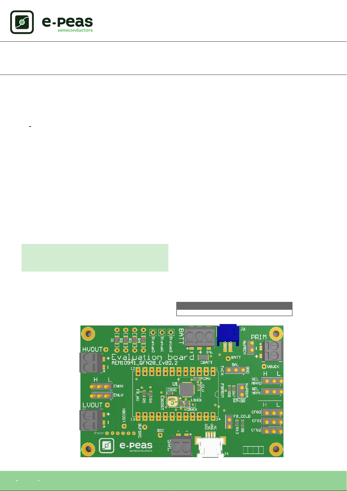
Appearance
Features
Four two-way screw terminals
- Source of energy (PV cell)
- Low-voltage load
- High-voltage load
- Primary energy storage element
One three-way screw terminal
- Energy storage element (battery or (super)capacitor)
One zero insertion force (ZIF) connector
- Alternative connection for the source
One 2-pin ”Shrouded Header”
- Alternative connection for the storage element
Eight 3-pin headers
- Maximum power point (MPP) configuration
- Low drop-out regulators (LDOs) enabling
- Energy storage elements and LDOs configuration
- Dual-cell supercapacitor configuration
Three 2-pin headers
- Primary battery configuration
- Cold-start configuration
Provision for ten resistors
- Custom mode configuration
- Cold start configuration
- Primary battery configuration
Three 1-pin headers
- Access to status pins
Device information
Part number Dimensions
2AAEM10941C0022 76 mm x 50 mm
1UG AEM10941 REV1.0 Copyright c
2018 e-peas SA 1UG AEM10941 REV1.0 Copyright c
2018 e-peas SA 1UG AEM10941 REV1.0 Copyright c
2018 e-peas SA

User guide AEM10941
User guide AEM10941
User guide AEM10941
Contents
1 Connections Diagram 3
1.1 Signals description . . . . . . . . . . . . . . . . . 4
2 General Considerations 5
2.1 Safety information . . . . . . . . . . . . . . . . . 5
2.2 Basic configurations . . . . . . . . . . . . . . . . 5
2.3 Advanced configurations . . . . . . . . . . . . . . 6
3 Functional Tests 7
3.1 Start-up . . . . . . . . . . . . . . . . . . . . . . 7
3.2 Shutdown . . . . . . . . . . . . . . . . . . . . . . 8
3.3 Switching on primary battery . . . . . . . . . . . 8
3.4 Cold start . . . . . . . . . . . . . . . . . . . . . . 8
3.5 Dual-cell supercapacitor balancing circuit . . . . . 9
4 Performance Tests 10
4.1 LDOs . . . . . . . . . . . . . . . . . . . . . . . . 10
4.2 BOOST efficiency . . . . . . . . . . . . . . . . . 10
4.3 Custom mode configuration . . . . . . . . . . . . 11
5 PV cell characterization 12
List of Figures
1 Connection diagram . . . . . . . . . . . . . . . . . 3
2STATUS[0] and HLDO evolution with BATT . . . . 7
3SRC and STATUS[2] while energy is extracted from
SRC (BATT under Vovch) . . . . . . . . . . . . . . 7
4 LDOs disabled around 600 ms after BATT reaches
Vovdis . . . . . . . . . . . . . . . . . . . . . . . . . 8
5 Switching from SRC to the primary battery . . . . . 8
6 AEM10941 behaviour during cold start . . . . . . . 9
7 HVOUT at 2.5V . . . . . . . . . . . . . . . . . . . 10
8 Boost efficiency for ISRC = 1 mA . . . . . . . . . . 11
9 PV cell first order model . . . . . . . . . . . . . . . 12
10 Typical I-V curve of a PV cell for high and low illu-
mination level . . . . . . . . . . . . . . . . . . . . . 12
11 Typical power-V curve of a PV cell for high and low
illumination level . . . . . . . . . . . . . . . . . . . 12
List of Tables
1 Pin description . . . . . . . . . . . . . . . . . . . . 4
2 Usage of CFG[2:0] . . . . . . . . . . . . . . . . . . 5
3 LDOs enabling . . . . . . . . . . . . . . . . . . . . 5
4 Usage of SELMPP[1:0] . . . . . . . . . . . . . . . . 5
2UG AEM10941 REV1.0 Copyright c
2018 e-peas SA 2UG AEM10941 REV1.0 Copyright c
2018 e-peas SA 2UG AEM10941 REV1.0 Copyright c
2018 e-peas SA

User guide AEM10941
User guide AEM10941
User guide AEM10941
1 Connections Diagram
Storage element
Mandatory connec
on
BAL (do
ed line) op
onal
If BAL pin is used, use a jumper to connect
«BAL» to «ToCN» or to «GND» if not used
See Sec
on 2.3.4
Source element
Leave
oa
ng if not used
Primary ba
ery
Mandatory connec
on
Connect a jumper to
each «NoPRIM» 2-pins
or connect the ba
ery
See Sec
on 2.3.2
High-voltage LDO output
Leave
oa
ng if not used
Low-voltage LDO output
Leave
oa
ng if not used
+
+
-
-
MPP con
gura
on
Mandatory connec
on
See Table 4
Ba
ery & LDOs
con
gura
on
Mandatory connec
on
See Table 2
LDOs enabling
Mandatory
connec
on
See Table 3
Cold-start
con
gura
on
Mandatory connec
on
Connect a jumper to
«FB_COLD» 2-pins or
use the resistors
See Sec
on 2.3.3
PV Cell + -
Warning
Please refer to Sec
on 2.1 before connec
ng the board
A 150 µF capacitor CBATT is already soldered on BATT
High voltage
load
Low voltage
load
Custom mode
con
gura
on
Leave
oa
ng if not used
See Sec
on 2.3.1
1
1
1
Figure 1: Connection diagram
3UG AEM10941 REV1.0 Copyright c
2018 e-peas SA 3UG AEM10941 REV1.0 Copyright c
2018 e-peas SA 3UG AEM10941 REV1.0 Copyright c
2018 e-peas SA

User guide AEM10941
User guide AEM10941
User guide AEM10941
1.1 Signals description
NAME FUNCTION CONNECTION
Power signals If used If not used
LVOUT Output of the low-voltage LDO regulator. Connect a load.
HVOUT Output of the high-voltage LDO regulator. Connect a load.
BAL Connection to mid-point of a dual-cell supercapac-
itor.
Connect mid-point
and jumper BAL to
”ToCN”.
Use a jumper to
connect ”BAL” to
”GND”.
BATT Connection to the energy storage element.
Connect storage ele-
ment in addition to
CBATT (150
µ
F).
Do not remove
CBATT.
PRIM Connection to the primary battery. Connect primary bat-
tery.
Connect a jumper to
each NoPRIM 2-pins.
SRC Connection to the harvested energy source. Connect the source
element. Leave floating.
Debug signals
VBOOST Output of the boost converter.
VBUCK Output of the buck converter.
BUFSRC Connection to an external capacitor buffering the
boost converter input.
Configuration signals
CFG[2]
CFG[1]
CFG[0]
SELMPP[1]
SELMPP[0]
FB PRIM Configuration of the primary battery. Use resistors R7-R8
(see Section 2.3.2).
Connect a jumper to
each NoPRIM 2-pins.
FB HV Configuration of the high-voltage LDO in the cus-
tom mode.
Use resistors R5-R6
(see Section 2.3.1). Leave floating.
FB COLD Configuration of the cold start. Use resistors R9-R10
(see Section 2.3.3).
Connect a jumper to
FB COLD 2-pins if
not used.
Configuration of the threshold voltages for the
energy storage element and the output voltage of
the LDOs.
Connect jumper
(see Table 2).
Cannot be left float-
ing (see Table 2).
Configuration of the MPP ratio. Connect jumper
(see Table 4).
Cannot be left float-
ing (see Table 4).
Control signals
ENHV Enabling pin for the high-voltage LDO. Connect jumper
(see Table 3).
Cannot be left float-
ing (see Table 3).
ENLV Enabling pin for the low-voltage LDO. Connect jumper
(see Table 3).
Cannot be left float-
ing (see Table 3).
Status signals
STATUS[2] Logic output. Asserted when the AEM performs
the MPP evaluation.
STATUS[1]
Logic output. Asserted if the battery voltage falls
under Vovdis or if the AEM is taking energy from
the primary battery.
STATUS[0] Logic output. Asserted when the LDOs can be
enabled.
Table 1: Pin description
4UG AEM10941 REV1.0 Copyright c
2018 e-peas SA 4UG AEM10941 REV1.0 Copyright c
2018 e-peas SA 4UG AEM10941 REV1.0 Copyright c
2018 e-peas SA
User guide AEM10941
User guide AEM10941
User guide AEM10941
2 General Considerations
2.1 Safety information
Always connect the elements in the following order:
1. Reset the board - see ”How to reset the AEM10941 evaluation board” on page 7.
2. Completely configure the PCB (jumpers/resistors);
-MPP configuration (SELMPP[0], SELMPP[1]) - see Table 4,
-Battery and LDOs configuration (CFG[0], CFG[1], CFG[2] and, if needed, R1-R2-R3-R4-R5-R6) - see Table 2,
-Primary battery configuration (NoPRIM or R7-R8) - see Section 2.3.2,
-LDOs enabling (ENHV and ENLV) - see Table 3,
-Cold-start configuration (FB COLD or R9-R10) - see Section 2.3.3,
-Balun circuit connection (BAL) - see Section 2.3.4.
3. Connect the storage elements on BATT and optionally the primary battery on PRIM.
4. Connect the high and/or low voltage loads on HVOUT/LVOUT (optional).
5. Connect the source element on SRC.
To avoid damage to the board, users are urged to follow this procedure.
2.2 Basic configurations
The MPP configuration is not available on the AEM10941 evaluation board. The MPP is by default configured to 50 %of
Voc as this ratio optimize the proposed rectifier efficiency.
Configuration pins Storage element threshold voltages LDOs output voltages Typical use
CFG[2] CFG[1] CFG[0] Vovch Vchrdy Vovdis Vhv Vlv
H H H 4.12 V 3.67 V 3.60 V 3.3 V 1.8 V Li-ion battery
H H L 4.12 V 4.04 V 3.60 V 3.3 V 1.8 V Solid state battery
H L H 4.12 V 3.67 V 3.01 V 2.5 V 1.8 V Li-ion/NiMH battery
H L L 2.70 V 2.30 V 2.20 V 1.8 V 1.2 V Single-cell (super) capac-
itor
L H H 4.50 V 3.67 V 2.80 V 2.5 V 1.8 V Dual-cell supercapacitor
L H L 4.50 V 3.92 V 3.60 V 3.3 V 1.8 V Dual-cell supercapacitor
L L H 3.63 V 3.10 V 2.80 V 2.5 V 1.8 V LiFePO4 battery
L L L Custom mode - see Section 2.3.1 1.8 V
Table 2: Usage of CFG[2:0]
ENLV ENHV LV output HV output
H H Enabled Enabled
H L Enabled Disabled
L H Disabled Enabled
L L Disabled Disabled
Table 3: LDOs enabling
SELMPP[1] SELMPP[0] Vmpp/Voc
L L 70%
L H 75%
H L 85%
H H 90%
Table 4: Usage of SELMPP[1:0]
5UG AEM10941 REV1.0 Copyright c
2018 e-peas SA 5UG AEM10941 REV1.0 Copyright c
2018 e-peas SA 5UG AEM10941 REV1.0 Copyright c
2018 e-peas SA

User guide AEM10941
User guide AEM10941
User guide AEM10941
2.3 Advanced configurations
A complete description of the system constraints and configu-
rations is available in Section 8 ”System configuration” of the
AEM10941 datasheet .
A reminder on how to compute the configuration resistors
value is provided below. Calculation can be made with the
help of the spreadsheet found at the e-peas website.
2.3.1 Custom mode
In addition to the pre-defined protection levels, the custom
mode allows users to define their own levels via resistors R1
to R4 and to tune the output of the high voltage LDO via
resistors R5-R6.
By defining RT = R1+R2+R3+R4 (1 MΩ≤RT ≤100 MΩ):
•R1 = RT (1 V / Vovch)
•R2 = RT (1 V / Vchrdy - 1 V / Vovch)
•R3 = RT (1 V / Vovdis - 1 V / Vchrdy)
•R4 = RT (1 - 1 V / Vovdis)
By defining RV = R5+R6 (1 MΩ≤RV ≤40 MΩ):
•R5 = RV (1 V / Vhv)
•R6 = RV (1 - 1 V / Vhv)
Make sure the protection levels satisfy the following conditions:
-Vchrdy + 0.05 V ≤Vovch ≤4.5 V
-Vovdis + 0.05 V ≤Vchrdy ≤Vovch - 0.05 V
- 2.2 V ≤Vovdis
-Vhv ≤Vovdis - 0.3 V
If unused, leave the resistor footprints (R1 to R6) empty.
2.3.2 Primary battery configuration
As to the main storage element, the primary battery protection
levels have to be defined. To do so, use resistors R7-R8.
By defining RP = R7+R8 (100 kΩ≤RP ≤500 kΩ):
•R7 = (Vprim min
4* RP) / 2.2 V
•R8 = RP - R7
If unused, connect a jumper to each ”NoPRIM” 2-pins.
2.3.3 Cold-start configuration
The cold-start voltage (i.e. the voltage needed at startup to
turn on the AEM10941) is by default at its minimum value
of 380 mV. This voltage can be tuned by the use of resistors
R9-R10.
By defining RC = R9+R10 (100 kΩ≤RC ≤10 MΩ):
•R9 = (0.38 V
Vcs * RC)
•R10 = RC - R9
If unused, connect a jumper to ”FB COLD” 2-pins.
2.3.4 Balun circuit configuration
When using a dual-cell supercapacitor (that does not already
include a balancing circuit), enable the balun circuit configu-
ration to ensure equal voltage on both cells. To do so:
- Connect the node between the two supercapacitor cells
to BAL (on BATT connector)
- Use a jumper to connect ”BAL” to ”ToCN”
If unused, use a jumper to connect ”BAL” to ”GND”.
6UG AEM10941 REV1.0 Copyright c
2018 e-peas SA 6UG AEM10941 REV1.0 Copyright c
2018 e-peas SA 6UG AEM10941 REV1.0 Copyright c
2018 e-peas SA
User guide AEM10941
User guide AEM10941
User guide AEM10941
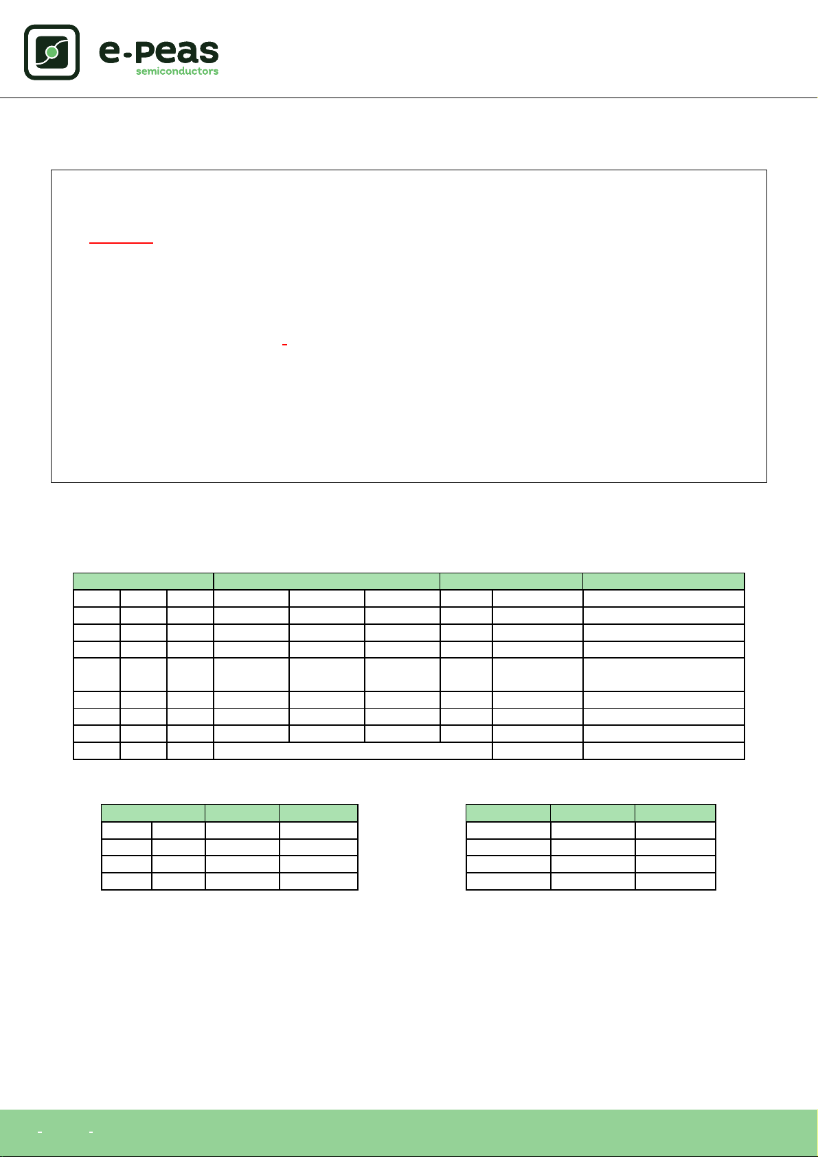
How to reset the AEM10941 evaluation board:
To reset the board, simply disconnect the storage device and the optional primary battery and connect the 6 ”Reset”
connections (working from the rightmost to the left) to a GND node (i.e. the negative pin of any connector) in order to
discharge the internal nodes of the system.
3 Functional Tests
This section presents a few simple tests that allow the user
to understand the functional behavior of the AEM10941. To
avoid damaging the board, follow the procedure found in Sec-
tion 2.1 ”Safety information”. If a test has to be restarted,
make sure to properly reset the system to obtain reproducible
results.
The following functional tests were made using the following
setup:
- Configuration: SELMPP[1:0] = LL, CFG[2:0] = HLL,
ENLV = H, ENHV = H
- Storage element: capacitor (4.7 mF + CBATT)
- Load: 10 kΩ on HVOUT,LVOUT floating
-SRC: current source (1 mA or 100
µ
A) with voltage com-
pliance (4 V)
Feel free to adapt the setup to match your system as long as
you respect the input and cold-start constraints (see Section
1 ”Introduction” of AEM10941 datasheet).
3.1 Start-up
The following example allows users to observe the behavior of
the AEM10941 in the wake-up mode.
Setup
1. Place the probes on the nodes to be observed.
2. Referring to Figure 1, follow steps 1 to 5 explained in
Section 2.1.
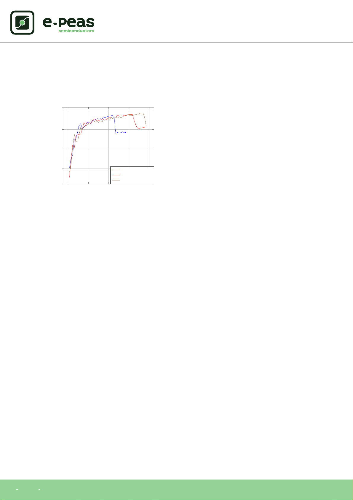
Observations and measurements
-BATT: Voltage rises as the power provided by the source
is transferred to the storage element (see Figure 2).
-SRC: Regulated at Vmpp, which is a voltage equal to the
open-circuit voltage (Voc) times the MPP ratio defined
in Table 4. Vsrc equals Voc during MPP evaluation (see
Figure 3). Note that Vsrc must be higher than 380 mV
to coldstart.
-HLDO/LLDO: Regulated when voltage on BATT first
rises above Vchrdy (see Figure 2).
-STATUS[0]: Asserted when the LDOs are ready to be
enabled (refer to Section 7.2 ”Normal mode” of the
AEM10941 datasheet) (see Figure 2).
-STATUS[2]: Asserted each time the AEM10941 per-
forms a MPP evaluation (see Figure 3).
0 5 10 15 20
0
1
2
Vchrdy
Time [s]
Voltage [V]
BATT STATUS[0]
HLDO
Figure 2: STATUS[0] and HLDO evolution with BATT
0 5 10 15 20
0
1
2
3
4
Vmpp
Voc
5s
Time [s]
Voltage [V]
STATUS[2] SRC
Figure 3: SRC and STATUS[2] while energy is ex-
tracted from SRC (BATT under Vovch)
7UG AEM10941 REV1.0 Copyright c
2018 e-peas SA 7UG AEM10941 REV1.0 Copyright c
2018 e-peas SA 7UG AEM10941 REV1.0 Copyright c
2018 e-peas SA

User guide AEM10941
User guide AEM10941
User guide AEM10941
3.2 Shutdown
This test allows users to observe the behavior of the
AEM10941 when the system is running out of energy.
Setup
1. Place the probes on the nodes to be observed.
2. Referring to Figure 1, follow steps 1 to 5 explained in
Section 2.1. Configure the board in the desired state
and start the system (see Section 3.1). Do not use a
primary battery.
3. Let the system reach a steady state (i.e. voltage on
BATT between Vchrdy and Vovch and STATUS[0] as-
serted).
4. Remove your source element and let the system dis-
charge through quiescent current and HVOUT/LVOUT
load(s).
Observations and measurements
-BATT: Voltage decreases as the system consumes the
power accumulated in the storage element. The voltage
remains stable after crossing Vovdis (see Figure 4).
-STATUS[0]: De-asserted when the LDOs are no longer
available as the storage element is running out of en-
ergy. This happens 600 ms after STATUS[1] assertion
(see Figure 4).
-STATUS[1]: Asserted for 600 ms when the storage ele-
ment voltage (BATT) falls below Vovdis (see Figure 4).
0 5 10 15 20
0
1
2
3
Vovdis
Time [s]
Voltage [V]
BATT STATUS[1] STATUS[0]
600ms
Figure 4: LDOs disabled around 600 ms after BATT
reaches Vovdis
3.3 Switching on primary battery
This example allows users to observe switching from the main
storage element to the primary battery when the system is
running out of energy.
Setup
1. Place the probes on the nodes to be observed.
2. Referring to Figure 1, follow steps 1 to 5 explained in
Section 2.1. Configure the board in the desired state and
start the system (see Section 3.1). Connect a primary
battery (example: 3.1 V coin cell with protection level
at 2.4 V, R7 = 68 kΩand R8 = 180 kΩ).
3. Let the system reach a steady state (i.e. voltage on
BATT between Vchrdy and Vovch and STATUS[0] as-
serted).
4. Remove your source element and let the system dis-
charge through quiescent current and HVOUT/LVOUT
load(s).
Observations and measurements
-BATT: Voltage decreases as the system consumes the
power accumulated in the storage element. The voltage
reaches Vovdis and then rises again to Vchrdy as it is
recharged from the primary battery (see Figure 5).
-STATUS[0]: Never de-asserted as the LDOs are still
functional (see Figure 5).
-HLDO: Stable and not affected by switching on the pri-
mary battery (see Figure 5).
0 5 10 15 20
0
1
2
3
Vovdis
Vchrdy
Time [s]
Voltage [V]
STATUS[0] BATT HLDO
Figure 5: Switching from SRC to the primary battery
3.4 Cold start
The following test allows users to observe the minimum volt-
age required to coldstart the AEM10941. Be careful to avoid
probing any unnecessary node to avoid leakage current induced
by the probe. Make sure to properly reset the board to observe
the cold-start behavior.
Setup
1. Place the probes on the nodes to be observed.
2. Referring Figure 1, follow steps 1 and 2 explained in
Section 2.1. Configure the board in the desired state.
Connect the jumper FB COLD. Do not plug any stor-
age element in addition to CBATT.
3. SRC: Connect your source element.
8UG AEM10941 REV1.0 Copyright c
2018 e-peas SA 8UG AEM10941 REV1.0 Copyright c
2018 e-peas SA 8UG AEM10941 REV1.0 Copyright c
2018 e-peas SA

User guide AEM10941
User guide AEM10941
User guide AEM10941
Observation and measurements
-SRC: Equal to the cold-start voltage during the cold-
start phase. Regulated at the selected MPPT percent-
age of Voc when cold start is over (see Figure 6). Be
careful that the cold-start phase time will shorten with
the input power. Limit it to ease the observation.
-BATT: Starts to charge when the cold-start phase is over
(see Figure 6).
0 1 2 3 4 5 6
0
0.25
0.5
0.75
1
Vcs
Time [s]
Voltage [V]
SRC BATT
Figure 6: AEM10941 behaviour during cold start
3.5 Dual-cell supercapacitor balancing circuit
This test allows users to observe the balancing circuit behavior
that maintains the voltage on BAL equilibrated.
Setup
1. Following steps 1 and 2 explained in Section 2.1 and re-
ferring to Figure 1, configure the board in the desired
state. Plug the jumper linking ”BAL” to ”ToCN”.
2. BATT: Plug capacitor C1 between the positive (+) and
the BAL pins and a capacitor C2 between BAL and the
negative (-) pins.
Select C1 6=C2 such that:
- C1 & C2 >1 mF
-C2∗Vchrdy
C1 ≥0.9 V
3. SRC: Plug your source element to start the flow of power
to the system.
Measurements
-BAL: Equal to half the voltage on BATT.
9UG AEM10941 REV1.0 Copyright c
2018 e-peas SA 9UG AEM10941 REV1.0 Copyright c
2018 e-peas SA 9UG AEM10941 REV1.0 Copyright c
2018 e-peas SA
User guide AEM10941
User guide AEM10941
User guide AEM10941
Warning regarding measurements:
Any item connected to the PCB (load, probe, storage device, etc.) involves a leakage current. This can negatively impact
the measurements. Whenever possible, disconnect unused items to limit this effect.
4 Performance Tests
This section presents the tests to reproduce the performance
graphs found in the AEM10941 datasheet and to understand
the functionalities of the AEM10941. To be able to reproduce
those tests, you will need the following:
- 1 voltage source
- 2 source measure units (SMUs)
- 1 oscilloscope
To avoid damaging the board, follow the procedure found in
Section 2.1 ”Safety information”. If a test has to be restarted,
make sure to properly reset the system to obtain reproducible
results (see ”How to reset the AEM10941 evaluation board”
on page 7).
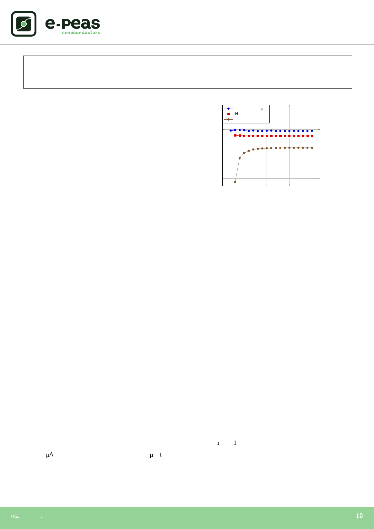
4.1 LDOs
The following example instructs users on how to measure the
output voltage stability of the LDOs (Figure 16 and Figure 17
of AEM10941 datasheet).
Setup
1. Referring to Figure 1, follow steps 1 and 2 explained in
Section 2.1. Configure the board in the desired state
and plug your storage element(s).
2. VBOOST: Connect SMU1. Configure it to source volt-
age with a current compliance of 200 mA.
3. HVOUT /LVOUT: Connect SMU2 to the LDO you want
to measure. Configure it to sink current with a voltage
compliance of 5 V for HVOUT or 2.5 V for LVOUT.
Manipulations
1. Impose a voltage between Vovch and 5 V on SMU1 to
force the AEM to start.
2. Sweep voltage on SMU1 from Vovdis + 50 mV to 4.5 V.
3. Repeat with different current levels on SMU2 (from
10
µ
A to 80 mA for HVOUT and from 10
µ
A to 20 mA
for LVOUT).
Measurements
-HVOUT/LVOUT: Measure the voltage.
3 3.5 4 4.5
2.3
2.4
2.5
2.6
VBOOST [V]
VHVOUT [V]
IHVOUT = 10
µ
A
IHVOUT = 10 mA
IHVOUT = 80 mA
Figure 7: HVOUT at 2.5V
4.2 BOOST efficiency
This test allows users to reproduce the efficiency graphs of the
boost converter (Figure 14 of AEM10941 datasheet).
Setup
1. Following steps 1 and 2 explained in Section 2.1 and re-
ferring to Figure 1, configure the board in the desired
state.
2. VBUCK: Connect a 2.3 V voltage source to prevent
VBUCK to sink from VBOOST.
3. SRC: Connect SMU1. Configure it to source current
with a voltage compliance of 0 V.
4. VBOOST: Connect SMU2. Configure it to source volt-
age with a current compliance of 200 mA.
5. STATUS[2]: Connect to one of the SMUs to detect
falling edge.
Manipulations
1. Impose a voltage between Vchrdy and 5 V on SMU2 to
force the AEM to start. When done, impose a voltage
between Vovdis + 50 mV and Vovch.
2. Sweep voltage compliance on SMU1 from 50 mV to 5 V.
3. Repeat with different current levels on SMU1 (from
100
µ
A to 100 mA) and with different voltage levels on
SMU2 (from Vovdis + 50 mV to Vovch).
Measurements
-STATUS[2]: Do not make any measurements while high
(boost converter is not active during MPP calculation).
-SRC: Measure the current and the voltage.
10UG AEM10941 REV1.0 Copyright c
2018 e-peas SA 10UG AEM10941 REV1.0 Copyright c
2018 e-peas SA 10UG AEM10941 REV1.0 Copyright c
2018 e-peas SA
User guide AEM10941
User guide AEM10941
User guide AEM10941
-VBOOST: Measure the current and the voltage. Repeat
the measurement a copious number of times to be sure
to capture the current peaks. Figure 8 has been ob-
tained by averaging over 100 measurements configured
with a 100 ms integration time.
- Deduce input and output power (P=U∗I) and effi-
ciency (η=P out/P in).
01234
40
60
80
100
VSRC [V]
Efficiency [%]
VBOOST = 2.6 V
VBOOST = 3.6 V
VBOOST = 4.1 V
Figure 8: Boost efficiency for ISRC = 1 mA
4.3 Custom mode configuration
This test allows users to measure the custom protection levels
of the storage element set by resistors R1 to R6.
Setup
1. Referring to Figure 1, follow steps 1 and 2 explained
in Section 2.1. Connect CFG[2:0] = LLL to select cus-
tom mode and choose R1 to R6 to configure the battery
protection levels and HVOUT output voltage.
2. Place the probes on the nodes to be observed.
3. SRC: Connect your source element to start the flow of
power to the system.
Manipulations
1. Remove the source element after the voltage on BATT
has reached steady state (between Vchrdy and Vovch).
Measurements
Measure the following nodes to ensure the correct behaviour
of the AEM10941 with respect to the custom configuration:
-STATUS[0]: Asserted when the LDOs can be enabled
(i.e. when BATT first rises above Vchrdy).
-STATUS[1]: Asserted when BATT falls below Vovdis.
-BATT: Rise up and oscillate around Vovch as long as
the source element has not been removed.
-HVOUT: Equal to the value set by R5-R6.
11UG AEM10941 REV1.0 Copyright c
2018 e-peas SA 11UG AEM10941 REV1.0 Copyright c
2018 e-peas SA 11UG AEM10941 REV1.0 Copyright c
2018 e-peas SA
User guide AEM10941
User guide AEM10941
User guide AEM10941
5 PV cell characterization
Isc
+
-
Voc
Figure 9: PV cell first order model
A photovoltaic cell can be modeled at first approximation by
a light-controlled current source in parallel with a diode as
illustrated in Figure 9. This allows to model the two main
characteristics of a PV cell: open-circuit voltage (Voc) and
short-circuit current (Isc).
The open-circuit voltage corresponds to the forward voltage
of the diode at no load while the short-circuit current is the
current delivered by the current source (i.e. when shorting the
+ and - terminals).
Voc Voc
Isc
Isc
Vout
Iout
High illumination Low illumination
Figure 10: Typical I-V curve of a PV cell for high and low
illumination level
Typical current vs voltage graph of a PV cell for different il-
lumination levels can be observed in Figure 10. Knowing that
P=I∗V, the associated power vs voltage curves can be
drawn as shown in Figure 11. For a given technology, the max-
imum extracted power is achieved at a voltage corresponding
to a given ratio of the open-circuit voltage (between 70% and
90%). This ratio is, in first approximation, independent of the
illumination level: as can be seen in Figure 11, Vmpp
Voc ≈Vmpp
Voc .
As presented in Table 4, the MPP configuration of the
AEM10941 allows you to select the voltage ratio that opti-
mizes the power extraction according to the characteristics of
your PV cell.
Vmpp
Vmpp VocVoc
Optimal power
Optimal power
Vout
Power
High illumination Low illumination
Figure 11: Typical power-V curve of a PV cell for high and
low illumination level
As can be seen in Figure 11, the power significantly decreases
with the voltage beyond the optimum Vmpp. It is then recom-
mended to configure the Vmpp/Voc ratio to be slightly lower
than the theoretical optimum and therefore avoid a significant
drop of performance.
12UG AEM10941 REV1.0 Copyright c
2018 e-peas SA 12UG AEM10941 REV1.0 Copyright c
2018 e-peas SA 12UG AEM10941 REV1.0 Copyright c
2018 e-peas SA
Other manuals for AEM10941
2
Table of contents
Other E-peas Motherboard manuals


