EIS TDGL004 User manual

Distributor of Microchip Technology: Excellent Integrated System Limited
Datasheet of TDGL004 - BOARD CEREBOT 32MX7 PIC32MX795
Excellent Integrated System Limited
Excellent Integrated System Limited
Stocking Distributor
Stocking Distributor
Click to view price, real time Inventory, Delivery & Lifecycle Information:
Click to view price, real time Inventory, Delivery & Lifecycle Information:
Microchip Technology
Microchip Technology
TDGL004
TDGL004
For any questions, you can email us directly:
For any questions, you can email us directly:
1 / 20
1 / 20
Distributor of Microchip Technology: Excellent Integrated System Limited
Datasheet of TDGL004 - BOARD CEREBOT 32MX7 PIC32MX795
C
Ce
er
re
eb
bo
ot
t
3
32
2M
MX
X7
7™
™
B
Bo
oa
ar
rd
d
R
R
e
e
f
f
e
e
r
r
e
e
n
n
c
c
e
e
M
M
a
a
n
n
u
u
a
a
l
l
Revision: October 20, 2011
Note: This document applies to REV C of the board. 1300 Henley Court | Pullman, WA 99163
(509) 334 6306 Voice and Fax
Doc: 502-186 page 1 of 19
Copyright Digilent, Inc. All rights reserved. Other product and company names mentioned may be trademarks of their respective owners.
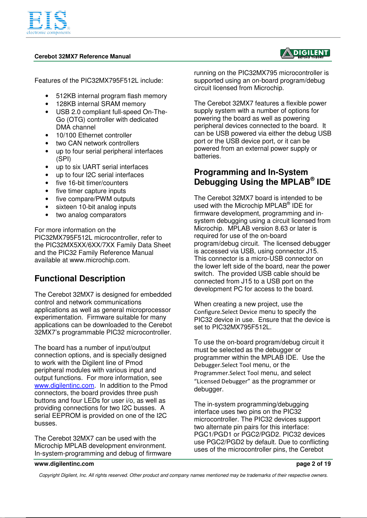
Overview
The Cerebot 32MX7 board is a useful tool for
embedded control and network
communications projects for both students and
hobbyists.
Its versatile design and programmable
microcontroller lets you access numerous
peripheral devices and program the board for
multiple uses. The board has many I/O
connectors and power supply options. It’s
network and communications features include
10/100 Ethernet interface, Full Speed USB 2.0
OTG interface, dual CAN network interfaces,
dual I2C buses, up to three UART ports and up
to three SPI ports.
The Cerebot 32MX7 works with the Microchip
MPLAB development environment and
provides built in programming and debugging
support within MPLAB.
The Cerebot 32MX7 provides a number of
connections for peripheral devices. It has six
connectors for attaching Digilent Pmod™
peripheral modules. Digilent Pmod peripheral
modules include H-bridges, analog-to-digital
and digital-to-analog converters, a speaker
amplifier, switches, buttons, LEDs, as well as
converters for easy connection to RS232,
screw terminals, BNC jacks, servo motors, and
more.
Features include:
•a PIC32MX795F512L microcontroller
•support for programming and
debugging within the Microchip MPLAB
development environment
•six Pmod connectors for Digilent
peripheral module boards
•10/100 Ethernet
•USB 2.0 Device, Host, and OTG
support
•two CAN network interfaces
•three push buttons
•four LEDs
•multiple power supply options, including
USB powered
•ESD protection and short circuit
protection for all I/O pins.
Cerebot 32MX7 Circuit Diagram
2 / 20
2 / 20
Distributor of Microchip Technology: Excellent Integrated System Limited
Datasheet of TDGL004 - BOARD CEREBOT 32MX7 PIC32MX795
Cerebot 32MX7 Reference Manual
www.digilentinc.com page 2 of 19
Copyright Digilent, Inc. All rights reserved. Other product and company names mentioned may be trademarks of their respective owners.
Features of the PIC32MX795F512L include:
•512KB internal program flash memory
•128KB internal SRAM memory
•USB 2.0 compliant full-speed On-The-
Go (OTG) controller with dedicated
DMA channel
•10/100 Ethernet controller
•two CAN network controllers
•up to four serial peripheral interfaces
(SPI)
•up to six UART serial interfaces
•up to four I2C serial interfaces
•five 16-bit timer/counters
•five timer capture inputs
•five compare/PWM outputs
•sixteen 10-bit analog inputs
•two analog comparators
For more information on the
PIC32MX795F512L microcontroller, refer to
the PIC32MX5XX/6XX/7XX Family Data Sheet
and the PIC32 Family Reference Manual
available at www.microchip.com.
Functional Description
The Cerebot 32MX7 is designed for embedded
control and network communications
applications as well as general microprocessor
experimentation. Firmware suitable for many
applications can be downloaded to the Cerebot
32MX7’s programmable PIC32 microcontroller.
The board has a number of input/output
connection options, and is specially designed
to work with the Digilent line of Pmod
peripheral modules with various input and
output functions. For more information, see
www.digilentinc.com. In addition to the Pmod
connectors, the board provides three push
buttons and four LEDs for user i/o, as well as
providing connections for two I2C busses. A
serial EEPROM is provided on one of the I2C
busses.
The Cerebot 32MX7 can be used with the
Microchip MPLAB development environment.
In-system-programming and debug of firmware
running on the PIC32MX795 microcontroller is
supported using an on-board program/debug
circuit licensed from Microchip.
The Cerebot 32MX7 features a flexible power
supply system with a number of options for
powering the board as well as powering
peripheral devices connected to the board. It
can be USB powered via either the debug USB
port or the USB device port, or it can be
powered from an external power supply or
batteries.
Programming and In-System
Debugging Using the MPLAB
®
IDE
The Cerebot 32MX7 board is intended to be
used with the Microchip MPLAB
®
IDE for
firmware development, programming and in-
system debugging using a circuit licensed from
Microchip. MPLAB version 8.63 or later is
required for use of the on-board
program/debug circuit. The licensed debugger
is accessed via USB, using connector J15.
This connector is a micro-USB connector on
the lower left side of the board, near the power
switch. The provided USB cable should be
connected from J15 to a USB port on the
development PC for access to the board.
When creating a new project, use the
Configure.Select Device menu to specify the
PIC32 device in use. Ensure that the device is
set to PIC32MX795F512L.
To use the on-board program/debug circuit it
must be selected as the debugger or
programmer within the MPLAB IDE. Use the
Debugger.Select Tool menu, or the
Programmer.Select Tool menu, and select
“Licensed Debugger” as the programmer or
debugger.
The in-system programming/debugging
interface uses two pins on the PIC32
microcontroller. The PIC32 devices support
two alternate pin pairs for this interface:
PGC1/PGD1 or PGC2/PGD2. PIC32 devices
use PGC2/PGD2 by default. Due to conflicting
uses of the microcontroller pins, the Cerebot
3 / 20
3 / 20

Distributor of Microchip Technology: Excellent Integrated System Limited
Datasheet of TDGL004 - BOARD CEREBOT 32MX7 PIC32MX795
Cerebot 32MX7 Reference Manual
www.digilentinc.com page 3 of 19
Copyright Digilent, Inc. All rights reserved. Other product and company names mentioned may be trademarks of their respective owners.
32MX7 is designed to use PGC1/PGD1.
Because of this, it is necessary to select the
use of PGC1/PGD1 for the debugging
interface. This is done using configuration
variables set using the
#pragma config
statement. The following statement must be
used to configure the microcontroller for use
with the on-board licensed debugger circuit:
#pragma config ICESEL = ICS_PGx1
The MPLAB IDE may report an error indicating
that the device is not configured for debugging
until a program containing this statement has
been programmed into the board.
Board Power Supply
Switch SW1, in the lower left corner of the
board is the power switch. Place this switch in
the ON position to turn on board power and in
the OFF position to turn off board power.
There are three power options for main power
to the board: USB powered from the debug
USB connector, USB powered from the USB
device connector, or external, non-USB
powered. Jumper block J16, (above the
Ethernet connector, J11) is used to select the
main power source. To select USB powered
from the debug connector, place the shorting
block in the DBG position. To select USB
power from the USB device connector, place
the shorting block in the USB position. This
option is used when the board is being used to
implement a bus powered USB device. To
power the board from an external power
supply, place the shorting block in the EXT
position. The board comes from the factor
jumpered for USB power from the debug USB
connector.
When powering the board from an external
power supply, there are two power supply
connectors that can be used: J17 and J18.
The barrel connector, J17, is used to power the
board from a “wall wart” style power supply.
This type of power supply is available from
many sources. Digilent has an optional power
supply available, the 5V Switching Power
Supply, that can be used with connector J17.
Connector J17 is a 2.5mm x 5.5mm coaxial
connector wired with the center terminal as the
positive voltage.
Connector J18 is a screw terminal connector
for an alternative power supply connection for
use with battery packs, bench supplies or other
power sources where use of a hard wired
power supply is desirable.
The Cerebot 32MX7 is rated for external power
from 3.6 to 5.5 volts DC. Using a voltage
outside this range will damage the board and
connected devices. For most purposes, when
using external power, a regulated 5V supply
should be used. When operating the board
from an external supply with a voltage less
than 5V, some features of the board won’t
work correctly.
When the Cerebot 32MX7 is operating as a
USB host, an external power supply connected
to either J17 or J18 must be used to power the
board. In addition to powering the logic on the
Cerebot 32MX7 board, this supply provides the
USB bus voltage supplied to any connected
USB device and must be a regulated 5V with
at least 500mA current capability to meet the
USB specifications.
The CAN bus operates at 5V, and therefore
the transceivers for the two CAN interfaces
require 5V to operate correctly and within the
CAN specification. When using the CAN
network interfaces, the board should be
operated from a 5V supply if using an external
power supply.
Connectors J17, and J18 are wired in parallel
and connect to the “External Power” position
(center position) on the Power Select jumper
block J16. A shorting block should be placed
on the “EXT” position of J16 when using this
option for board power. Only one of the
external power connectors should be used at a
time. If multiple power supplies are connected
simultaneously, damage to the board or the
power supplies may occur.
4 / 20
4 / 20

Distributor of Microchip Technology: Excellent Integrated System Limited
Datasheet of TDGL004 - BOARD CEREBOT 32MX7 PIC32MX795
Cerebot 32MX7 Reference Manual
www.digilentinc.com page 4 of 19
Copyright Digilent, Inc. All rights reserved. Other product and company names mentioned may be trademarks of their respective owners.
The power supply selected by the shorting
block on J16 will appear on the input power
supply bus, labeled VIN in the schematic. This
voltage is regulated to 3.3V to power the
debug circuit by IC11, a Microchip MCP1801
Low Dropout voltage regulator. This regulator
is turned on and the debug circuit is powered
whenever the power switch is in the on
position.
The USB specification requires that USB
devices not draw more than 100mA of current
until they have enumerated on the USB bus
and informed the host that they want to
consume more current. To meet this
specification, the debug circuit turns on main
board power by driving the PWR_ON signal
high after successfully enumerating on the
USB bus. The bus labeled on the schematic as
VCC5V0 is switched on when this occurs. The
VCC5V0 bus powers the input to the main
board voltage regulator, the input voltage to
the USB bus voltage load switch used when
using the board as a USB host, the power
supply voltage for the CAN transceivers, and
the 5V0 side of the power select jumpers for
the Pmod connectors. The voltage on the
VCC5V0 bus will be 5V when the board is
being operated from USB power or an external
regulated 5V supply. If a different external
supply voltage is used, that voltage will appear
on the VCC5V0 bus.
Note: The signal labeled DBG5V0 on the
schematic comes from the debug USB
connector. If the debug USB connector is not
connected to a live USB port, this voltage will
not be present and the debug circuit is not
involved in turning on board power. In this
case, the board power is turned on when the
power switch is placed in the ON position.
The PIC32 microcontroller and on-board I/O
devices operate at a supply voltage of 3.3V
provided by the VCC3V3 bus. The regulated
voltage on this bus is provided by a Microchip
MCP1726 Low Dropout voltage regulator,
IC10. This regulator is capable of providing a
maximum of 1A of current. The PIC32
microcontroller will use approximately 85mA
when running at 80MHz. The SMSC LAN8720
Ethernet PHY consumes approximately 45mA
when operating at 100Mbps. The Microchip
MCP2551 CAN transceivers can draw up to
75mA each when operating the CAN busses.
The other circuitry on the board will draw 10-20
mA. The remaining current is available to
provide power to attached Pmods and I
2
C
devices. The voltage regulator is on the
bottom of the board, approximately under the
“3” in the Cerebot 32MX7 logo, and will get
warm when the amount of current being used
is close to its limit.
The Cerebot 32MX7 can provide power to any
peripheral modules attached to the Pmod
connectors, JA-JF, and to I
2
C devices
powered from the I
2
C daisy chain connectors,
J7 and J8. Each Pmod connector provides
power pins that can be powered from either the
switched main power bus, VCC5V0, or
regulated voltage, VCC3V3, by setting the
voltage jumper block to the desired position.
The I
2
C power connectors only provide the
regulated voltage, VCC3V3.
USB Interface
The PIC32MX795 microcontroller contains a
USB 2.0 Compliant, Full Speed Device and
On-The-Go (OTG) controller. This controller
provides the following features:
•USB full speed host and device support
•Low speed host support
•USB OTG support
•Endpoint buffering anywhere in system
RAM
•Integrated DMA to access system RAM
and Flash memory.
The USB controller uses a phased lock loop,
PLL, to generate the necessary USB clock
frequency from the external primary oscillator
input frequency. By default, this PLL is
disabled. In order to use the USB controller, it
is necessary to enable the USB PLL, and set
the input divider to the correct value to
generate a valid USB clock. The input to the
USB PLL must be 4Mhz. The Cerebot 32MX7
provides an 8Mhz clock to the PIC32
5 / 20
5 / 20
Table of contents
Other EIS Motherboard manuals


