ELECRAFT KAT100 User manual
Elecraft
KAT100
Automatic Antenna Tuner
Revision D, February 13, 2015
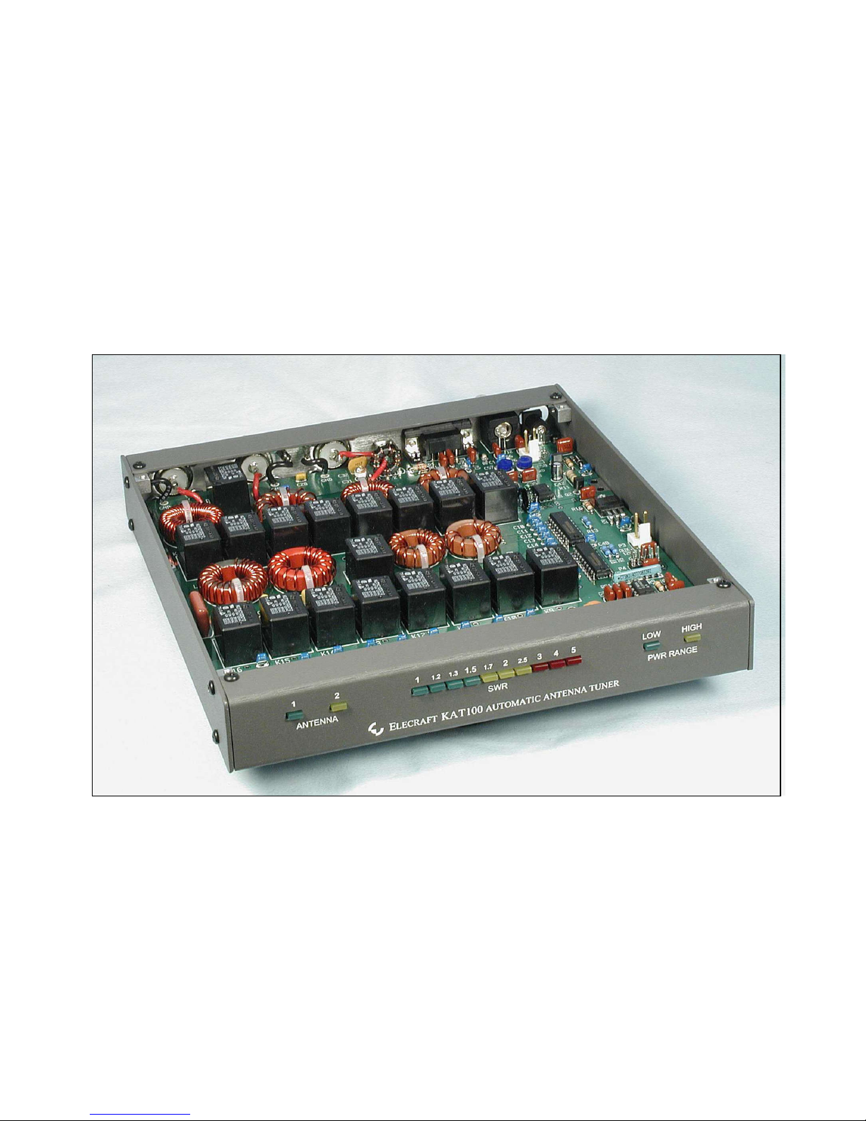
KAT100-1 shown above. See page 3 for photo of full-height version (KAT100-2).

2
Table of Contents
Introduction ................................................................................................................................................................................................................3
Parts Inventory...........................................................................................................................................................................................................4
RF Board Assembly .................................................................................................................................................................................................8
Front Panel Board Assembly................................................................................................................................................................................18
Final Assembly........................................................................................................................................................................................................19
Alignment and Test ................................................................................................................................................................................................ 7
Using the KAT100...................................................................................................................................................................................................31
Troubleshooting......................................................................................................................................................................................................34
Specifications..........................................................................................................................................................................................................36
Circuit Details..........................................................................................................................................................................................................37
Schematic ............................................................................................................................................................................................. APPENDIX A
Parts Placement Drawing..................................................................................................................................................................APPENDIX B

3
Introduction
The KAT100 automatic antenna tuner (ATU) is designed for use ith
the Elecraft K2/100 transceiver, as ell as the basic K2. It can match
loads ith SWRs in excess of 10:1, and can easily handle 150 atts of
transmit po er. Ten front-panel LEDs provide an accurate, real-time
SWR indication during transmit. The KAT100 also includes two
antenna jacks–the equivalent of t o auto-tuners connected to the rig.
Because of its tight integration ith the K2, the KAT100 offers many
advantages over generic external auto-tuners:
• Automatic po er reduction to 2 or 20 atts (in lo - and high-
po er modes) hen the K2's T U N E s itch is pressed; auto-tune is
possible ith as little as 0.2 atts in lo -po er mode
• Direct display of po er, SWR, and other data on the K2 LCD
• ATU can be configured using the K2 menu
• K2's POWER control setting indicated by t o LEDs
• K2's A N T 1 / 2 s itch selection indicated by t o LEDs
• L/C settings stored in EEPROM for both antennas on all bands
• SWR LEDs can use bar or dot mode (set by G R P H menu entry)
• All LEDs have t o brightness levels (set by L C D menu entry)
The ATU comes in t o enclosure styles, both of hich match the K2:
• The KAT100-1, sho n on the cover of this manual, is housed in a
lo -profile cabinet, intended to be placed beneath the K2. T o
anti-slip brackets are provided, so the K2 ill remain in position
even if the KAT100-1 is tilted up. (Also see Tilt-Stand Options
at right).
• The KAT100-2, sho n in the photo at right, is intended for side-
by-side arrangement ith the K2. It includes front and rear panels
that match our K2-sized EC2 enclosure kit. (The EC2 is sold
separately.) The EC2 cabinet provides plenty of room in the top
cover for your o n accessories.
Both KAT100 types are covered in this man al.
Tilt-Stand Options
T o different matching tilt stands are available, one for each KAT100
type. The E T S 2 is our standard, full-height tilt stand (2.5"), and is
recommended for use ith the KAT100-2. The E T S 1 5 is identical to
the ETS2 but is only 1.5" tall. It's ideal for use ith the lo -profile
KAT100-1, providing the optimum vie ing angle during operation.
Pre-Wound Toroids Available
The toroids in the KAT100 kit are not difficult to ind, and detailed
instructions are provided (beginning on page 13).
If you prefer not to ind the toroids yourself, you can obtain a full set
of pre- ound toroids ( ith leads stripped and tinned) from an Elecraft-
qualified source. Ordering information is at .elecraft.com.
You do not need to send your cores or wire to the winding service. You
can keep your set for replace ents or for use in your own projects.
KAT100-2

4
Parts Inventory
You should do a complete inventory, and if you find anything missing, contact Elecraft.
i
Leave painted panels rapped until they are needed during assembly. This ill protect the finish.
Items s pplied only with the KAT100-1 (with low-profile enclos re).
Pict re Ref. Designator(s) QTY Description Part #
MISC 1 KAT100-1 Front Panel E100138
MISC 1 KAT100-1 Rear Panel E100139
MISC 2 KAT100-1 Side Panel E100140
MISC 1 KAT100-1 Top Cover E100146
MISC 1 KAT100-1 Bottom Cover (note: includes holes for optional feet/tilt-stand) E100147
The items below are in a small bag labeled "Misc., KAT100-1" (p/n E850132)
HDWR 28 Scre , 4-40 x 3/16" Panhead Phillips, black (includes several spares) E700015
HDWR 8 2-D Fastener E100078
MISC 4 Rubber foot, self-adhesive E700024
MISC 2 Anti-slide bracket E100150
Items s pplied only with the KAT100-2 (for se with an EC2 enclos re).
Pict re Ref. Designator(s) QTY Description Part #
MISC 1 KAT100-2 Front Panel, EC2-compatible E100142
MISC 1 KAT100-2 Rear Panel, EC2-compatible E100143
The items below are in a small bag labeled "Misc., KAT100-2" (p/n E850136)
P3, P6 2 Connector, 2 pin male, 0.156"spacing (Aux 12V In and Aux RF Out) E620012
P 4 1 Connector, 10 pin (5x2) male, 0.1" spacing (Aux Control) E620040

5
Items in the KAT100 main parts bag (E850094), s pplied with both KAT100-1 and -2. Color codes and markings are sho n in parentheses.
Reference designators from 101 up refer to Front Panel components. Refer to Appendix A of the K2 o ner's manual for more parts photos.
i
Some components in this kit can be damaged by static discharge. Before handling diodes, transistors, and ICs, to ch a
gro nded, npainted metal s rface, or se a wrist strap gro nded thro gh a 1 megohm resistor.
Pict re Ref. Designator(s) QTY Description Part #
C1 1 Ca
p
acitor, 12
p
F, 2000V ceramic
(
3 KV ca
p
s ma
y
be substituted for an
y
2KV
)
E530107
C2 1 Capacitor, 22 pF 2000V ceramic E530108
C3 1 Capacitor, 39 pF 2000V ceramic E530109
C4 1 Capacitor, 82 pF 2000V ceramic E530110
C5,C6A,C6B,C7A-7D 7 Capacitor, 150 pF 2000V ceramic ("151") E530111
C8 1 Capacitor, 1200 pF, 1600V polypropylene film ("122") E530112
C32 1 Capacitor, 100 pF, 200V ("101") E530034
C33-36,C47 5 Capacitor, .001 µF, 50 V ("102") E530001
C37,C38,C39,C45,
C46 C50,C51,
7 Capacitor, .01 µF, 50 V ("103") E530009
C44,C49,C101,C102,
C56
5 Capacitor, .047 µF, 50V ("473") E530025
C9-30,C40,C41,C43,
C48,C52-55,C57-60
34 Capacitor, 0.1 µF, 50V ("104") E530020
C42 1 Capacitor, 10 µF, 35 V electrolytic E530045
C31 1 Capacitor, 5-30 pF trimmer E540001
D1,D2 2 Diode, 1N5711 (small glass body) E560004
D3,D4 2 Diode, 1N5817 (large black body) E560008
D110,D111,D112 3 Rectangular LED, Red (long lead is anode -- see text) E570007
D101,D103,D104,
D105,D106,D113
6 Rectangular LED, Green E570008
D102,D107,D108,
D109,D114
5 Rectangular LED, Yello E570009
E1 1 Scre terminal, right-angle PCB mount E700012

6
J1 1 Connector, DC barrel jack, 2.1mm, right-angle PCB mount E620026
J2 1 Connector, BNC, right-angle PCB mount, ith finishing nut and asher E850134
J3 1 Connector, DB9-F (female), right-angle PCB mount E620058
J4,J5,J6 3 Connector, SO239 E620064
J7 0 Connector, 6-pin female, 0.1" (not supplied; for future use) N/A
J101 1 Connector, 12-pin female, 0.1" spacing, PCB mount E620008
K1-K18 18 Relay, SPDT, 10A rating E640012
L1,L2,L3,L4 4 Toroidal inductor on T80-0 core (bro n, 0.8" dia.); see text E680020
L5,L6,L7,L8 4 Toroidal inductor on T94-2 core (red, 0.94" dia.); see text E680018
P1,P2 0 Connector, 2 pin male, 0.1" spacing (not supplied; for future use) N/A
P 5 1 Connector, 12 pin male, 0.1" spacing, right-angle mount E620065
Q1 1 Transistor, PNP, modified TO-92 package, Zetex ZTX789A
Note: Q1's labeling may be hard to read. The part number should be marked
on the silver-colored side.
E580019
Q2,Q3 2 Transistor, MOSFET, TO-92 package, 2N7000 E580002
Q101,Q102 2 Transistor, NPN, TO-92 package, PN2222 E580001
R5,R101-R114 15 Resistor, 120 ohms, 1/4W, 5% (brn-red-brn) E500022
R2 1 Resistor, 200 ohms, 1W, 5% (red-blk-brn) E500074
R115 1 Resistor, 220 ohms, 1/4W, 5% (red-red-brn) E500002
R116 1 Resistor, 470 ohms, 1/4W, 5% (yel-vio-brn) E500003
R11 1 Resistor, 680 ohm, 1/2 W, 5% (blue-gray-brn) E500085
K2 CTRL-R12 1 Resistor, 820 ohm, 1/4 W, 5% (gray-red-brn) E500001
R1,R8,R9 3 Resistor, 3.3K, 1/4W, 5% (org-org-red) E500017
R12,R16,R17,R18 4 Resistor, 10K, 1/4W, 5% (brn-blk-org) E500015
R3,R4 2 Potentiometer, 100K trimmer ("104") E520001
R6,R7,R13 3 Resistor, 8.45K, 1/4W, 1% (gray-yel-grn-brn) E500071
R15 0 Resistor (not supplied; for future use) N/A
RFC1 1 RF choke, 15µH (brn-grn-blk) NOTE: may be in bag with toroid cores E690012
RFC2 1 Toroidal inductor on FT37-43 core (gray, 0.37" dia.); see text E680003
RP1 1 Resistor pack, 3.9K, 4 individual resistors, 8 pins E510000
T 1 1 Transformer on FT50-43 toroidal core; see text E680008
U1 1 IC, Programmed microcontroller for KAT100, PIC16F877 or PIC16F877A E610012
U2,U3,U4,
U101,U102
5 IC, octal driver, TPIC6B595 E600032
U5 1 IC, op-amp, LM358 E600010
U6 1 IC, high-current op-amp, EL5146C E600041
U7 0 IC, EEPROM, 25LC320 (not supplied; reserved for future use) E600009
U8 1 IC, 5V regulator, TO-220 package, 78M05 or 7805 E600024
W1-W7 0 Wire jumper (leave open except as specified in text) N/A
Z1 1 Ceramic resonator, 4.0MHz, 0.2% tolerance (orange, ith 3 leads) E660001
7
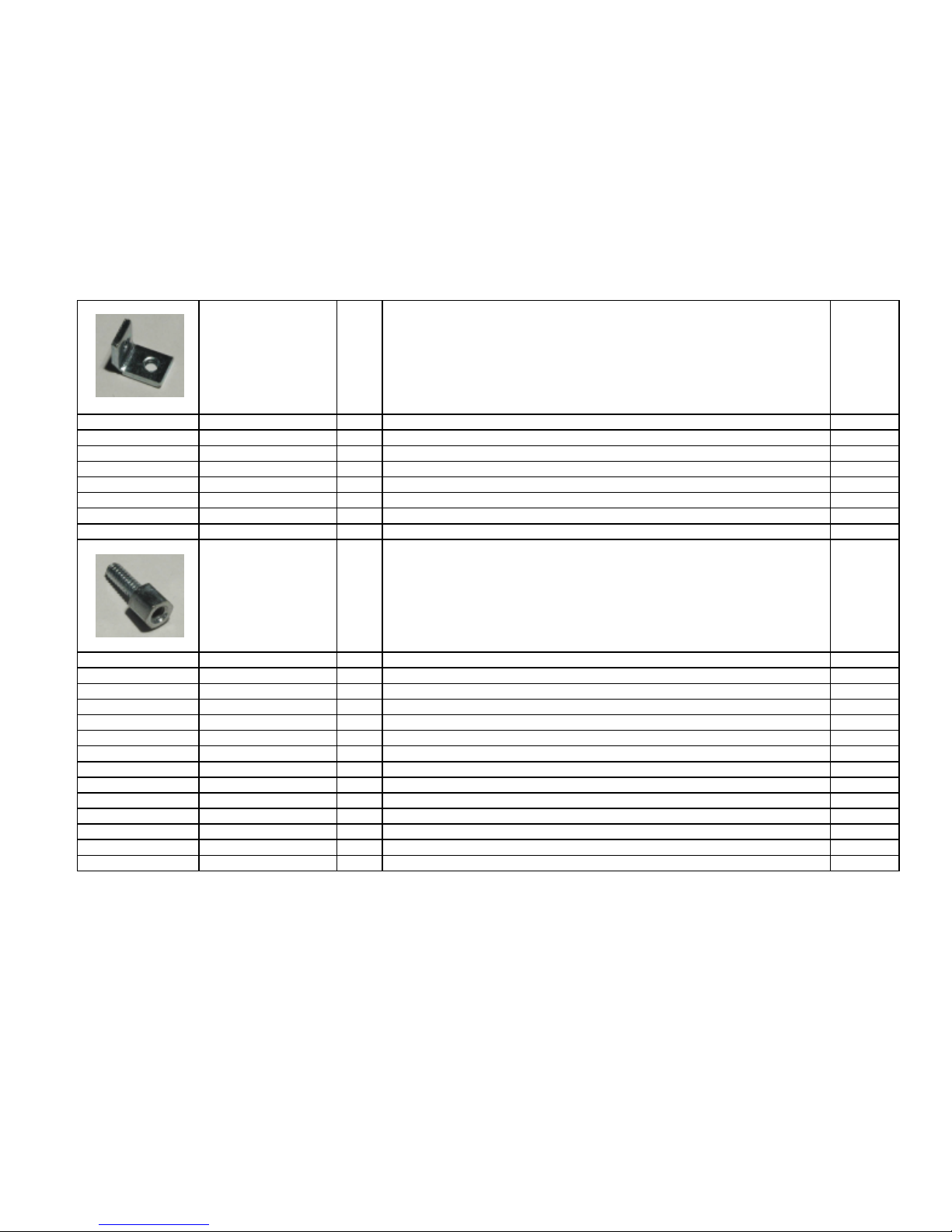
HDWR 2 L-bracket, front panel retainer, 4-40 threaded E700073
HDWR 14 Scre , 4-40 x 3/16" Panhead Phil, black (2 spares) E700015
HDWR 15 Scre , 4-40 x 5/16" Panhead Phil, zinc plated (2 spares) E700077
HDWR 1 Thumb scre , 6-32 x 1/2", ith black plastic knob E700070
HDWR 1 Nut, 6-32 E700069
HDWR 2 Flat asher, #6 E700067
HDWR 24 Split lock asher, #4 (2 spares) E700004
HDWR 15 Nut, 4-40 (2 spares) E700011
HDWR 3 Solder lug E700062
HDWR 2 Standoff, hex male-female (for DB9 connector, J3) E700078
MISC 1 Connector, 2.1 mm mating plug for J1 (DC barrel jack) E620032
MISC 1 Connector, 9-pin, DB9M (male), solder cup terminals (for control cable) E620049
MISC 3 ft. Cable, 4-conductor shielded E760009
MISC 1 DB9 backshell and hard are (for control cable) E620050
MISC 1 40-pin socket for U1 E620017
MISC 1 ft. Hookup ire, #20, black insulation E760006
MISC 1 ft. Hookup ire, #20, red insulation E760007
MISC 4 ft. #26 enamel ire for T1 and RFC2, red E760002
MISC 2 ft. #26 enamel ire for T1, green E760004
MISC 20 ft. #20 enamel ire for L1-L8, red E760022
MISC 10 Cable ties (for L1-L8; 2 spares) E980002
MISC 1 Sand paper E850090
MISC 1 KAT100 RF PC Board E100144
MISC 1 KAT100 Front Panel PC Board (may be rapped ith one of the panels) E100145
8
RF Board Assembly
Place the KAT100 RF PC board in front of you, ith the bottom
side up and the front edge facing you as sho n in the Parts
Placement Dra ing, Appendix B.
On the bottom of the board, along both edges, you'll find six
locations for 2-D fasteners. These are used to secure the RF board to
the chassis panels. In the next fe steps, just fo r 2-D fasteners ill be
attached, and the remaining t o locations ill not be used. Which four
locations to use depends on hether you're building a KAT100-1 or
KAT100-2:
KAT100-1: Use the t o 2-D locations near the front edge, and the
t o near the back edge.
KAT100-2: Use the t o 2-D locations near the front edge, and the
t o located about t o-thirds of the ay back. (The 2-D fasteners are
supplied ith the EC2 enclosure kit, not the KAT100-2.)
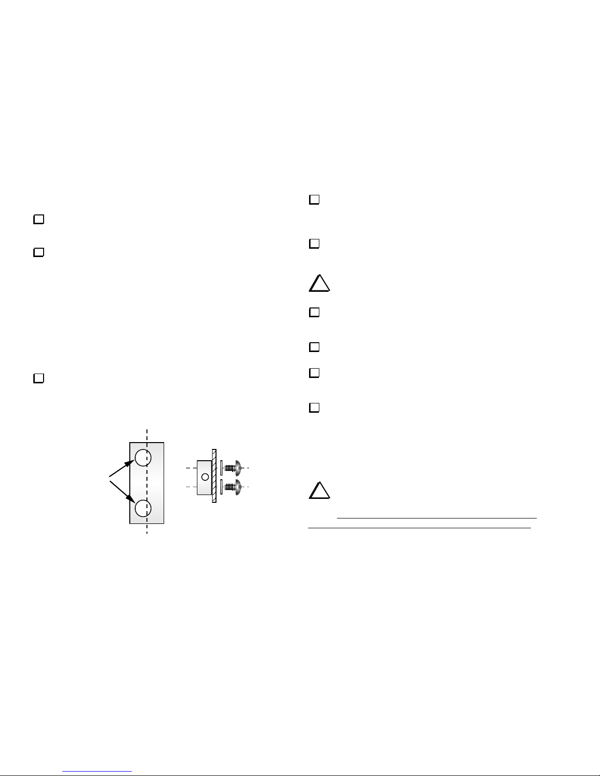
Locate a 2-D fastener and hold it vertically (Figure 1a). Looking
at a side ith t o holes, note that the holes are offset from the center.
The PC board outlines for the 2-D fasteners have a matching offset,
hich ill aid in installing them in the next step.
Holes offset
from center
(a) (b)
Fig re 1
Install 2-D fasteners at the four locations identified earlier, on the
botto of the RF board. Secure each fastener from the top side of the
board ith 3/16" (4.8 mm) pan-head scre s (black) and #4 split lock
ashers (Figure 1b).
Make sure the 2-D fasteners line up ith the edges of the PC
board and do not hang over. If they hang over or do not match their
component outlines, they are installed back ards.
i
The leads on small capacitors are fragile. Do not p ll on
the leads or bend them excessively.
Sort all capacitors into groups by physical appearance (size, color,
and lead spacing). Within these groups, sort them by capacitance
value.
Locate the component outline for capacitor C55, on the top side
of the board near the front edge.
Install a 0.1-µF capacitor (labeled "104") at C55. Keep the lead
length as short as possible. (If the leads are pre-formed, the capacitor
may sit slightly above the board.)
Bend C55's leads out ard on the opposite side of the board to
keep it from falling out or shifting position. Then solder the capacitor
and trim the leads.
Note: Components may be soldered one at a time or in groups. Leads
can be trimmed either before or after soldering. After soldering, trim
leads to about 1/16" [1.5 mm] or less in length.
i
If yo r solder joints are not clean and shiny, yo r iron
may not be hot eno gh, or yo may be sing the wrong type of
solder. These "cold" solder joints will likely res lt in poor
performance, reliability problems, or component fail re. Yo
may wish to cons lt o r web site for additional soldering
instr ctions and tool recommendations.

9
i
In the steps that follo , you'll be installing groups of
components. When orking from a long list, install all of the items on
one line before moving on to the next. Arro s (⇒) appear in the list
to remind you of this order. In general, assembly proceeds from left to
right and front to back across the board.
Install the capacitors listed belo . Start ith C29, hich is to the
left of C55, near relay K16. Check each capacitor's labeling
caref lly (shown in parentheses).
__ C29, 0.1 (104) ⇒__ C26, 0.1 (104) ⇒__ C25, 0.1 (104)
__ C24, 0.1 (104) __ C23, 0.1 (104) __ C22, 0.1 (104)
__ C21, 0.1 (104) __ C20, 0.1 (104) __ C19, 0.1 (104)
__ C60, 0.1 (104)
__ C51, .01 (103) __ C50, .01 (103) __ C39, .01 (103)
__ C40, 0.1 (104) __ C38, .01 (103) __ C46, .01 (103)
__ C37, .01 (103) __ C48, 0.1 (104) __ C43, 0.1 (104)
__ C9, 0.1 (104) __ C18, 0.1 (104) __ C17, 0.1 (104)
__ C16, 0.1 (104) __ C15, 0.1 (104) __ C14, 0.1 (104)
__ C13, 0.1 (104) __ C12, 0.1 (104) __ C11, 0.1 (104)
__ C10, 0.1 (104) __ C52, 0.1 (104) __ C53, 0.1 (104)
__ C45, .01 (103) __ C54, 0.1 (104) __ C36, .001 (102)
__ C35, .001 (102) __ C41, 0.1 (104) __ C58, 0.1 (104)
__ C44, .047 (473) __ C49, .047 (473) __ C56, .047 (473)
__ C57, 0.1 (104) __ C47, .001 (102) __ C59, 0.1 (104)
__ C33, .001 (102) __ C34, .001 (102)
__ C32, 100 pF, 200V (101)
__ C28, 0.1 (104) __ C30, 0.1 (104)
__ C27, 0.1 (104) Near K17, middle of board
Install the high-voltage capacitors listed belo .
Note: Save a fe of the clipped leads from these capacitors for use as
ground jumpers in later steps.
__ C1, 12 (12) ⇒__ C2, 22 (22) ⇒__ C3, 39 (39)
__ C4, 82 (82) __ C5, 150 (151) __ C6B, 150 (151)
__ C6A, 150 (151) __ C7D, 150 (151) __ C7C, 150 (151)
__ C7B, 150 (151) __ C7A, 150 (151)
__ C8, 1200 pF (122)
Install the electrolytic capacitor, C42 (10 µF), near the back-right
corner of the board. The (+) lead must be installed in the hole marked
ith a "+". The (+) lead is usually longer than the (–) lead, and the (–)
lead is identified by a black or hite stripe.
Install the 5 to 30 pF ceramic trimmer capacitor, C31, near the
back edge of the board. Orient the flat side of the trimmer as indicated.
Using a small flat-blade scre driver, set the trimmer to its
midpoint (scre driver slot perpendicular to the flat side).
Sort all of the resistors by value. The color bands on 1% resistors
( hich usually have a blue body) can be difficult to read, so you should
use a DMM (digital multimeter) to verify their values. Tape them to a
piece of paper ith the values labeled.
Install the resistors belo . Start ith R18, hich is at the front
edge of the board, near the microcontroller, U1 (the only 40-pin IC).
__ R18, 10k, 5% (brn-blk-org) ⇒__ R17, 10K, 5% (brn-blk-org)
__ R5, 120, 5% (brn-red-brn) __ R9, 3.3k, 5% (org-org-red)
__ R8, 3.3k, 5% (org-org-red)
__ R7, __ R6, and __ R13, 8.45k, 1% (gray-yel-grn-brn)
__ R16, 10k, 5% (brn-blk-org)
__ R11, 680, 5% (blue-gray-brn), 1/2-watt
__ R12, 10k, 5% (brn-blk-org) __ R1, 3.3k, 5% (org-org-red)

10
Install the 200-ohm, 1- att resistor (red-blk-brn) at R2, on the
bottom of the board. Make sure R2 is flat against the board before
soldering.
Install resistor net ork RP1 (3.9k). RP1 is located on the right
side of the board, near relay K9. The dotted (pin 1) end of RP1 should
be oriented to the left. (RP1 is symmetrical and can be reversed, but
this orientation ill help you visually identify the pin 1 end.)
Install trimmer potentiometers R3 and R4 (100 k, "104"), in the
back right corner of the board. The trimmers ill sit a small distance
above the PC board on the pin shoulders.
Set both trimmer potentiometers to their midpoints.
i
The subminiature RF choke to be installed in the step has very
fragile leads. Do not pull on them. Keep soldering time to a maximum
of 2 seconds.
Locate the miniature 15-µH RF choke, RFC1 (brn-grn-blk), hich
is the same bag as the toroidal cores. Install the choke in the back-
right corner of the board, near J3.
Check the resistance across RFC1 using the lo est resistance scale
of your DMM. This ill ensure that the choke as not damaged during
soldering. The reading should be under 5 ohms.
Install the ceramic resonator, Z1, near the microcontroller. Z1
looks like a capacitor ith three leads.
Near the "KAT100 RF" label in the front-left corner, you’ll find
a short jumper location, identified by a ground symbol ( ). Use a
discarded high-voltage capacitor lead to make a 3/4" (19 mm) U-
shaped ire for this jumper. Mount the jumper on the top side of the
board, ith the top of the U-shape approx. 1/4" (6 mm) above the
board. Solder it from the bottom side.
Install a similar jumper in the back-right corner, near relay K1.
Install diodes D1 and D2 (1N5711) near connector J3 at the back
edge of the board. Make sure the banded end of each diode is oriented
to ard the right as indicated by its component outline.
Install diodes D3 and D4 (1N5817), both located along the right
edge. Note that the banded ends of these diodes point in opposite
directions.
i
Before handling transistors in the next two steps, to ch
an npainted, gro nded metal s rface. Electrostatic discharge
can ca se transistors to become damaged or intermittent.
Using a magnifying glass if necessary, identify the three different
types of TO-92 package transistors (small black body, three leads).
They ill look like one of the t o types sho n in Figure 2.
ZTX
789A
(b)
(a)
Fig re 2
Locate the t o 2N7000 transistors. Install these at Q2 and Q3 as
sho n in Figure 2a. Q2 is near the center 2-D fastener on the right
edge, and Q3 is near the microcontroller, U1. The flat side of each
transistor should be aligned ith the flat side of its component outline.
Locate the ZTX789A transistor, hich is labeled on its smaller
flat side. Install Q1, located near D4. Orient the transistor as sho n in
Figure 2b.
11
i
If yo 're b ilding a KAT100-1, skip the remaining steps
in this col mn. Connectors P3, P4, and P6 are only s pplied
with the KAT100-2 kit.
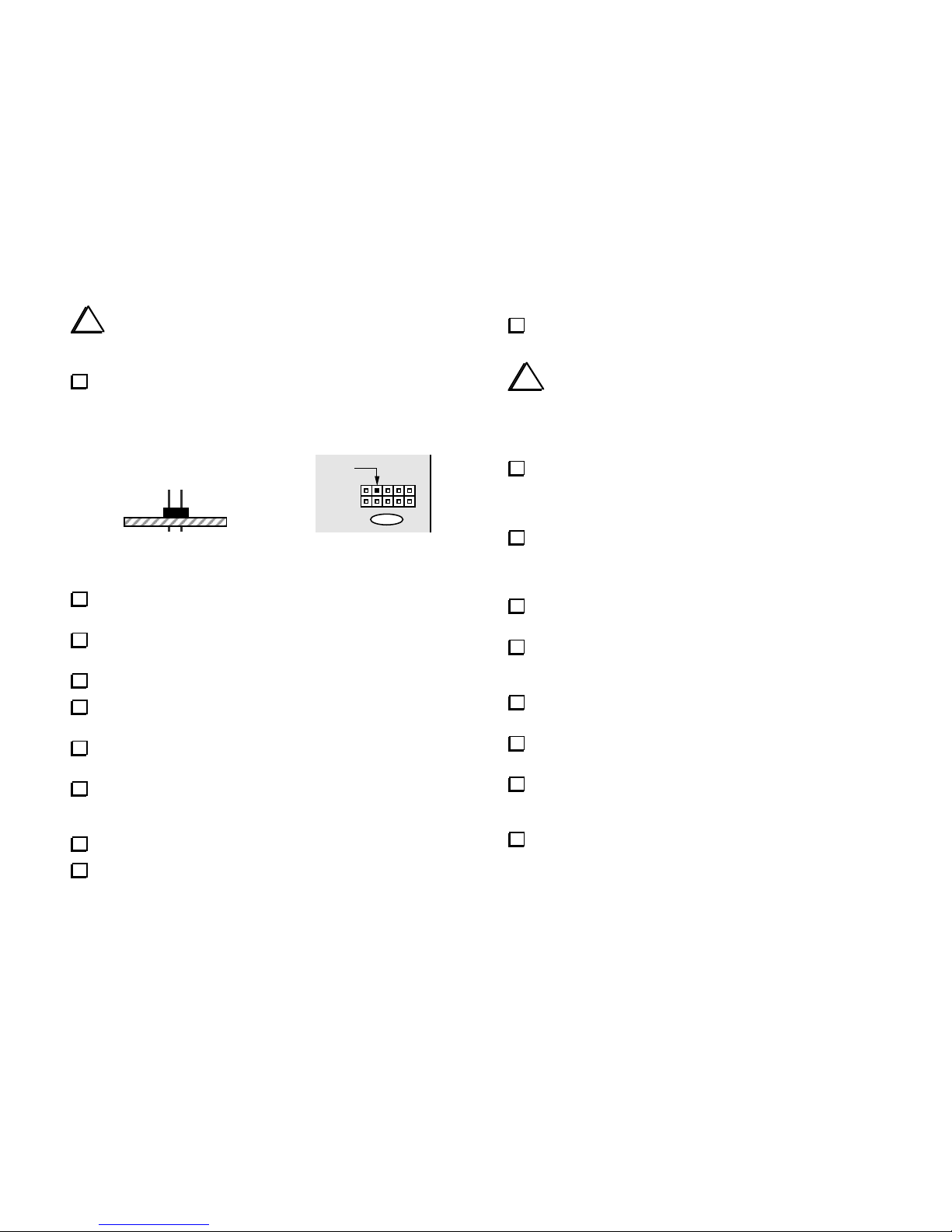
Install the 10-pin, dual-ro (5x2) male connector at P4, but do
not solder yet. Figure 3a sho s P4 as vie ed from right side of the
board. The plastic part of the connector must be on the top side of the
board, ith the long end of the pins pointed up. The short ends are
inserted into the board.
(a)
P4
(b)
P4
Pin 4
1
C46
Fig re 3
Solder just one pin of P4. Note: P4's plastic body can melt if too
much heat is applied. Limit soldering time to 2 to 3 seconds.
Examine P4 closely. If it is not flat against the board, re-heat the
soldered pin hile pressing do n on the plastic body of the connector.
Solder the remaining pins of P4. Do not trim the leads.
Cut pin 4 of P4 as indicated in Figure 3b, as close as possible to the
connector's plastic body.
Locate a 2-pin, high-current male connector (0.156" lead spacing)
for use at P3.
Install P3 at its indicated location on the right side of the board,
but do not solder yet. Make sure the polarizing tab is oriented as
indicated by its component outline.
Press P3 do n until it is flat against the board, then solder.
Install P6 (in the back-right corner) in the same manner as P3.
Install the 40-pin IC socket at U1. Orient the socket so the end
ith the open notch is to ard the right edge of the board.
i
In the following steps yo 'll be installing connectors at
the back edge of the PC board. These connectors m st be
installed correctly in order for the rear panel to fit onto the
board. Figure 13 (page 20) sho s ho the rear-panel connectors ill
appear once installed.
Install the DC input jack, J1, at the back edge. The 3 leads on the
jack must be lined up ith the slot-shaped holes in the component
outline. If the holes are a tight fit, press firmly until the connector
snaps into position, flat against the board. Solder all three pins.
Install the AUX RF jack, J2 (BNC), in the back-right corner.
Solder one of the large ground mounting pins first. If J2 then appears
to be tilted or t isted, reheat this ground pin hile pushing J2 do n
onto the board. Once it is seated properly, solder the remaining pins.
Install J3, the 9-pin "D" connector, as indicated by its component
outline. Do not solder yet.
Solder one of the 9 pins (near the center). Examine J3 closely. If
it is not flat against the board, re-heat the soldered pin hile pressing
do n on the connector. Then solder the remaining pins.
Solder J3's mounting tabs. Use a minimum of solder (do not fill
the entire hole).
Locate scre terminal E1. If it as supplied ith a scre , remove
it. The scre ill not be used.
Place E1 in its indicated position, ith the threaded hole facing
the rear edge of the board. Solder j st one pin. CAUTION: This
part ill get hot; don’t touch it ith your finger hile soldering.
If necessary, reheat the soldered pin of E1 and adjust it so that all
four pins are pressed do n on the board as far as they'll go. Then
solder all pins.

12
Locate voltage regulator U8 (78M05 or 7805). Bend the leads of
U8 to match its component outline (see Figure 4). Form the leads
around the shaft of a small scre driver to create smooth rather than
sharp bends.
U
se smooth bend
Fig re 4
Insert U8's leads into the proper holes. Secure U8 ith a 4-40 x
5/16" (8 mm) machine scre (zinc plated, not black), #4 lock asher,
and 4-40 nut.
Solder all three leads. Trim the leads on the bottom side.
Note: The pin 1 end of ICs can be identified by a notch or dimple as
sho n in Figure 5. This end must be oriented to ard the notched end
of the component outline.
Pin 1
Notch
Pin 1
Dimple
Fig re 5
Install U5 (LM358, 8 pins), hich is located in the back-right
corner. A portion of the part number is printed on the board under the
IC ("358"). Do not solder yet.
Bend t o opposite corner pins on the bottom side to hold the IC
in place. Solder all 8 pins (about 1 to 2 seconds per pin).
i
U2, 3, and 4 (TPIC6B595) are especially sensitive to
electrostatic discharge. To ch a gro nded s rface before
handling each of them.
Install the remaining ICs. Compare the part number on each IC to
the number printed on the board, and make sure that the pin 1 end is
oriented correctly.
__ U2, __ U3, and __ U4, TPIC6B595 (or similar number ending in "595")
__ U6, EL5146
Note: U7 is not used.
Remove the relays from their tube. If any of the pins are bent,
straighten them carefully using long-nose pliers.

13
Place relays at locations K1-K18. The relays can only be installed
one ay. Do not solder the relays yet, and do not clip or bend
the relay leads.
Using a thin hardcover book to hold the relays in place, flip the
PC board and book over together.
Solder just t o diagonally opposite corner pins on each relay.
Turn the board back over. If any relay is not flat against the
board, re-heat its corner pins one a time hile pressing do n on the
relay.
Once all relays are properly seated, solder the remaining pins. Do
not trim relay leads, hich can cause mechanical stress, reducing the
life of the relay.
Inductor Winding and Installation
A number of toroidal inductors are used on the RF board.1 The first
four inductors to be ound use type T80-0 cores. 80 specifies the
outside diameter in hundredths of an inch, in this case 0.80 inches
(20.3 mm). The -0 suffix refers to the core type, in this case
phenolic. In addition, four T94-2 cores are used (0.94", 24 mm). The
-2 refers to an iron powder core type.
There are also t o ferrite toroidal cores used, one of type FT37-43
and one of type FT50-43. In this part number, FT identifies the core
as ferrite, and -43 identifies the type of ferrite. The number in the
middle again specifies the outside diameter. 37, the smaller size, is
0.37" (9.5mm). 50, the larger size, is 0.50" (12.7mm). Both ferrite
cores are dark gray in color and can only be differentiated based on
their size.
Three types of enamel ire are supplied ith the kit: #20 red, #26 red,
and #26 green. #20 ire is much larger in diameter than #26. Be sure
to use only the type called for in the instructions; do not substitute
other ire types. Cut ires to the specified lengths to avoid running
out of ire.
1 Pre- ound toroids are available from an Elecraft-approved source; see page 3.
Sort the large toroidal cores into t o groups: bro n (T80-0, .80"
[20 mm]) and red (T94-2, 0.94" [24 mm]).
i
#20 enamel wire is q ite stiff. After winding it tightly
onto the core, yo may find that there's a small gap between
the wire and the core's flat s rfaces. This will not affect
performance. If yo try to wind the this wire so that it "h gs"
the core all the away aro nd, yo may have to p ll the wire too
hard, res lting in hand fatig e.
A T80-0 core (bro n phenolic) ill be used for L1. Cut 9 inches
(23 cm) of #20 red enamel ire. To ind L1, "se " the long end of
the ire through the core. Each pass through the core counts as one
turn. Exactly 6 turns are needed, as sho n in Figure 6. The enamel
insulation ill be removed in a later step.
Fig re 6
Place L1 on top of its photo (Figure 6). Adjust the turns until the
spacing is similar to that sho n. If the spacing cannot be matched, it
may be because you have one turn too fe or too many.
Trim L1's leads to about 3/4" [19 mm] long as sho n.

14
i
In the next two steps, the leads of L1 will be stripped
and tinned. Toroid leads m st be prepared correctly to
maintain reliability at the high voltages and c rrents seen by
the t ner.
There are three commonly-used methods to remove the enamel
coating from the leads: (1) heat-stripping, (2) burning/sanding, or (3)
scraping ith a sharp tool. These methods are covered belo .
(1) To heat-strip the enamel ire:
• Place a small amount of solder (a "blob") on the end of your
soldering iron
• Insert the clipped end of the ire into the hot solder. If the iron is
hot enough, you should see the insulation bubble and begin to
vaporize after 4 to 6 seconds.
• Add more solder and feed more of the ire into it as the enamel
melts. Continue tinning the ire up to the edge of the core. Then
slo ly pull the ire out of the solder.
• If any enamel remains on the lead, scrape it a ay using your
thumbnail or a sharp tool.
(2) The insulation can be burned off by heating it ith a butane lighter
for a fe seconds. Use sandpaper to remove the enamel residue.
(3) You can scrape the insulation off using a razor blade or other sharp
tool. Avoid nicking the ire.
Strip the leads of L1 as described above. Remove the enamel from
the leads up to the edge of the core (see Figure 6).
Tin L1's leads ith fresh solder. If the solder on the leads looks
dull or is not adhering very ell, remove any residual enamel and re-tin
the lead.
Install L1 flat on the board as sho n by its component outline
near relays K1 and K2. Do not solder yet.
Secure L1 to the PC board using a cable tie. T o holes are
provided for this purpose, one inside the core and one outside. The
cable tie should be installed such that its "head" (thick end) ends up on
the botto side, pressed tightly against the board (Figure 7).
Fig re 7
Using a ruler, make sure that the head of the cable tie does not
extend more than 0.25" (6 mm) belo the bottom of the board. This
ould prevent proper installation of the bottom cover.
Trim off excess cable tie length.
Solder the leads of L1. When soldering, make sure that the solder
binds ell to the leads. If the lead appears to be an "island" in a
pool of solder, it is not making good contact; remove the toroid
and prepare the leads as described above. (For further
information, look for "Soldering Tips" on our eb site.)
i
Do not apply adhesives or fixatives of any kind to toroids.
Using your DMM on a lo resistance scale, check for continuity
bet een L1's pads (not the leads) on the bottom of the board. If the
reading is over 1 ohm, re-strip the leads. Note: Your DMM probes ill
have some residual resistance. Short them together to measure this
amount, and subtract it from your continuity readings.

15
Toroidal inductors L2-L8 are sho n in the photos at right (Figure
8). Wind each of these toroids using the indicated cores, either T80-0
(bro n, phenolic) or T94-2 (red, iron po der). All are ound using
#20 enamel ire. Use the ire length and number of turns sho n.
Place each toroid on its photo and adjust the turns spacing so it is
similar to that sho n. Re-check turns counts. (Recall that each pass
through the core counts as one turn.)
Prepare the leads of these toroids as you did for L1.
i
The T94-2 cores (red) have one side hich is painted a darker
color than the rest of the core. To improve the appearance of the
completed RF board, e suggest mounting all four of these cores ith
the dark side do n.
Install L2-L8, using cable ties as you did for L1. Match each
toroid to its reference designator carefully. Exchanging any of them
ill make tune up erratic and may prevent the ATU from finding a
match.
Note: Once in position, some of the toroids may be very close to each
other, and may even be touching. This ill not affect performance.
Solder L2-L8.
On the bottom side of the board, check for continuity bet een
the pads of L2-L8. If you get a reading of over 1 ohm, remove the
toroid from the board and prepare the leads again.
__ L2: 10 T, T80-0 __ L3: 16 T, T80-0 __ L4: 23 T, T80-0
13" (33 cm) 19" (48 cm) 26" (66 cm)
__ L5, 12 T, T94-2 __ L6, 17 T, T94-2
18" (46 cm) 24" (61 cm)
__ L7, 24 T, T94-2 __ L8, 34 T, T94-2
34" (86 cm) 46" (117 cm)
Fig re 8

16
Locate the t o dark gray (ferrite) toroid cores. The smaller of
the t o (type FT37-43) has an outside diameter of 0.37" (9.5 mm).
This core ill be used in the follo ing steps.
RFC2 is ound on an FT37-43 core using 16 turns of #26 red
enamel ire (14", 36 cm). Wind and prepare this inductor in the same
manner as L1.
Install RFC2 vertically as indicated by its component outline near
relay K1.
i
Toroidal transformer T1 uses a bi-filar inding, hich means
that t o ires are ound on the core together. The ires ill be
t isted together loosely before they're ound onto the core.
Cut t o 11" (28 cm) lengths of #26 enamel ire, one red and
one green.
T ist the red and green ires together over their entire length.
The ires should cross over each other about every 1/2" (1 cm).
Wind 12 turns of the t isted ires onto the large ferrite core
(FT50-43). The turns should cover about 80-90% of the core, as
sho n in Figure 9 (a hite core as used to highlight the inding).
Separate T1’s leads as sho n in Figure 10. The numbers on the
leads correspond to numbered pads on T1's PC board outline.
Fig re 9
Strip and tin the leads of T1.
Using a magnifying glass, examine the red/green lead pairs to
make sure that the leads are not shorting together.
3
(RED)
2
(
GRN
)
1
(
GRN
)
4
(RED)
Fig re 10
Install T1 vertically on the PC board as indicated by its outline
near the back edge of the board. Insert the red and green leads into
their numbered holes (see lead numbering above).
Verify continuity bet een the #1 and #4 pads of T1.
17
Uninstalled Co ponents
Verify that these locations on the RF board are not filled:
Top side:
__ U1 (microcontroller, 16F877), should not be installed in its socket yet.
__ U7, front edge
__ W1-W6, front edge
__ W7, back edge
__ J7, right front corner
__ P7, right side, near L2
Top side, KAT100-1 only:
__ P6, __ P3, __ P4 (all along the right edge)
Bottom side:
__ R15 __ P1 __ P2 __ P5
P5 ill be installed in the next section. The other uninstalled
components are reserved for future use.
Visual Inspection
i
Nearly all problems with kits are ca sed by poorly-
soldered component leads or incorrectly-installed components.
Yo can locate and correct most assembly errors ahead of time
with a simple vis al inspection.
Using a magnifying glass, examine the bottom of the PC board
closely for all of the follo ing: cold solder joints (dull rather than
shiny appearance), solder bridges, and leads that are not soldered. Re-
heat any suspect joints.
Using the parts placement dra ing at the end of the appendix,
re-check the orientation of all __ Diodes, __ Transistors, __ ICs.
Resistance Checks
Make the resistance measurements listed belo , touching the
DMM's (+) and (-) leads to the indicated points. The schematic may be
helpful in troubleshooting any incorrect readings.
i
The symbol > means greater than. Your DMM may indicate
infinite resistance (all digits flashing) for readings in the table that
include this symbol. Other readings should be +/- 10 %.
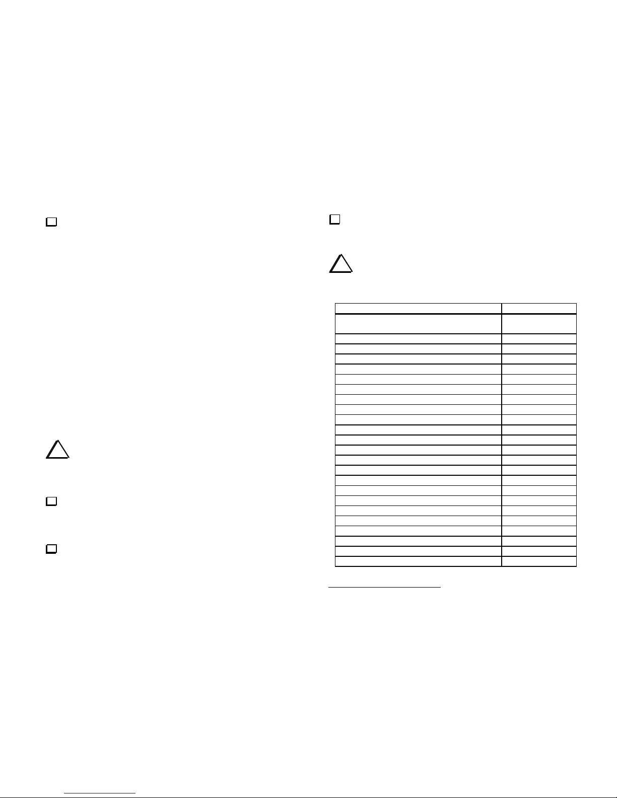
KAT100 Test Points (+, -) Resistance
Bet een pins 2 and 5 of relays K1-K18
(on bottom of board, marked)
380-450 ohms
U8 (voltage regulator) "12V" pin, ground 1-30 k
U8 (voltage regulator) "5V" pin, ground 1-30 k
U2 (6B595) pin 2, ground 1-30 k
U2 (6B595) pin 3, ground > 100 k
U2 (6B595) pin 9, ground < 2 ohms
U2 (6B595) pin 12, ground > 100 k
U2 (6B595) pin 13, ground > 100 k
U2 (6B595) pin 18, ground > 1 k
U6 (EL5146) pin 2, ground 1-30 k
U6 (EL5146) pin 3, ground > 1 k
U6 (EL5146) pin 6, ground > 1 k
U6 (EL5146) pin 7, ground 1-30 k
U6 (EL5146) pin 8, ground > 100 k
U5 (LM358) pin 1, ground > 100 k
U5 (LM358) pin 2, ground > 100 k
U5 (LM358) pin 3, ground 45-55 k
U5 (LM358) pin 5, ground 45-55 k
U5 (LM358) pin 6, ground > 100 k
U5 (LM358) pin 7, ground > 100 k
D3 (1N5817) cathode2, ground > 100 k
D3 (1N5817) anode, ground > 100 k
D4 (1N5817) cathode, ground > 100 k
D4 (1N5817) anode, ground > 100 k
2 The banded end is the cathode.

18
Front Panel Board Assembly
Place the Front Panel PC board in front of you ith the
"KAT100 FP" label at the left.
Install the follo ing t o resistors at the right edge:
__ R115, 220, 5% (red-red-brn)
__ R116, 470, 5% (yel-vio-brn)
Install 120-ohm resistors in all remaining resistor locations (R101
through R114).
Install the follo ing components on the bottom side of the board:
__ Q101 and __ Q102, PN2222A (align flat side as indicated)
__ C101 and __ C102, .047 (473)
i
TPIC6B595 ICs are very sensitive to static discharge.
To ch a gro nded, npainted metal s rface before handling
them.
Place a TPIC6B595 IC at U101, but do not solder yet. Note the
pin 1 location. The labeling on U101 should read upside-do n ith
respect to the "KAT100 FP" label.
While holding U101 firmly against the PC board, bend the four
corner pins on the IC out ard to hold it in place. The front panel
metal piece will not fit correctly nless U101 is seated flat on
the board.
Re-check the orientation of U101, then solder.
Install U102 in a similar fashion.
i
Follow all LED installation instr ctions caref lly to
preserve the appearance of yo r KAT100's front panel.
Sort the rectangular LEDs into groups according to color.
Install a green LED at D101, at the left end of the Front Panel
board, but do not solder yet. As indicated on the board, the long
lead (anode) goes to the right.
Hold the LED flat against the board (not tilted). Bend the leads
out ard on the bottom side to hold it in place. Then trim both leads.
Solder one lead of the LED, keeping soldering time to 1 to 2 sec.
If the LED is tilted or is not pressed flat against the board, re-heat
the lead hile pressing the LED do n.
Once the LED is correctly positioned, solder the other lead, again
keeping soldering time to 1-2 seconds.
Install a yellow LED at D102. Make s re the long lead is to
the right. Before soldering, adjust the LED's position as ith D101.
Install green LEDs at D103, D104, D105, and D106. Make sure
the long lead is to the right for these and all remaining LEDs.
Install yellow LEDs at D107, D108, and D109.
Install red LEDs at D110, D111, and D112.
Install a green LED at D113.
Install a yellow LED at D114.
Using a discarded component lead, make a 3/4" (19 mm) U-
shaped ire for the ground jumper ( ), near R101. Mount the jumper
ith the top of the U-shape no more than 1/8" (3 mm) above the
board. Solder from the bottom side.
Trim all leads as short as possible on both sides of the board.

19
Final Assembly
Straighten the leads of microcontroller IC U1 (PIC16F877) as
sho n belo . The ro s of pins must be straight and parallel to each
other to establish the proper pin spacing. To straighten the pins, rest
one ro of pins against a hard, flat surface. Press do n gently on the
other ro of pins and rock the IC for ard to bend the pins into
position as sho n belo .
Straight
Flared
Fig re 11
Insert U1 into its socket, ith the notched or dimpled end of the
IC aligned ith the notched end of its socket and outline. (The labeling
on the IC should be upside do n ith respect to the "KAT100 RF"
label at the left side of the board.)
Examine U1 closely. If any pins are bent, remove the IC and
straighten them. (To remove U1 from its socket, pry it up gently on
each end using a small flat-blade scre driver.)
i
The right side view at Fig re 12 shows how the Front
Panel and RF boards will be joined in the following steps.
J101 is a 12-pin female connector on the Front Panel board. P5 is a
12-pin right-angle male connector on the RF board. Also sho n is one
of t o L-brackets that secure the assembly and keep the Front Panel
board in a vertical position.
Locate the t o small L-brackets. Identify the shorter side of the
"L", hich ill be attached to the RF board.
Place an L-bracket at one of the indicated locations at the front
edge the RF board. Align it ith the component outline. If it's not
flush ith the front edge, the short and long sides may be reversed.
Secure the L-bracket loosely to the RF board using a 4-40 x 3/16"
[4.7 mm] scre (black) and #4 lock asher.
Install the second L-bracket in the same ay.
P5
Top of RF board
J
101
Fig re 12
Slide the 12-pin female connector (J101) onto the pins of the 12-
pin male connector (P5). There should be no gap bet een them.
Locate P5's outline on the botto of the RF board. Insert P5's
right-angle pins into their holes. Do not solder yet.
Position the Front Panel board as sho n above. The pins of J101
should be inserted into their holes, and the t o L-brackets should be
aligned ith their outlines on the back of the Front Panel board.
Secure the L-brackets loosely to the Front Panel using t o 4-40 x
3/16" [4.7 mm] scre s (black) and t o #4 lock ashers.
If the Front Panel is not aligned ith the RF board along its front
edge, adjust the L-brackets positions.
Tighten the all four L-bracket scre s.
Solder all pins of J101 and P5.

20
J6 J5 J4 E1 J3
J J1
Fig re 13
Un rap the rear panel piece, and place it ith the labeling facing
a ay from you. Revie Figure 13, hich sho s the vertical portion of
the panel, along ith all of the panel- and PCB-mounted connectors.
Do not attach the rear panel to the RF board at this time.
Using the supplied sandpaper or a sharp tool, scrape a ay any
residual paint from around the hole for the ground terminal, E1. Do
this on the inside s rface of the rear panel.
Sand or scrape residual paint from around at least one mounting
hole for each of the three SO239 connectors (J4, J5, and J6). Again,
this should be done on the inside surface.
Position J6 on the rear panel as sho n. The connector's flange
should be on the outside of the panel. The center pin's solder cup
should be facing up to facilitate soldering in a later step.
Secure J6 ith four 4-40 x 5/16" (8 mm) pan head scre s, #4 split
lock ashers, and 4-40 nuts. A solder lug takes the place of one lock
asher at the indicated corner, closest to the top edge of the rear
panel. Do not overtighten the hardware.
Position J5 and J4 on the rear panel in the same ay as J6, ith
the solder cups facing up.
Attach J5 and J4 to the rear panel using the same hard are. Note
the position of the solder lug on J5, hich differs from J4 and J6.
Cut six lengths of #20 stranded hookup ire (vinyl insulated):
__ three black, 1.25" (3.2 cm) long
__ t o red, 1.5" (4 cm) long
__ one red, 2.5" (6.3 cm) long.
Remove 1/4" (6 mm) of insulation from each end of all six ires.
T ist the strands of each ire tightly. Tin the ires using a small
amount of solder.
Table of contents
Other ELECRAFT Tuner manuals

ELECRAFT
ELECRAFT KAT500 User manual

ELECRAFT
ELECRAFT KXAT1 User manual

ELECRAFT
ELECRAFT KAT2 User manual

ELECRAFT
ELECRAFT KAT500 User manual

ELECRAFT
ELECRAFT KAT500 Installation manual

ELECRAFT
ELECRAFT T1 User manual

ELECRAFT
ELECRAFT KAT1 User manual

ELECRAFT
ELECRAFT KAT500 User manual

ELECRAFT
ELECRAFT KXAT2 User manual


