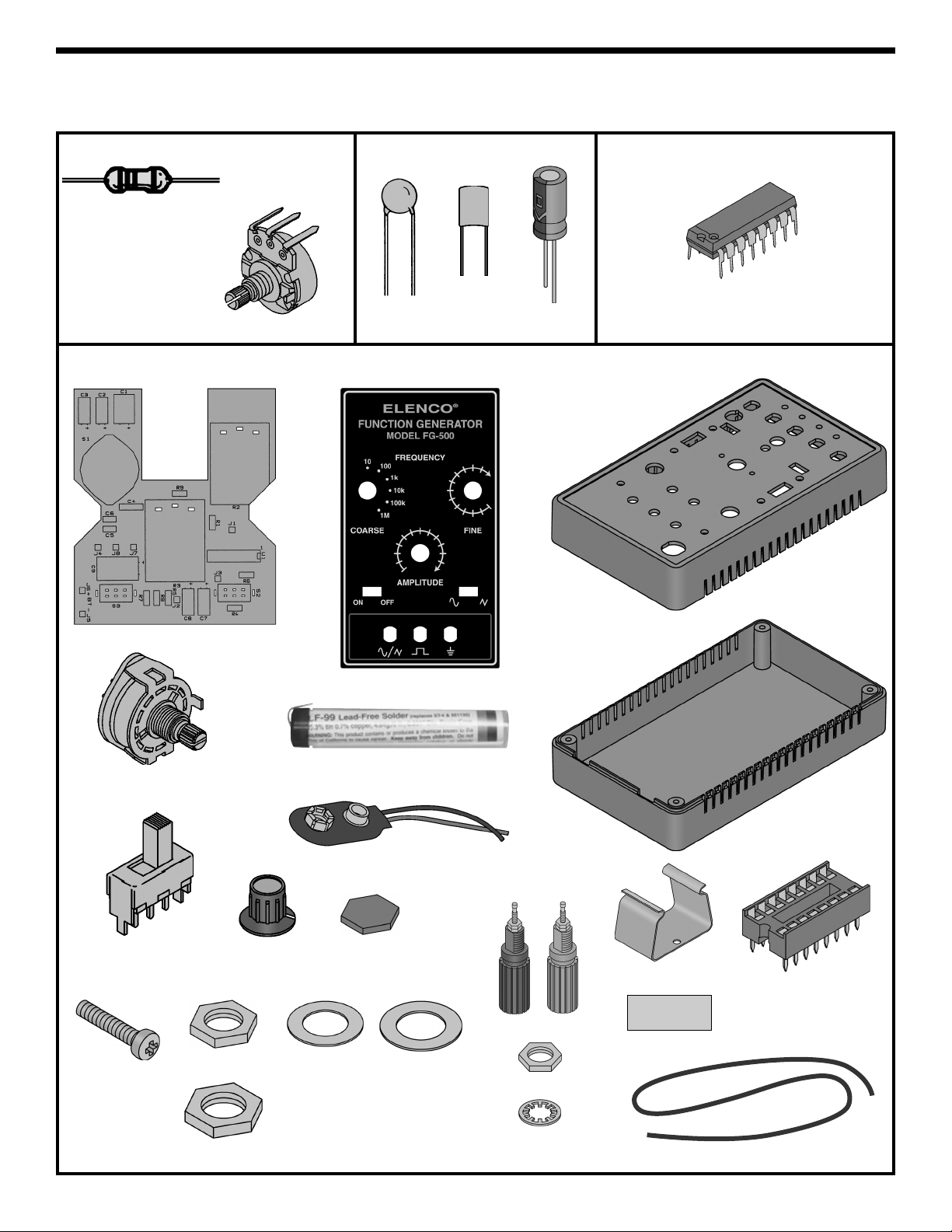
CONSTRUCTION
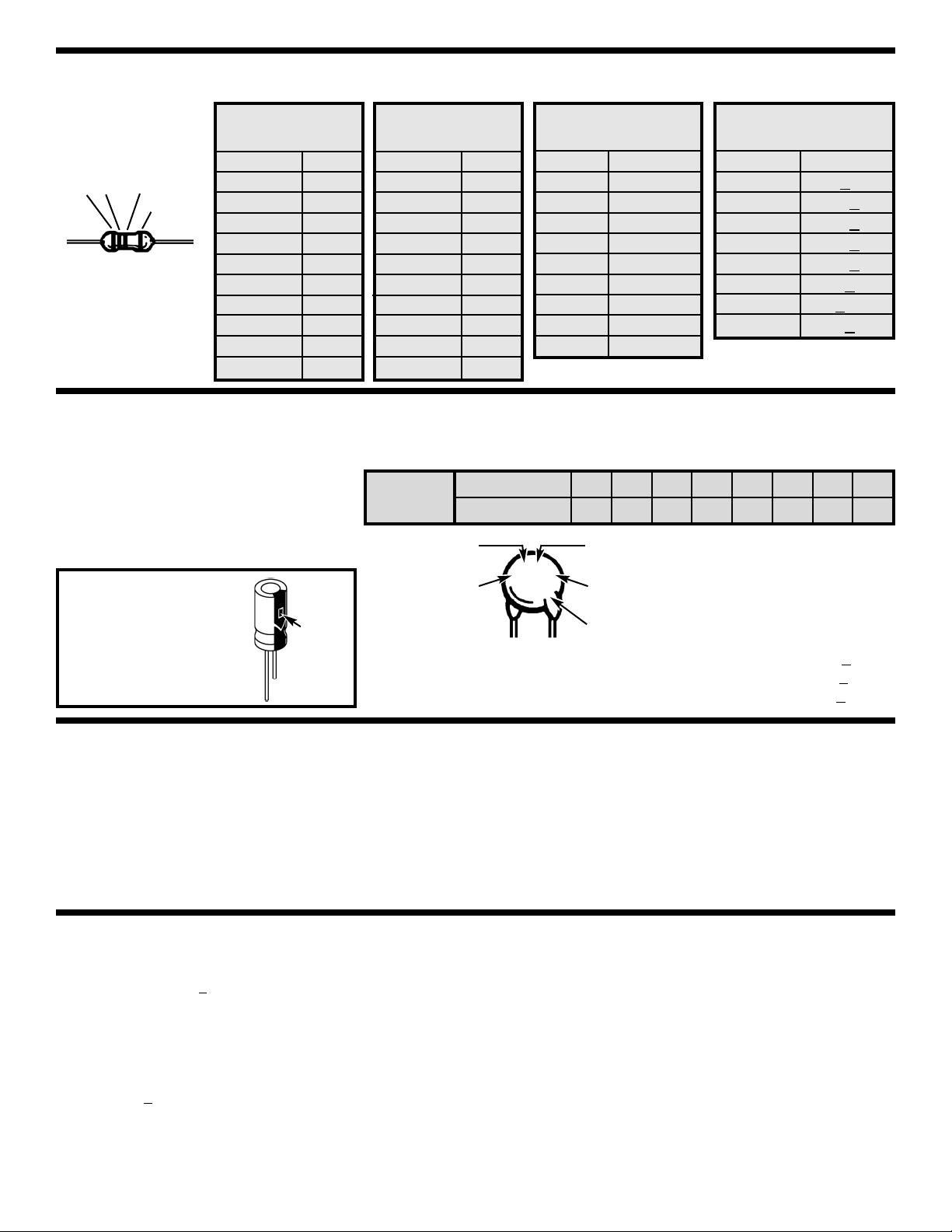
Solder Soldering Iron
Foil
Solder
Soldering Iron
Foil
Component Lead
Soldering Iron
Circuit Board
Foil
Rosin
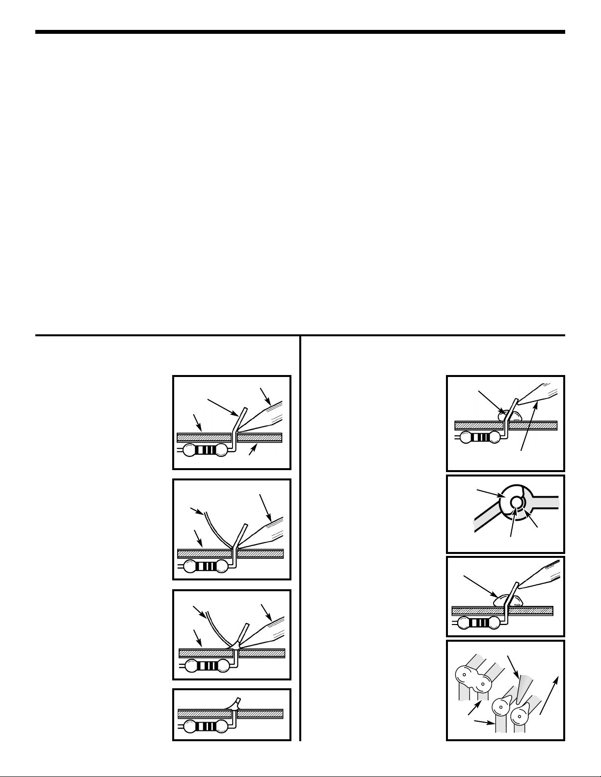
Soldering iron positioned
incorrectly.
Solder
Gap
Component Lead
Solder
Soldering Iron
Drag
Foil
1. Solder all components from the
copper foil side only. Push the
soldering iron tip against both the
lead and the circuit board foil.
2. Apply a small amount of solder to
the iron tip. This allows the heat to
leave the iron and onto the foil.
Immediately apply solder to the
opposite side of the connection,
away from the iron. Allow the
heated component and the circuit
foil to melt the solder.
1. Insufficient heat - the solder will
not flow onto the lead as shown.
3. Allow the solder to flow around
the connection. Then, remove
the solder and the iron and let the
connection cool. The solder
should have flowed smoothly and
not lump around the wire lead.
4.
Here is what a good solder
connection looks like.
2. Insufficient solder - let the
solder flow over the connection
until it is covered.
Use just enough solder to cover
the connection.
3. Excessive solder - could make
connections that you did not
intend to between adjacent foil
areas or terminals.
4. Solder bridges - occur when
solder runs between circuit paths
and creates a short circuit. This is
usually caused by using too much
solder.
To correct this, simply drag your
soldering iron across the solder
bridge as shown.
What Good Soldering Looks Like
A good solder connection should be bright, shiny, smooth, and uniformly
flowed over all surfaces.
Types of Poor Soldering Connections
Introduction
The most important factor in assembling your FG-500K Function
Generator Kit is good soldering techniques. Using the proper soldering
iron is of prime importance. A small pencil type soldering iron of 25 - 40
watts is recommended. The tip of the iron must be kept clean at all
times and well tinned.
Solder
For many years leaded solder was the most common type of solder
used by the electronics industry, but it is now being replaced by lead-
free solder for health reasons. This kit contains lead-free solder, which
contains 99.3% tin, 0.7% copper, and has a rosin-flux core.
Lead-free solder is different from lead solder: It has a higher melting
point than lead solder, so you need higher temperature for the solder to
flow properly. Recommended tip temperature is approximately 700OF;
higher temperatures improve solder flow but accelerate tip decay. An
increase in soldering time may be required to achieve good results.
Soldering iron tips wear out faster since lead-free solders are more
corrosive and the higher soldering temperatures accelerate corrosion,
so proper tip care is important. The solder joint finish will look slightly
duller with lead-free solders.
Use these procedures to increase the life of your soldering iron tip when
using lead-free solder:
• Keep the iron tinned at all times.
• Use the correct tip size for best heat transfer. The conical tip is the
most commonly used.
• Turn off iron when not in use or reduce temperature setting when
using a soldering station.
•
Tips should be cleaned frequently to remove oxidation before it becomes
impossible to remove. Use Dry Tip Cleaner (Elenco
®
#SH-1025) or Tip
Cleaner (Elenco
®
#TTC1). If you use a sponge to clean your tip, then use
distilled water (tap water has impurities that accelerate corrosion).
Safety Procedures
•Always wear safety glasses or safety goggles to
protect your eyes when working with tools or
soldering iron, and during all phases of testing.
• Be sure there is adequate ventilation when soldering.
•
Locate soldering iron in an area where you do not have to go around
it or reach over it. Keep it in a safe area away from the reach of
children.
•Do not hold solder in your mouth. Solder is a toxic substance.
Wash hands thoroughly after handling solder.
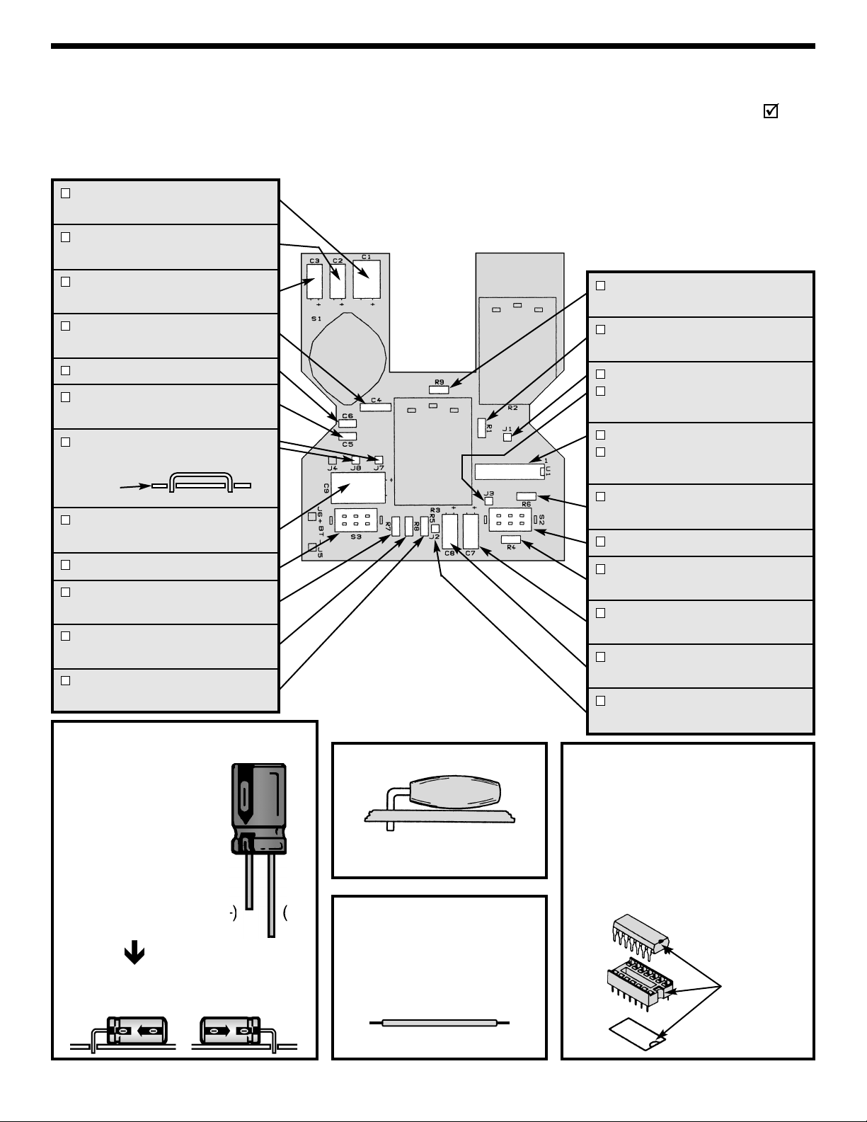
Assemble Components
In all of the following assembly steps, the components must be installed
on the top side of the PC board unless otherwise indicated. The top
legend shows where each component goes.The leads pass through the
corresponding holes in the board and are soldered on the foil side.
Use only rosin core solder.
DO NOT USE ACID CORE SOLDER!
'
-4-