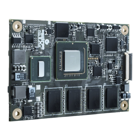
EMTRION emSTAMP-Argon User manual

Hardware Manual: emSTAMP- emSBC-Argon (Rev1)
1/35
emSTAMP-Argon
emSBC-Argon
Hardware Manual
including the emSTAMP-Argon processor module
and the emSBC-Argon development board
Rev1 / 30.09.2019
emtrion GmbH

Hardware Manual: emSTAMP- emSBC-Argon (Rev1)
2/35
© Copyright 2019 emtrion GmbH
All rights reserved. This documentation may not be photocopied or recorded on any electronic
media without written approval. The information contained in this documentation is subject to
change without prior notice. We assume no liability for erroneous information or its consequences.
Trademarks used from other companies refer exclusively to the products of those companies.
Revision: 1 / 30.09.2019
Rev
Date/Signature
Changes
0
25.07.2019/We
Preliminary revision
1
30.09.2019/We
First revision including the emSBC-Argon

Hardware Manual: emSTAMP- emSBC-Argon (Rev1)
3/35
Table of Content
1Introduction................................................................................................................................................................5
2Overview of the emSBC-Argon with embedded emSTAMP-Argon.......................................................5
3Handling Precautions..............................................................................................................................................6
4Functional Overview of the CPU module (emSTAMP-Argon)..................................................................6
5Functional description of the CPU module (emSTAMP-Argon) ..............................................................7
5.1 Processor.............................................................................................................................................................7
5.1.1 Processor Clocks.....................................................................................................................................8
5.1.2 Boot Configuration................................................................................................................................9
5.2 DDR3L SDRAM ..................................................................................................................................................9
5.3 QSPI-NOR Flash.................................................................................................................................................9
5.4 eMMC –NAND Flash interface................................................................................................................. 10
5.5 Ethernet............................................................................................................................................................ 10
5.6 USB 2.0.............................................................................................................................................................. 11
5.6.1 USB 2.0 Host.......................................................................................................................................... 11
5.6.2 USB 2.0 OTG........................................................................................................................................... 11
5.7 Display controller.......................................................................................................................................... 12
5.7.1 Display Serial Interface (DSI)............................................................................................................ 12
5.7.2 LCD-TFT display controller (LTDC) ................................................................................................ 13
5.8 FD-CAN ............................................................................................................................................................. 14
5.9 SD card interface........................................................................................................................................... 14
5.10 UART/USARTs................................................................................................................................................. 14
5.11 I2C Interface..................................................................................................................................................... 15
5.12 SPI Interface .................................................................................................................................................... 15
5.13 Serial Audio Interface (SAI)........................................................................................................................ 15
5.14 ADC and DAC ................................................................................................................................................. 16
5.14.1 Analog to Digital Converter (ADC)................................................................................................ 16
5.14.2 Digital to Analog Converter (DAC)................................................................................................ 16
5.15 GPIOs................................................................................................................................................................. 16
5.16 JTAG Debug.................................................................................................................................................... 17
5.17 Status LEDs...................................................................................................................................................... 17
5.18 User Power-On Key (PONKEY#)................................................................................................................ 17
5.19 Reset .................................................................................................................................................................. 18
5.20 Castellation Connector ............................................................................................................................... 19
5.21 Power Supply ................................................................................................................................................. 23
5.21.1 VIN Supply ............................................................................................................................................... 23
5.21.2 VBAT Supply.......................................................................................................................................... 23
5.21.3 +3V3 Supply.......................................................................................................................................... 23
5.21.4 VDD_SD .................................................................................................................................................. 23
5.21.5 USBH_VBUS........................................................................................................................................... 23
5.21.6 USB_OTG_VBUS................................................................................................................................... 23
6Functional Description of the Single-Board-Computer (emSBC-Argon)........................................... 24
6.1 eMMC NAND-Flash....................................................................................................................................... 24

Hardware Manual: emSTAMP- emSBC-Argon (Rev1)
4/35
6.2 microSD-Card socket................................................................................................................................... 25
6.2.1 Pinout of microSD-Card connector J6 ......................................................................................... 25
6.3 Ethernet Connector...................................................................................................................................... 26
6.3.1 Pinout ethernet connector J9......................................................................................................... 26
6.4 DSI-LCD............................................................................................................................................................. 26
6.4.1 Usage of LCD-Board MB1407.......................................................................................................... 26
6.4.2 Usage of LCD-Board B-LCD40-DSI1 .............................................................................................. 26
6.4.3 Pinout of DSI-Connector J3 ............................................................................................................. 27
6.5 USB 2.0 HOST.................................................................................................................................................. 28
6.5.1 Connector USB 2.0 Host J12............................................................................................................ 28
6.6 USB 2.0 OTG .................................................................................................................................................... 28
6.6.1 Pinout USB-OTG Connector J1 ....................................................................................................... 28
6.7 RPi Connector................................................................................................................................................. 29
6.8 FD-CAN Connector....................................................................................................................................... 30
6.9 UART connector ............................................................................................................................................ 30
6.10 Reset & Wake-up Buttons........................................................................................................................... 30
6.10.1 Reset Button S2.................................................................................................................................... 30
6.10.2 Wake-up Button S1............................................................................................................................. 31
6.11 Boot configuration DIP-Switch ................................................................................................................ 31
6.12 Battery holder................................................................................................................................................. 31
6.13 Board ID............................................................................................................................................................ 32
6.14 Power Supply ................................................................................................................................................. 32
7Technical Characteristics .................................................................................................................................... 33
7.1 Electrical Specifications .............................................................................................................................. 33
7.2 Environmental Specifications................................................................................................................... 33
7.3 Mechanical Specifications ......................................................................................................................... 33
7.4 Dimensional Drawing.................................................................................................................................. 34
7.4.1 emSTAMP-Argon (CPU module).................................................................................................... 34
7.4.2 emSBC-Argon (Single Board Computer)..................................................................................... 35

Hardware Manual: emSTAMP- emSBC-Argon (Rev1)
5/35
1Introduction
The emSTAMP-Argon processor module is a CPU board of emtrions emSTAMP-family, based on the
STM32MP157 processor from STMicroelectronics. The STM32MP157 has an ARM Cortex-A7 dual-
core and an ARM Cortex-M4.
The dual-core Cortex-A7 may be clocked up to 650MHz and includes a variety of functions required
for IOT, industrial or multimedia applications.
The CPU board is designed as a compact module with castellated mounting holes with 1.0mm
pitch that can be soldered directly on a baseboard. As an extension the CPU board has additional
solder pads on its bottom side which can be used if RGB- or JTAG-Interface are needed.
The emSBC-Argon development board is a SBC which is build around the CPU module. It provides
direct access to a set of the modules interfaces. It is targeted to quickly start into product
development.
The functionalities of the emSTAMP-Argon CPU board as well as the emSBC-Argon development
board are both documented in this manual.
2Overview of the emSBC-Argon with embedded emSTAMP-Argon

Hardware Manual: emSTAMP- emSBC-Argon (Rev1)
6/35
3Handling Precautions
Please read the following notes prior to installing the processor module. They apply to all ESD
(electrostatic discharge) sensitive components:
The module does not need any configurations before installing
The CPU module does not provide any on-board ESD protection circuitry –this must be
provided by the product it is used in.
Be sure all tools required for installation are electrostatic discharged as well.
Handle the board with care and try to avoid touching its components or tracks.
4Functional Overview of the CPU module (emSTAMP-Argon)
Block Diagram of the available Interfaces of the CPU module

Hardware Manual: emSTAMP- emSBC-Argon (Rev1)
7/35
5Functional description of the CPU module (emSTAMP-Argon)
5.1 Processor
The emSTAMP-Argon CPU module uses the STM32MP157CAC processor from STMicroelectronics.
The processor includes the ARM Cortex-A7 dual-cores (runs up to 650 MHz) and an ARM Cortex-M4
(runs up to 200 MHz). In addition to the CPU core, this processor provides a lot of features such as:
Secure Boot, TrustZone, DES/TDES/AES cryptographic acceleration, Secure ROM and RAM
NAND Flash controller (eMMC, SLC NAND-Flash)
DDR3(L) SDRAM controller
3D GPU (OpenGL ES 2.0) with 133Mpix/sec @533MHz
Ethernet MAC with 10/100 Mbit/s or 1Gbit/s
2 x USB 2.0 Host with high-speed mode
USB 2.0 OTG with high-speed mode
3x SDMMC/SDIO controller
LCD-TFT up to 24bpp and 1366x768 (WXGA) @60Hz
24 bit RGB interface TFT displays
MIPI DSI with 2 data lanes each up to 1GHz
8- to 14-bit parallel camera interface
2x FDCAN controller
serial interfaces:
o6 x I²C
o6 x SPI
o8 x U(S)ART
o4 x SAI (stereo audio)
Up to 29 Timer for encoder input, PWM output
2 x ADC (up to 16-bit resolution, up to 5Msps)
2 x DAC with 12-bit resolution and 1 MHz
JTAG debug interface
Real time clock

Hardware Manual: emSTAMP- emSBC-Argon (Rev1)
8/35
5.1.1 Processor Clocks
The processors high-speed external clock signal (HSE) is generated by an external 24MHz oscillator,
which is connected to the HSE_OSC_IN pin. Several internal dividers and PLLs multiply the 24 MHz
HSE input clock to the internal clocks. The SysClock is set to its maximum speed of 650 MHz.
A 32.768 KHz crystal is connected to the Low Speed External oscillator (LSE) of the processor. Its
main application is to generate the clock for the processors RTC. The emSTAMP-Argon module has
a dedicated pin for battery supply of the RTC block if the main power supply of the STM32MP157 is
turned off.
The STM32MP157 has two pins for “Microcontroller Clock Output”(MCO1 and MCO2) which are
connected to the castellated mounting holes. Each MCO has its own MUX and prescaler to select
the clock source of the MCO1 and MCO2 (see picture below).
Pinout of MCO1 and MCO2 on the emSTAMP-Argon module:
Module Pin
CPU Pin Name
Signal
Direction
(module view )
Termination
72
PG2
RCC_MCO_2
O
73
PI11
RCC_MCO_1
O
More information about the STM32P157 clock system is described in the chapter 10 “Reset and
Clock Control (RCC)” of the Reference manual from STMicroelectronics.

Hardware Manual: emSTAMP- emSBC-Argon (Rev1)
9/35
5.1.2 Boot Configuration
The STM32MP157 offers different boot modes which are selected by the three CPU pins BOOT[2:0].
The different boot modes which are available on the emSTAMP-Argon are shown in the table
below:
BOOT2
BOOT1
BOOT0
Initial boot mode
0
0
0
UART and USB
0
0
1
QUADSPI NOR-Flash
0
1
0
eMMC on SDMMC2 (only fitted on SBC)
1
0
1
SD-Card on SDMMC1
1
1
0
UART and USB
On the emSTAMP-Argon module the three boot configuration pins BOOT[2:0] are connected to 1k
pull-up resistor. The boot pins BOOT[2..0] are connected to the castellated mounting holes of the
module. The desired boot mode has to be set by appropriate setting of these three boot pins on
the carrier board.
Module Pin
CPU Pin Name
Signal
Direction
(module view )
Termination
3
BOOT0
BOOT0
I
PU 1K
4
BOOT1
BOOT1
I
PU 1K
5
BOOT2
BOOT2
I
PU 1K
Note: The emSBC-Argon provides a DIP-switch to set the different boot modes. Please refer to
chapter 6.11 “Boot configuration DIP-Switch” for details how to set the boot mode on the emSBC-
Argon by the DIP-switch.
5.2 DDR3L SDRAM
The emSTAMP-Argon CPU module provides up to 512MiB DDR3L SDRAM as main memory. The
RAM is connected via a 16 bit width data bus und may be clocked up to 533MHz.
5.3 QSPI-NOR Flash
A 16-Mibit QSPI-NOR flash memory (IS25LP016D form ISSI) is integrated on the CPU module. It is
used to hold the initial Bootloader that provides the basic boot functionality of the module. The
flash is connected to the QUAD-SPI bank1 with Quad-SPI-lines.
Module Pin
CPU Pin Name
Signal
-
PF8
QUADSPI_BK1_IO0
-
PF9
QUADSPI_BK1_IO1
-
PF7
QUADSPI_BK1_IO2
-
PF6
QUADSPI_BK1_IO3
-
PB6
QUADSPI_BK1_CS#
-
PF10
QUADSPI_CLK
Internal connection of QSPI-NOR-flash on the CPU-module

Hardware Manual: emSTAMP- emSBC-Argon (Rev1)
10/35
5.4 eMMC –NAND Flash interface
To store the operation system and application data, the CPU-module provides an eMMC-interface
to connect a NAND-Flash to the emSTAMP-Argon. It is connected to the 8-bit SDMMC2 interface of
the STM32MP157 and can be used a boot device.
Module Pin
CPU Pin Name
Signal
Direction
(module view )
Termination
98
PE3
SDMMC2_CK
O
SR 22R
99
PG6
SDMMC2_CMD
O
101
PB14
SDMMC2_D0
I/O
102
PB15
SDMMC2_D1
I/O
103
PB3
SDMMC2_D2
I/O
104
PB4
SDMMC2_D3
I/O
105
PA8
SDMMC2_D4
I/O
106
PA9
SDMMC2_D5
I/O
107
PE5
SDMMC2_D6
I/O
108
PC7
SDMMC2_D7
I/O
89
PF14
EMMC_RST#
O
The NAND Flash size can be between 4GB and 32GB depending on the ordering code.
Please contact emtrion GmbH for your required NAND Flash size.
5.5 Ethernet
The emSTAMP-Argon module provides an Ethernet interface with up to 100BASE-TX full duplex.
The Ethernet MAC interface of the STM32MP157 CPU is connected in RMII mode to the external
PHY LAN8720A from Microchip. The PHY address is set to 0.
A 25MHz clock is generated by the STM32MP157 on its ETH Clock Output (available at PB5) and
connected to the XTAL1/CLKIN of the PHY.
The reset input nRST of the PHY is controlled via the PA1 of the STM32MP157. An external 10k pull-
down resistor is connected to this signal to hold the PHY in reset during start-up of the CPU.
Module Pin
CPU Pin Name
Signal
-
PC1
ETH1_MDC
-
PA2
ETH1_MDIO
-
PA7
ETH1_CRS_DV
-
PC4
ETH1_RXD0
-
PC5
ETH1_RXD1
-
PB11
ETH1_TX_EN
-
PG13
ETH1_TXD0
-
PG14
ETH1_TXD1
-
PB5
ETH1_CLK
-
PA1
ETH1_RESET#
Internal connection of Ethernet-MAC interface on the CPU-module

Hardware Manual: emSTAMP- emSBC-Argon (Rev1)
11/35
The PHY LAN8720A is integrated on the CPU module so that an Ethernet Jack (with integrated
magnetics) may be directly connected to the modules Ethernet pins ETH_RDP/ETH_RDM and
ETH_TDP/ETH_TDM which are available at the castellated mounting holes of the module. An
appropriate 1:1 transformer with a 100nF capacitor to GND and a 3.3V supply at each center tap pin
must be added externally. Link or traffic indication signals for additional LEDs are not provided.
Module Pin
CPU Pin Name
Signal
Direction
(module view )
Termination
19
-
ETH_TDM
AO
20
-
ETH_TDP
AO
22
-
ETH_RDM
AI
23
-
ETH_RDP
AI
5.6 USB 2.0
The STM32MP157 contains two high-speed PHYs. The processor provides an USB 2.0 high-speed
host controller and an USB 2.0 OTG high-speed controller.
5.6.1 USB 2.0 Host
The STM32MP157 provides an USB 2.0 compliant host interface, supporting data transfers at low-
speed (1.2 Mbit/s), full-speed (12 Mbit/s) and high-speed (480Mbps).
The VBUS supply voltage is provided by the PMIC of the emSTAMP-Argon. Over-current protection
is done by the PMIC.
Module Pin
CPU Pin Name
Signal
Direction
(module view )
Termination
50
USB_DP1
USBH_HS1_DP
AI/O
51
USB_DM1
USBH_HS1_DM
AI/O
52
-
USBH VBUS
Power output
5.6.2 USB 2.0 OTG
The STM32MP157 provides an USB 2.0 compliant OTG interface, supporting data transfers at full-
speed (12 Mbit/s) and high-speed (480Mbps).
Module Pin
CPU Pin Name
Signal
Direction
(module view )
Termination
40
PA10
USB_OTG_HS_ID
I
41
-
USB_OTG VBUS
Power I/O
43
USB_DP2
USB_OTG_HS_DP
AI/O
44
USB_DM2
USB_OTG_HS_DM
AI/O
If the USB_OTG_HS_ID signal (PA10) is tied to GND (logical “0”) by an external device/connector,
the CPU module enters host mode. A floating ID signal places the CPU in device mode.

Hardware Manual: emSTAMP- emSBC-Argon (Rev1)
12/35
5.7 Display controller
The STM32MP157 provides two display controllers with different interfaces:
a MIPI-DSI host controller with two data lanes
a LCD-TFT display controller provides a 24-bit parallel digital RGB
The parallel 24-bit RGB-interface of LCD-TFT display controller has a special feature on the
emSTAMP-Argon module. All pins 24-bit RGB interface are connected to SMD-pads on the bottom
side of the module (see picture below).
The DSI-interface is connected to the castellated mounting holes on the edge of the module.
5.7.1 Display Serial Interface (DSI)
The MIPI-DSI-Interface of the STM32MP157 supports two data lanes with 1Gbit/s. The DSI controller
supports color mapping of a16, 18 and 24-bit RGB. The pixel clock for the display data can be
generated by an internal PLL. More information about the DSI interface of the STM32P157 system
can be found in chapter 36 “DSI Host” of the Reference manual of STMicroelectronics.
Module Pin
CPU Pin Name
Signal
Direction
(module view )
Termination
90
DSI_D1P
DSI_D1_P
O
91
DSI_D1N
DSI_D1_N
O
92
-
GND
Power
93
DSI_CKN
DSI_CLK_N
O
94
DSI_CKP
DSI_CLK_P
O
95
-
GND
Power
96
DSI_D0P
DSI_D0_P
O
97
DSI_D0N
DSI_D0_N
O

Hardware Manual: emSTAMP- emSBC-Argon (Rev1)
13/35
5.7.2 LCD-TFT display controller (LTDC)
The LCD-TFT display controller (LTDC) of the STM32MP157 provides a parallel RGB interface with
up to 24-bit color (RGB-888). This interface supports a wide range of LCD- and TFT-panels with up
to WXGA (1366 x 768) @ 60 fps. As control signals it provides V-Sync, H-Sync, pixel clock and data
enable. The LTDC has two display layers each with 64 x 64-bit FIFO.
The following table shows the LTDC color output in RGB-888, RGB-666 and RGB-565 format. If less
than 8-bit per color are used (RGB-666 and RGB-565), the RGB data lines of the LCD panel must be
connected to the MSB of the LTDCs RGB data lines.
LTDC on
module
LCD RGB-888
LCD RGB-666
LCD RGB-565
LTDC_B0
LCD-B0
LTDC_B1
LCD-B1
LTDC_B2
LCD-B2
LCD-B0
LTDC_B3
LCD-B3
LCD-B1
LCD-B0
LTDC_B4
LCD-B4
LCD-B2
LCD-B1
LTDC_B5
LCD-B5
LCD-B3
LCD-B2
LTDC_B6
LCD-B6
LCD-B4
LCD-B3
LTDC_B7
LCD-B7
LCD-B5
LCD-B4
LTDC_G0
LCD-G0
LTDC_G1
LCD-G1
LTDC_G2
LCD-G2
LCD-G0
LCD-G0
LTDC_G3
LCD-G3
LCD-G1
LCD-G1
LTDC_G4
LCD-G4
LCD-G2
LCD-G2
LTDC_G5
LCD-G5
LCD-G3
LCD-G3
LTDC_G6
LCD-G6
LCD-G4
LCD-G4
LTDC_G7
LCD-G7
LCD-G5
LCD-G5
LTDC_R0
LCD-R0
LTDC_R1
LCD-R1
LTDC_R2
LCD-R2
LCD-R0
LTDC_R3
LCD-R3
LCD-R1
LCD-R0
LTDC_R4
LCD-R4
LCD-R2
LCD-R1
LTDC_R5
LCD-R5
LCD-R3
LCD-R2
LTDC_R6
LCD-R6
LCD-R4
LCD-R3
LTDC_R7
LCD-R7
LCD-R5
LCD-R4
The following table shows the available signals of the parallel 24-bit RGB interface. The pinout of
the pins can be found in the chapter “Castellation Connector”.
Signal
Description
LTDC_R[7..0]
8-bit red color data
LTDC_G[7..0]
8-bit green color data
LTDC_B[7..0]
8-bit blue color data
LTDC_HSYNC
horizontal sync signal
LTDC_VSYNC
vertical sync signal
LTDC_CLK
Pixel clock
LTDC_DE
Data enable

Hardware Manual: emSTAMP- emSBC-Argon (Rev1)
14/35
5.8 FD-CAN
The emSTAMP-Argon supports both CAN modules of the STM32MP157 (FDCAN1 and FDCAN2).
Both are compliant with ISO 11898-1 (CAN protocol specification version 2.0 part A, B) and CAN FD
protocol specification version 1.0.
Module Pin
CPU Pin Name
Signal
Direction
(module view )
Termination
13
PB13
FDCAN2_TX
O
14
PB12
FDCAN2_RX
I
34
PD1
FDCAN1_TX
O
35
PD0
FDCAN1_RX
I
5.9 SD card interface
For the SD card interface the SDIO port (SDMMC1) of the STM32MP157 is used. The interface is 4-
bit wide and compatible with the SD Memory Card Specification Version 3.01 SDR50.
Module Pin
CPU Pin Name
Signal
Direction
(module view )
Termination
56
PB7
SDMMC1_CD#
I
57
PC11
SDMMC1_D3
I/O
58
PC10
SDMMC1_D2
I/O
59
PC9
SDMMC1_D1
I/O
60
PC8
SDMMC1_D0
I/O
61
PD2
SDMMC1_CMD
O
62
PC12
SDMMC1_CK
O
The interface SDMMC1 can be used as boot device during SD card boot. Minimum set of required
signals for SD card boot are in bold.
5.10 UART/USARTs
The emSTAMP-Argon provides 3 U(S)ART interfaces on its castellated mounting holes. The USART
ports USART2 and USART3 are both implemented with CTS/RTS flow control. The UART4 port is
used as UART interface without flow control. All ports are able to communicate at speeds up to
10Mbit/s.
Module Pin
CPU Pin Name
Signal
Direction
(module view )
Termination
36
PG11
UART4_TX
O
37
PB2
UART4_RX
I
64
PB10
USART3_TX
O
65
PD9
USART3_RX
I
66
PG8
USART3_RTS
O
67
PD11
USART3_CTS
I
79
PD3
USART2_CTS
I
80
PD4
USART2_RTS
O
81
PD6
USART2_RX
I
82
PD5
USART2_TX
O

Hardware Manual: emSTAMP- emSBC-Argon (Rev1)
15/35
5.11 I2C Interface
Up to six I2C bus interface are available at the STM32MP157. The interfaces I2C1 and I2C5 are
directly connected as LVTTL signals to the castellated mounting holes of the module. At both I2C
interfaces there are no pull-up resistors equipped on the emSTAMP-Argon module. The pull-up
resistors have to be added on the carrier board.
The I2C interfaces and support standard (up to 100 Kbit/s) and fast mode (up to 400 Kbit/s) and fast
mode-plus (up to 1Mbit/s). They also support SMBus 2.0 and PMBus 1.1.
Module Pin
CPU Pin Name
Signal
Direction
(module view )
Termination
75
PA12
I2C5_SDA
I/O
76
PA11
I2C5_SCL
O
77
PF15
I2C1_SDA
I/O
78
PD12
I2C1_SCL
O
5.12 SPI Interface
On the emSTAMP-Argon module the SPI1 interface is directly connected to the castellated
mounting holes. SPI1 can communicate at up to 50Mbit/s.
Module Pin
CPU Pin Name
Signal
Direction
(module view )
Termination
68
PZ0
SPI1_SCK
O
69
PZ3
SPI1_CS#
O
70
PZ2
SPI1_MOSI
O
71
PZ1
SPI1_MISO
I
5.13 Serial Audio Interface (SAI)
The STM32MP157 offers a serial audio interface (SAI) with two independent sub-blocks. The SAI
supports audio protocols like I2S (LSB or MSB-justified), PCM/DSP, TDM, AC’97 and SPDIF (SPDIF
only as transmitter. The SAI supports sampling frequencies up to 192 KHz. The data size may be 8,
10, 16, 20, 24 or 32bits.
On the emSTAMP-Argon module the SAI2 of the STM32MP157 is connected to the castellated
mounting holes. A master clock output signal is also connected.
Module Pin
CPU Pin Name
Signal
Direction
(module view )
Termination
45
PF11
SAI2_SD_B
I
46
PI6
SAI2_SD_A
O
47
PI5
SAI2_SCK_A
O
48
PE0
SAI2_MCLK_A
O
49
PI7
SAI2_FS_A
O

Hardware Manual: emSTAMP- emSBC-Argon (Rev1)
16/35
5.14 ADC and DAC
The emSTAMP-Argon module provides 3 pins on its castellated mounting holes which are
dedicated for analog input and output functionality. The ADC and the DAC use the same reference
voltage which is supplied at the VREF+ pin of the CPU. On the emSTAMP-Argon the VREF+ pin is
connected to 3.3V
5.14.1 Analog to Digital Converter (ADC)
The STM32MP157 provides two independent analog to digital converter with up to 16 bit
resolution. The two ADCs can be configured to work in simultaneous or interleaved conversion
mode. ADC2 can also be used to monitor VBAT, internal DAC1, internal DAC2 and the internal
temperature sensor.
Module Pin
CPU Pin Name
Signal
alternative port function
15
PF12
GPIO_01
ADC1_INP6, ADC1_INN2
38
PA5
DAC1_OUT2
ADC1_INP19, ADC1_INN18,
ADC2_INP19, ADC2_INN1,
39
PA4
DAC1_OUT1
ADC1_INP18, ADC2_INP18
5.14.2 Digital to Analog Converter (DAC)
The DAC can be configured to run in 8- or 12-bit mode.
Module Pin
CPU Pin Name
Signal
38
PA5
DAC1_OUT2
39
PA4
DAC1_OUT1
5.15 GPIOs
The emSTAMP-Argon module offers 8 free to use GPIO[7..0], on its castellated mounting holes.
GPIO[7..3] additionally offer PWM as alternative port function.
There are 5 more GPIO[12-8] which are used for control functions on the emSBC-Argon (see table
below). On a new carrier board GPIO[12..8] can be used in a different way.
Module Pin
CPU Pin Name
Signal
Used on emSBC-
Argon as
Alternate port
function
16
PE7
GPIO_00
15
PF12
GPIO_01
ADC1_INP6, ADC1_INN2
88
PE1
GPIO_02
8
PH14
GPIO_03
TIM8_CH2N
9
PD13
GPIO_04
TIM4_CH2
10
PH11
GPIO_05
TIM5_CH2
11
PE9
GPIO_06
TIM1_CH1
12
PE8
GPIO_07
TIM1_CH1N
83
PZ6
GPIO_08
MAC_EEPROM_WP#
84
PC6
GPIO_09
DSI_TE
85
PZ7
GPIO_10
DSI_RESET#
86
PF2
GPIO_11
TOUCH_IRQ
87
PA15
GPIO_12
BACKLIGHT_CTRL
TIM2_CH1

Hardware Manual: emSTAMP- emSBC-Argon (Rev1)
17/35
5.16 JTAG Debug
For programming and debugging the STM32MP157 offers two interfaces:
Serial Wire Debug (SWD)
JTAG Debug
Both interfaces are available via the same pins on the SMD pads on the bottom side of the module.
Module Pin
CPU Pin Name
Signal
Direction
(module view )
Termination
137
JTCK-SWCLK
JTCK_SWCLK
I
IPD
138
JTMS-SWDIO
JTMS_SWDIO
I
IPU
139
JTDI
JTDI
I
IPU
140
JTDO-TRACESWO
JTDO
O
IPU
141
NJTRST
JTRST#
I
IPU
5.17 Status LEDs
A dual-color (red and green) status LED is placed on the CPU module. The LEDs are connected to
the port pins of CPU via series resistors. The LEDs have a positive logic, i.e. the LEDs are turned on if
the output set to high. The LEDs may be used as custom specific indicators.
Module Pin
CPU Pin Name
Signal
Direction
(module view )
Termination
-
PA13
LED_RED
n.a.
SR 100R
-
PA14
LED_GREEN
n.a.
SR 100R
5.18 User Power-On Key (PONKEY#)
The PONKEY# signal may be used to wake the PMIC (power management IC) from powersave
states (OFF, STOP and STANDBY). The PONKEY# has an internal pull-up resistor in the PMIC and
should be driven by open drain/collector outputs, or connected to GND through a switch. If
unused, leave this pin open.
Module Pin
CPU Pin Name
Signal
Direction
(module view )
Termination
7
-
PONKEY#
I
IPU

Hardware Manual: emSTAMP- emSBC-Argon (Rev1)
18/35
5.19 Reset
The STM32MP157 CPU has an internal power supply supervisor, which includes an integrated
power-on-reset (POR) and a power-down reset (PDR). On the emSTAMP-Argon CPU module the
POR and PDR circuitry is always enabled by setting the PDR_ON pin of the CPU to high. The
emSTAMP-Argon module provides 2 pins with reset functionality on its castellated mounting holes:
Module Pin
CPU Pin Name
Signal
Direction
(module view )
Termination
17
-
RESET_MICO#
I
PU 10K
18
PG0
RESET_MOCI#
O
The emSTAMP-Argon module provides a RESET_MICO# pin (Module_In_Carrierboard_Out) on
which an external reset signal may be applied to reset the CPU module. The RESET_MICO# Pin has
an external pull-up resistor and should be driven by open drain/collector outputs, or connected to
GND through a switch. If unused, leave this pin open.
The RESET-MOCI# pin (Module_Out_Carrierboard_In) of the module provides access to the
onboard reset network. It might be used to reset peripherals on the baseboard while the CPU is
also in reset state. The RESET-MOCI# signal uses LVTTL level and is active low. RESET_MOCI# can be
controlled via the GPIO output pin PG0 of the STM32MP157.
The RESET_MOCI# signal should never be driven by the user. Use the RESET_MICO# signal to
provide an external reset.

Hardware Manual: emSTAMP- emSBC-Argon (Rev1)
19/35
5.20 Castellation Connector
For the placement and the orientation of the 108 castellated mounting holes of the emSTAMP-
Argon module, please refer to chapter “Dimensional Drawing”.Abbreviations:
AI analogue input
AO analogue output
I digital input
O digital output
I/O digital bidirectional
PU xK x KΩ pullup resistor
PD xK x KΩ pulldown resistor
SR xR x Ω series resistor
IPU xK processor internal x KΩ pullup resistor
IPD xK transistor internal x KΩ pulldown resistor

Hardware Manual: emSTAMP- emSBC-Argon (Rev1)
20/35
In the following table the castellated mounting holes are referred to as “Module Pins”. The “CPU
pin name”refers to the STM32MP157 in the TFBGA-361 ball package.
Module Pin
CPU Pin Name
Signal
Direction
(module view )
Termination
1
-
+3V3
Power output
2
-
GND
Power
3
BOOT0
BOOT0
I
PU 1K
4
BOOT1
BOOT1
I
PU 1K
5
BOOT2
BOOT2
I
PU 1K
6
VBAT
VBAT
Power input
7
-
PONKEY#
I
IPU
8
PH14
GPIO_03 (TIM8_CH2N)
I/O
9
PD13
GPIO_04 (TIM4_CH2)
I/O
10
PH11
GPIO_05 (TIM5_CH2)
I/O
11
PE9
GPIO_06 (TIM1_CH1)
I/O
12
PE8
GPIO_07 (TIM1_CH1N)
I/O
13
PB13
FDCAN2_TX
O
14
PB12
FDCAN2_RX
I
15
PF12
GPIO_01
I/O
16
PE7
GPIO_00
I/O
17
-
RESET_MICO#
I
PU 10K
18
PG0
RESET_MOCI#
O
19
-
ETH_TDM
AO
20
-
ETH_TDP
AO
21
-
GND
Power
22
-
ETH_RDM
AI
23
-
ETH_RDP
AI
24
-
GND
Power
25
-
GND
Power
26
-
GND
Power
27
-
GND
Power
28
-
VIN
Power input
29
-
VIN
Power input
30
-
VIN
Power input
31
-
VIN
Power input
32
-
VIN
Power input
33
-
VIN
Power input
34
PD1
FDCAN1_TX
O
35
PD0
FDCAN1_RX
I
36
PG11
UART4_TX
O
37
PB2
UART4_RX
I
38
PA5
DAC1_OUT2
O
39
PA4
DAC1_OUT1
O
40
PA10
USB_OTG_HS_ID
I
41
-
USB_OTG VBUS
Power I/O
42
-
GND
Power
43
USB_DP2
USB_OTG_HS_DP
AI/O
44
USB_DM2
USB_OTG_HS_DM
AI/O
45
PF11
SAI2_SD_B
I
46
PI6
SAI2_SD_A
O
47
PI5
SAI2_SCK_A
O
48
PE0
SAI2_MCLK_A
O
49
PI7
SAI2_FS_A
O
50
USB_DP1
USBH_HS1_DP
AI/O
This manual suits for next models
1
Table of contents
Other EMTRION Computer Hardware manuals
