EMTRION emSTAMP Helium User manual

emSTAMP Helium (Rev3)
1/23
emSTAMP Helium
Hardware Manual
including the Helium SBC development board and the CPU module
Rev3 / 25.06.2020

emSTAMP Helium (Rev3)
2/23
© Copyright 2020 emtrion GmbH
All rights reserved. This documentation may not be photocopied or recorded on any
electronic media without written approval. The information contained in this documentation
is subject to change without prior notice. We assume no liability for erroneous information or
its consequences. Trademarks used from other companies refer exclusively to the products of
those companies.
Revision: 3 / 25.06.2020
Rev
Date/Signature
Changes
1
25.04.2018/Sk
First revision
2
26.03.2020/Bue
Update concerning HW Revision 2
3
25.06.2020/Sk
Adding FUSE-Configuration
Clarify Pin Numbering on EDT-Display Connector

emSTAMP Helium (Rev3)
3/23
Table of Content
1Introduction...................................................................................................................................................... 5
2Overview of the Helium development SBC board............................................................................. 6
3Handling Precautions.................................................................................................................................... 7
4Functional Overview...................................................................................................................................... 8
4.1 List of features......................................................................................................................................... 8
5Functional Description (Helium CPU module)...................................................................................10
5.1 Boot Configuration and Fuse-Bits..................................................................................................10
5.2 DDR3 SDRAM ........................................................................................................................................10
5.3 NOR –Flash............................................................................................................................................10
5.4 NAND-Flash............................................................................................................................................10
5.5 Display Interface...................................................................................................................................10
5.5.1 Color mapping in 16/18bit mode.........................................................................................11
5.5.2 EDT display connector pinout ................................................................................................12
5.6 Ethernet....................................................................................................................................................12
5.7 Analog to Digital Converter .............................................................................................................13
5.8 Status LEDs .............................................................................................................................................13
5.9 Recovery Pin...........................................................................................................................................13
5.10 Base Power Enable Signal .................................................................................................................13
5.11 WAKEUP Signal .....................................................................................................................................13
5.12 Reset..........................................................................................................................................................13
5.13 Power Supply.........................................................................................................................................14
5.13.1 Overview.........................................................................................................................................14
5.13.2 +3V3 Supply..................................................................................................................................14
5.13.3 Backup Supply..............................................................................................................................14
5.13.4 VDD_ANA.......................................................................................................................................14
5.13.5 VDD_SDMMC................................................................................................................................14
5.14 Castellation Connector.......................................................................................................................15
6Functional Description of Helium SBC board ....................................................................................17
6.1 Micro SD-Card.......................................................................................................................................17
6.2 Ethernet....................................................................................................................................................17
6.3 USB 2.0 HOST ........................................................................................................................................17
6.4 USB 2.0 Device/OTG............................................................................................................................18
6.5 WiFi/BT.....................................................................................................................................................18
6.6 TPM............................................................................................................................................................19
6.7 CAN ...........................................................................................................................................................19
6.8 Debug console ......................................................................................................................................19
6.9 Reset & Wakeup...................................................................................................................................20

emSTAMP Helium (Rev3)
4/23
6.10 Backup Battery.......................................................................................................................................20
6.11 Base LEDs ................................................................................................................................................20
6.12 Power Supply.........................................................................................................................................20
6.12.1 5 V Supply......................................................................................................................................21
6.12.2 3.3 V Supply ..................................................................................................................................21
7Technical Characteristics............................................................................................................................22
7.1 Electrical Specifications......................................................................................................................22
7.2 Environmental Specifications...........................................................................................................22
7.3 Mechanical Specifications.................................................................................................................22
7.3.1 Drawing of SBC developer board .........................................................................................23

emSTAMP Helium (Rev3)
5/23
1Introduction
emSTAMP-Helium processor module is a CPU board of emtrion’s emSTAMP-family, based on
the ATSAMA5D27/28 processor from Microchip. The processor core may be clocked up to
500MHz and includes a variety of functions required for IOT, industrial or multimedia
applications.
The processor board is designed as a compact module with castellated edge contacts that
can be soldered directly on a baseboard.
The emSTAMP-Helium development board is an SBC build around the CPU module. It
provides direct access to a set of the module’s interfaces. It is targeted to quickly start into
product development.
The functionalities of the Helium development SBC board as well as those of the module are
both documented in this manual.
emSTAMP Helium (Rev3)
6/23
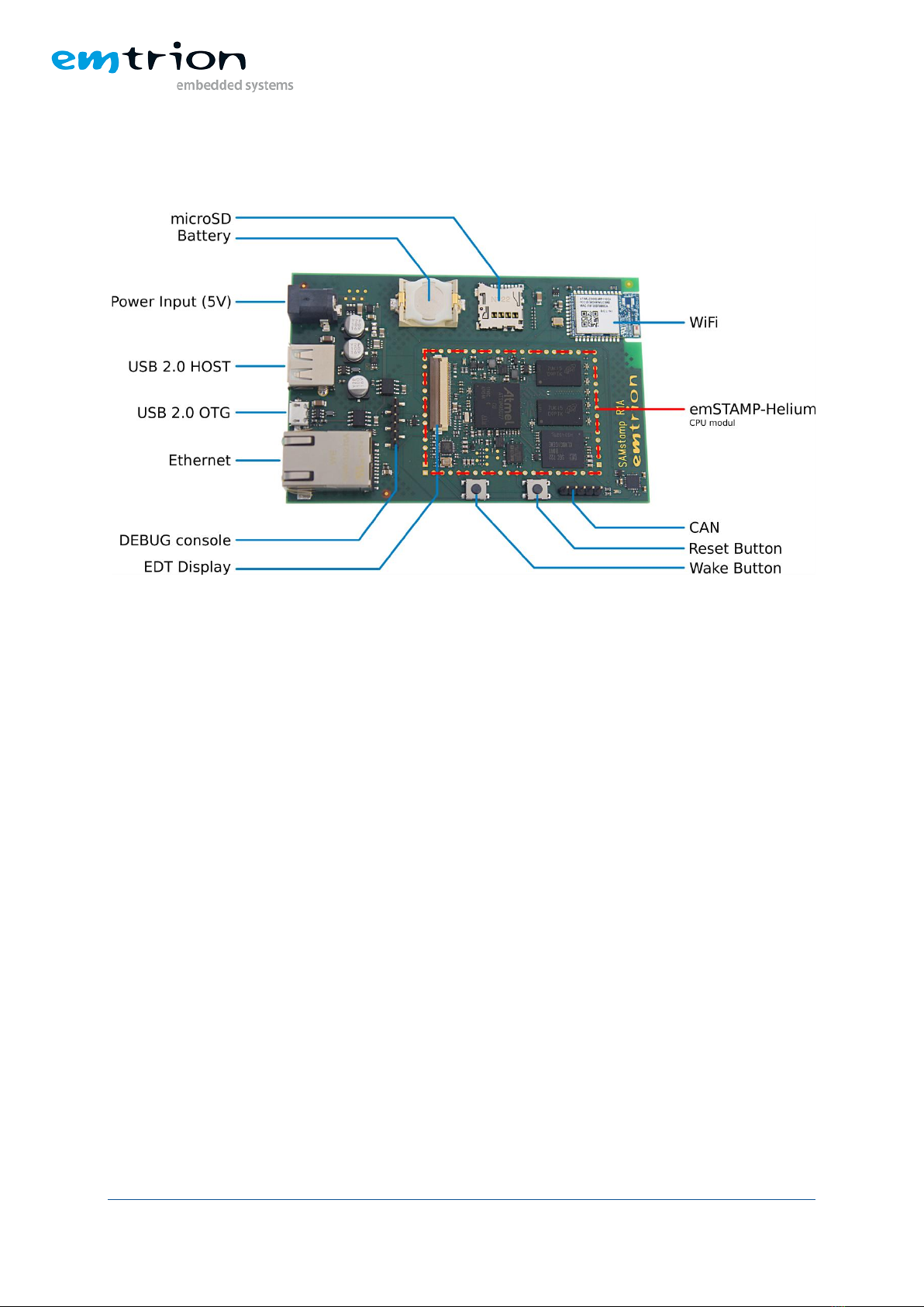
2Overview of the Helium development SBC board

emSTAMP Helium (Rev3)
7/23
3Handling Precautions
Please read the following notes prior to installing the processor module. They apply to all
ESD (electrostatic discharge) sensitive components:
•The module does not need any configurations before installing
•The CPU module does not provide any on-board ESD protection circuitry –this must
be provided by the product it is used in.
•Before installing the module, it is recommended that you discharge yourself by
touching a grounded object.
•Be sure all tools required for installation are electrostatic discharged as well.
•Before installing (or removing) the module, unplug the power cable from your mains
supply.
•Handle the board with care and try to avoid touching its components or tracks.

emSTAMP Helium (Rev3)
8/23
4Functional Overview
Block Diagram of the available Interfaces of the CPU module
4.1 List of features
The emSTAMP-Helium processor module uses the ATSAMA5D2 processor from Atmel. It
Includes the ARM Cortex-A5 core and runs up to 500 MHz.
In addition to the CPU core, this processor provides a lot of features such as:
•NAND Flash controller
•DDR3 SDRAM controller
•Ethernet MAC 10/100Mbit compatible with the IEEE802.3 standard
•USB 2.0 Host with high-speed mode
•USB 2.0 OTG with high-speed mode
•SDMM Card host controller
•LCD Controller for TFT displays up to 1024x768 (XGA) @60Hz and 16/18 bpp
•18-bit RGB interface for EDT TFT displays with integrated capacitive touch controller
(resistive touch on request)
•CAN controller
•UART with 32-byte FIFO

emSTAMP Helium (Rev3)
9/23
•Flexcom interfaces providing the following serial interfaces:
oI²C
oSPI
oU(S)ART
•Sound Interface with I²S format
•JTAG debug interface
•PWM
•Real time clock

emSTAMP Helium (Rev3)
10/23
5Functional Description (Helium CPU module)
5.1 Boot Configuration and Fuse-Bits
The fuse bits are set to boot U-Boot from the NOR-Flash integrated on the module. U-Boot
may be used to load software from additional media such as NAND-Flash or SD-Card. Refer
to the software manual for further details.
The DISABLE_BSCR bit is not set so that the user may overwrite the boot configuration using
BUREG but this is not recommended and not supported by emtrion. For further details of this
feature refer to section Standard Boot Strategies of the SAMA5D2 Series datasheet.
5.2 DDR3 SDRAM
The emSTAMP-Helium CPU module provides up to 512MB DDR3 SDRAM as main memory.
The RAM is connected via a 32-bit width data bus und may be clocked up to 125MHz.
Please contact emtrion GmbH for your required RAM size.
5.3 NOR –Flash
A 4 MB NOR-Flash memory is integrated on the CPU module. It is used to hold the initial
Bootloader that provides the basic boot functionality of the module.
The memory is connected to the SPI0 (CS0) interface of the processor.
5.4 NAND-Flash
An eMMC NAND Flash is provided on the emSTAMP-Helium module to store the operating
system and application data. The storage is connected to the SDMMC0 interface of the
processor. The NAND Flash size is depending on the ordering code.
Please contact emtrion GmbH for your required NAND Flash size.
5.5 Display Interface
The LCD controller of the ATSAMA5D27A-CU can drive TFT displays with resolutions up to
1024 x 768 (XGA) at 16/18 bpp. The pixel clock for the display data can be generated by an
internal PLL. A TFT LCD display may be connected to the EDT display connector. The pinout
of the connector conforms to a family of TFT displays that is available from the company EDT.
Besides that, other TFT displays may also be connected with an appropriate adapter.
emSTAMP Helium (Rev3)
11/23
In principal these displays are offered either with integrated 4-wire resistive touch interface or
with projected capacitive touch interface. The connector J1 supports both touch interfaces.
The capacitive touch controller is connected to the I²C interface on the FLEXCOM3 interface
of the CPU. The touch controller’s wake input is driven by PC18 signal. The touch controller’s
interrupt output is connected to the PC21 signal. Further details about the touch controller
can be found in the display’s data sheet.
The brightness of the backlight can be controlled by the PWM signal on pin PC18 (LCDPWM).
The following table describes the function of the data and control lines.
Signal
Description
LCD_D[xx]
18 color data; can also be used in 16-bit mode
LCD_VSYNC
Vertical synchronization signal
LCD_HSYNC
horizontal synchronization signal
LCD_DEN
Data enable signal, if active color data are valid
LCD_CLK
Display clock
LCD_DISP
Backlight power enable signal
LCD_PWM
PWM signal to control the backlight
5.5.1 Color mapping in 16/18bit mode
The following table shows the RGB colour mapping on the LCD_D[xx] pins of the emSTAMP
connector.
LCD_D[xx]
RGB565 (16bit)
RGB666 (18bit)
LCD_D2
-
B0
LCD_D3
B0
B1
LCD_D4
B1
B2
LCD_D5
B2
B3
LCD_D6
B3
B4
LCD_D7
B4
B5
LCD_D10
G0
G0
LCD_D11
G1
G1
LCD_D12
G2
G2
LCD_D13
G3
G3
LCD_D14
G4
G4
LCD_D15
G5
G5
LCD_D18
-
R0
LCD_D19
R0
R1
LCD_D20
R1
R2
LCD_D21
R2
R3
LCD_D22
R3
R4
LCD_D23
R4
R5
emSTAMP Helium (Rev3)
12/23
5.5.2 EDT display connector pinout
Type: Hirose FH12-40
EDT Pin
Helium Pin
Signal
1
40
RESET#
2
39
RESET#1
3
38
BLUE5
4
37
BLUE4
5
36
BLUE3
6
35
BLUE2
7
34
BLUE1
8
33
BLUE0
9
32
GND
10
31
GREEN5
11
30
GREEN4
12
29
GREEN3
13
28
GREEN2
14
27
GREEN1
15
26
GREEN0
16
25
GND
17
24
RED5
18
23
RED4
19
22
RED3
20
21
RED2
EDT Pin
Helium Pin
Signal
21
20
RED1
22
19
RED0
23
18
GND
24
17
LCD_PCLK_OUT
25
16
GPIO_WAKE#
26
15
LCD_HSYNC
27
14
LCD_VSYNC
28
13
LCD_DE
29
12
LCD_BL_EN
30
11
LCD_VCC
31
10
GND
32
9
GND
33
8
LCD_VCC
34
7
LCD_VCC
35
6
IRQ_TOUCH2#
36
5
LCD_BL_CTRL
37
4
SCL_LCD
38
3
n/c
39
2
SDA_LCD
40
1
n/c
5.6 Ethernet
The emSTAMP-Helium module provides an Ethernet interface with up to 100BASE-TX full
duplex. The PHY is integrated on the CPU module so that an Ethernet Jack (with integrated
magnetics) may be directly connected to the modules Ethernet pins.
The Ethernet signal lines are connected to the mounting holes of the Helium PCB edges. An
appropriate 1:1 transformer with a 100nF capacitor to GND and a 3.3V supply at each center
tap pin must be added externally.
Link or traffic indication signals for additional LEDs are not provided.
1
This pin can also be connected to GND by
assembly variation

emSTAMP Helium (Rev3)
13/23
5.7 Analog to Digital Converter
The emSTAMP-Helium module can perform analog to digital conversion on up to 12 Pins.
Tha ADC provides 12-bit Resolution, with Enhanced Mode up to 14 bits. The ADC may also
be used as resistive 4-wire and 5-wire Touchscreen Controller.
The reference voltage for the analog to digital converter should be applied to VDD_ANA pin.
5.8 Status LEDs
A dual-color status LED is placed on the CPU module. The LEDs are connected to the PWM
capable Pins PB6 and PB8 and may be used for custom specific indicators.
5.9 Recovery Pin
The recovery pin may be used to force the software into a recovery state. For details see the
software documentation.
Leave this pin unconnected if not used.
5.10 Base Power Enable Signal
The BASE_PWR_EN signal is used to disable the peripherals on the baseboard while the CPU
is in low power/sleep mode. This signal is low during sleep states and goes high when the
CPU starts up or returns to normal state.
5.11 WAKEUP Signal
The WAKEUP Signal may be used to wake the CPU from power save states. The WAKEUP Pin
has an internal pull-up resistor and should be driven by open drain/collector outputs, or
connected to GND through a switch. If unused, leave this pin open.
5.12 Reset
The module provides a RESETIN# Pin on which an external reset signal may be applied. The
RESETIN# Pin has an internal pull-up resistor and should be driven by open drain/collector
outputs, or connected to GND through a switch. If unused, leave this pin open.
The RESET# Pin of the module provides access to the onboard reset network. It might be
used to reset peripherals on the baseboard while the CPU is also in reset state. The RESET#
signal uses LVTTL level and is active low.

emSTAMP Helium (Rev3)
14/23
The RESET# signal should never be driven by the user. Use the RESETIN# signal to provide an
external reset.
5.13 Power Supply
5.13.1 Overview
Supply
Direction
Vmin
Vtyp
Vmax
+3V3
to module
3.10V
3.3V
3.50V
V_BACKUP
to module
1.65V
3.60V
VDD_ANA
to module
2.00V
3.3V
3.60V
VDD_SD_MMC
from module
3.3V
5.13.2 +3V3 Supply
The Module will be powered by a single +3V3 supply. No additional supplies are required to
use the basic functionality of the module.
5.13.3 Backup Supply
To use the standby/sleep capabilities of the module a 3V supply to the V_BACKUP pin is
required.
A 3V lithium coin cell may be used to provide this supply. V_BACKUP is internal ORed with
the +3V3 supply by diodes.
5.13.4 VDD_ANA
VDD_ANA is the reference voltage of the ADC. It is internally connected to +3V3.
VDD_ANA can be connected to the internal +3V3 supply on the module via a filter. Please
contact emtrion if you are interested in that feature.
5.13.5 VDD_SDMMC
VDD_SDMMC is the supply voltage for the SD-Card interface. It is internally connected to
+3V3.

emSTAMP Helium (Rev3)
15/23
5.14 Castellation Connector
3554
120
68
55
21
34
Pin
Signal
Alt
PIO A
PIO B
PIO C
PIO D
PIO E
PIO F
1
PD23
AD4
URXD2
FLEXCOM4_IO2
I2SC0_DO0
2
PD29
AD10
SPI1_NPCS1
FLEXCOM2_IO3
TIOA3
TWD0
3
PD24
AD5
UTXD2
FLEXCOM4_IO3
4
PD26
AD7
SPI1_MOSI
FLEXCOM2_IO0
5
WAKEUP
6
USB A D-
7
USB A D+
8
USB B D+
9
USB B D-
10
VDD_ANA
11
PD25
AD6
SPI1_SPCK
FLEXCOM4_IO4
12
PD30
AD11
SPI1_NPCS2
FLEXCOM2_IO4
TIOB3
TWCK0
13
PC0
FLEXCOM0_IO4
TWCK0
14
PD28
AD9
SPI1_NPCS0
FLEXCOM2_IO2
15
PD27
AD8
SPI1_MISO
FLEXCOM2_IO1
16
PC4
TIOB1
SPI1_NPCS0
I2SC0_DI0
17
PC5
TCLK1
SPI1_NPCS1
I2SC0_DO0
18
PC2
CANRX0
SPI1_MOSI
I2SC0_MCK
19
PC1
CANTX0
SPI1_SPCK
I2SC0_CK
20
PC3
TIOA1
SPI1_MISO
I2SC0_WS
21
PA31
PWML0
CLASSD_L3
22
GND
23
PA30
PWMH0
SDMMC1_CD
CLASSD_L2
24
PA22
SDMMC1_SCK
25
PA19
TIOA0
SDMMC1_DAT1
26
PA18
SDMMC1_DAT0
27
VDD_SDMMC
28
PA28
TIOB1
SDMMC1_CMD
CLASSD_L0
29
PA21
IRQ
TCLK0
SDMMC1_DAT3
30
PA20
TIOB0
SDMMC1_DAT2
31
PA29
TCLK1
SDMMC1_WP
CLASSD_L1
32
GND
33
GND
34
GND
35
GND
36
GND
37
PD5
TWCK1
UTXD2

emSTAMP Helium (Rev3)
16/23
38
PD4
TWD1
URXD2
39
RECOVERY
40
RESETIN#
41
RESET#
42
GND
43
V_BACKUP
44
+3V3
45
+3V3
46
PB2
CLASSD_R1
47
PB3
URXD4
IRQ
CLASSD_R2
48
PB4
UTXD4
FIQ
CLASSD_R3
49
GND
50
PD31
ADTRG
IRQ
TCLK3
51
PB31
FLEXCOM0_IO3
TWD0
52
PB30
FLEXCOM0_IO2
TCLK5
53
PB29
FLEXCOM0_IO1
TIOB5
54
PB28
FLEXCOM0_IO0
TIOA5
55
GND
56
BASE_PWR_EN
57
PB1
PWML1
CLASSD_R0
58
PD21
AD2
TIOB2
TWD0
FLEXCOM4_IO0
I2SC0_WS
59
PD20
AD1
TIOA2
UTXD2
I2SC0_MCK
60
PD22
AD3
TCLK2
TWCK0
FLEXCOM4_IO1
I2SC0_DI0
61
PD19
AD0
PCK0
URXD2
I2SC0_CK
62
DEBUG_TXD
63
DEBUG_RXD
64
ETH_TD-
65
ETH_TD+
66
ETH_RD-
67
ETH_RD+
68
GND

emSTAMP Helium (Rev3)
17/23
6Functional Description of Helium SBC board
As the SBC uses the module as its core all module specifications are also valid for the SBC.
The following section describes the interfaces connected to the outside pins of the module.
6.1 Micro SD-Card
A micro SD-Card socket is available. All signals are directly connected to the processor
module interface SDMMC1 without any further provisions. A write protect signal line is not
provided.
Pin
Signal
1
D2 (PA20)
2
D3 (PA21)
3
CMD (PA28)
4
VDD (VDD_SDMMC)
5
CLK (PA22)
6
GND
7
D0 (PA18)
8
D1 (PA19)
9
CD (PA30)
10
GND
6.2 Ethernet
A 10/100 MBit Ethernet interface is available via RJ45 connector. The center taps of the
magnetics are connected to a 3.3V DC supply. There no traffic or Link LEDs available.
Pin
Signal
1
n/c
2
n/c
3
TD+ (ETH_TDP)
4
TXC
5
TD- (ETH_TDM)
6
RD+ (ETH_RDP)
7
RXC
8
RD- (ETH_RDM)
9
n/c
10
GND
11
n/c
12
n/c
6.3 USB 2.0 HOST
A USB2.0 Host interface is provided to connect USB devices such as a keyboard, mouse,
printer or memory stick.

emSTAMP Helium (Rev3)
18/23
The USB host interface is realized by the internal host controller of the processor. It is
compliant to the USB specification Rev. 2.0, supporting data transfers at low-speed
(1,5Mbps), full-speed (12 Mbps) and high-speed (480Mbps).
The control line USBB_PEN (PC3) from the processor module is connected to a power switch
to control the bus supply. A logical “1” switches the power on, a logical “0” turns the power
off.
Pin
Signal
1
VBUS
2
D- (HHSDPB)
3
D+ (HHSDMB)
4
GND
6.4 USB 2.0 Device/OTG
The USB 2.0 micro A/B port can operate in Host or Device mode. The signal USBA_ID (PC5) is
used to determine the mode of the connected device.
The interface is realized by the internal device controller of the processor. The interface is
USB 2.0 compliant, supporting data transfers at low-speed (1,5Mbps), full-speed (12 Mbps)
and high-speed (480Mbps).
If the ID signal (PC5) is tied to GND (logical “0”) by an external device/connector, the CPU
module enters host mode. A floating ID signal places the CPU in device mode.
In host mode bus supply can be controlled via the power switch connected to the control line
USBA_PEN (PC4). A logical “0” switches the power on, a logical “1” turns the power off.
Pin
Signal
1
VBUS
2
D- (HHSDMA)
3
D+ (HHSDPA)
4
ID (PC5)
5
GND
6.5 WiFi/BT
An IEEE 802.11 b/g/n link controller module with integrated Bluetooth 4.0 is placed on the
SBC. The Module is connected to FLEXCOM0 (UART mode), FLEXCOM4 (SPI mode), UART2
and some GPIOs.
emSTAMP module
WiFI/BT module
PD23
SPI_SCK
PD22
SPI_MISO

emSTAMP Helium (Rev3)
19/23
PD21
SPI_MOSI
PD24
SPI_CS
PB29
BT_TXD
PB28
BT_RXD
PB31
BT_CTS
PC0
BT_RTS
PD20
WIFI/BT_TXD
PD19
WIFI/BT_RXD
PB30
WIFI/BT_EN
PB2
WIFI/BT_IRQ#
PA29
WIFI/BT_RST#
6.6 TPM
The SBC includes a TPM that may securely store cryptographic keys and perform
cryptographic actions.
The TPM is connected to the I²C interface TWI0 of the CPU module (PD29 and PD30). PD 28 is
used as reset signal for the TPM.
6.7 CAN
The processor on the Helium module includes a CAN controller, which is compliant to the CAN
protocol specification 2.0 Part A, B and ISO 11898-1 supporting both standard and extended
message frames. The LVTTL transmit and receive signals of the CAN channel are directly
connected from the Helium module to the pin header. Additionally, 3.3 V supply and GND are
provided. The signal level is 3,3V. The maximum baud rate is 1Mbps.
For a connection to a CAN network a transceiver must be connected to the pin header.
Emtrion’s ADA-CAN_3V3 may be used.
Pin
Signal
1
3.3V
2
GND
3
TX (PC1)
4
RX (PC2)
5
n/c
6.8 Debug console
The Helium module has a serial port which is used for debugging. The serial port is integrated
in the processor and available as LVTTL level. The connections are ESD and EMI protected. The
pinout is compatible to FTDIs TTL-232R-3V3 USB-to-serial cable.

emSTAMP Helium (Rev3)
20/23
Pin
Signal
1
GND
2
n/c
3
n/c
4
RX (DEBUG_RXD)
5
TX (DEBUG_TXD)
6
n/c
6.9 Reset & Wakeup
The WAKEUP (WKUP) Signal is directly connected to the processor. The signal uses a active-
low logic. An external button is added on the SBC developer board to use the WAKE function.
The RESETIN# signal is connected to a reset circuit on the Helium module and is asserted
with logic “0”. An external button is added on the SBC developer board to use the RESET
function.
6.10 Backup Battery
By the V_BAK Signal, the processor on the Helium module can be supplied by an external
battery. An external battery holder is added on the SBC developer board.
6.11 Base LEDs
With two PWM signals (PA31 and PB1), two status indication LEDs can be driven from the
processor on the Helium module. The LEDs are added on the SBC developer board.
6.12 Power Supply
The Helium SBC developer board has a power supply input at power socket. The base board
should be supplied with +5 V (± 5%) with a maximum power consumption of t.b.d. W. The
voltage is protected from reverse polarity.
Table of contents
Popular Control Unit manuals by other brands


Huawei
Huawei MU509 Series Acceptance Inspection Guide

Samson
Samson 2406 Mounting and operating instructions

JED
JED JED T440 manual

Honeywell
Honeywell NOTIFIER FCM-1 Installation and maintenance instructions

Graco
Graco EnDure instruction manual

Continental Refrigerator
Continental Refrigerator G12N410G1 user manual


