QUICK START GUIDE
EPC – EFFICIENT POWER CONVERSION CORPORATION | WWW.EPC-CO.COM | COPYRIGHT 2015 | |PAGE 3
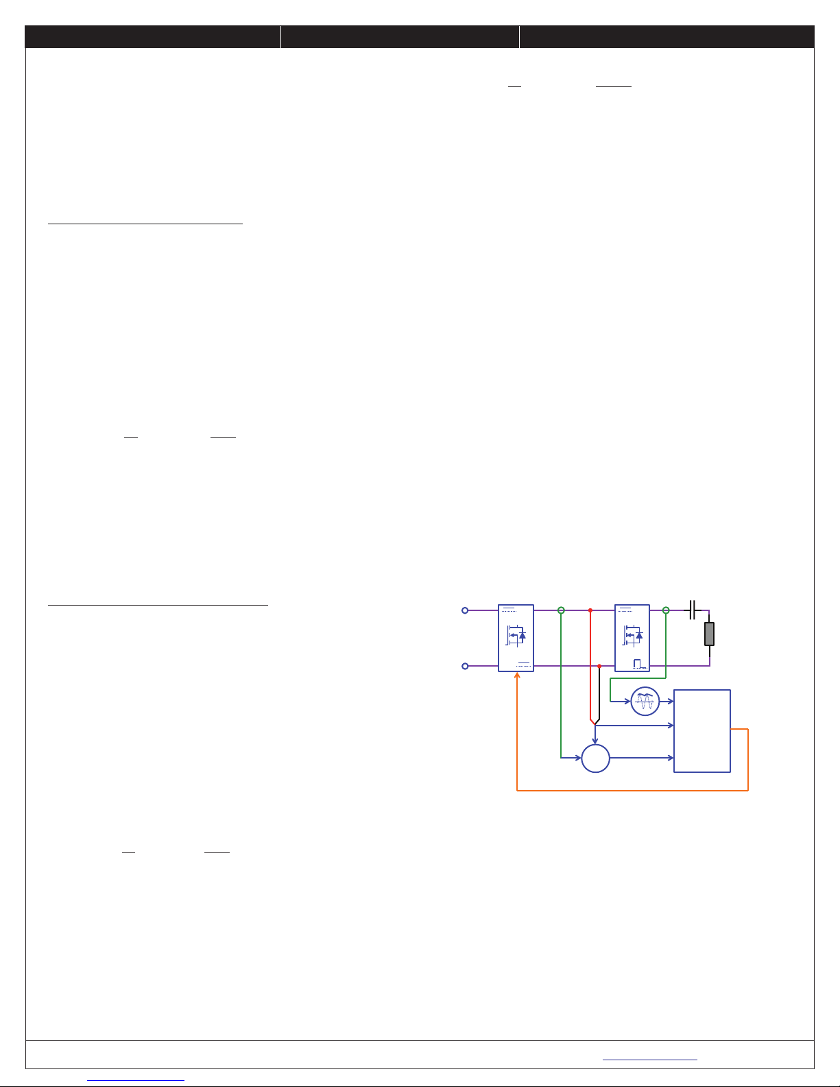
Demonstration System EPC9509
The pre-regulator can also be disabled in a similar manner as the oscillator
using JP50. However, note that this connection is oating with respect to the
ground so removing the jumper for external connection requires a oating
switch to correctly control this function. Refer to the datasheet of the con-
troller IC and the schematic in this QSG for specic details.
The ZVS timing adjust circuits for the ZVS class D ampliers are each
independently settable to ensure highest possible eciency setting and
includes separate ZVS tank circuits. This allows OOK modulation capability
for the amplier.
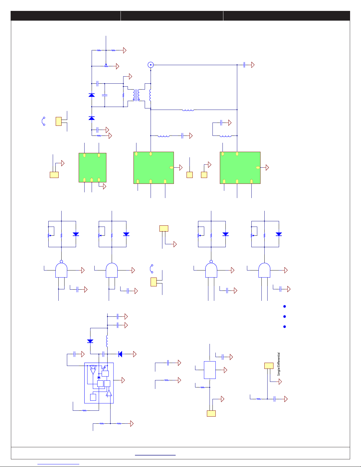
The EPC9509 is provided with 3 LED’s that indicate the mode of operation
of the system. If the system is operating in coil current limit mode, then the
green LED will illuminate. For power limit mode, the yellow LED will illumi-
nate. Finally, when the pre-regulator reaches maximum output voltage the
red LED will illuminate indicating that the system is no longer A4WP compli-
ant as the load impedance is too high for the amplier to drive. When the
load impedance is too high to reach power limit or voltage limit mode, then
the current limit LED will illuminate incorrectly indicating current limit mode.
This mode also falls outside the A4WP standard and by measuring the am-
plier supply voltage across TP1 and TP2 will show that it has nearly reach
the maximum value limit.
Single ended or Dierential Mode operation
The EPC9509 amplier can be operated in one of two modes; single-
ended or dierential mode. Single ended operation oers higher amplier
eciency but reduced imaginary impedance drive capability. If the
reected impedance of the tuned coil load exceeds the capability of
the amplier to deliver the desired power, then the amplier can be
switched over to dierential mode. In dierential mode, the amplier is
capable of driving an impedance range of 1 Ω through 56 Ω and ±50j Ω and
maintains either the 800 mARMS coil current or deliver up to 16 W of power.
The EPC9509 is set by default to dierential mode and can be switched to
single ended mode by inserting a jumper into J75. When inserted the ampli-
er operates in the single-ended mode. Using an external pull down with
oating collector/ drain connection will have the same eect. The external
transistor must be capable of sinking 25 mA and withstand at least 6 V.
For dierential mode only operation, the two ZVS inductors LZVS1 and LZVS2
can be replaced by a single inductor LZVS12 and by removing CZVS1 and CZVS2.
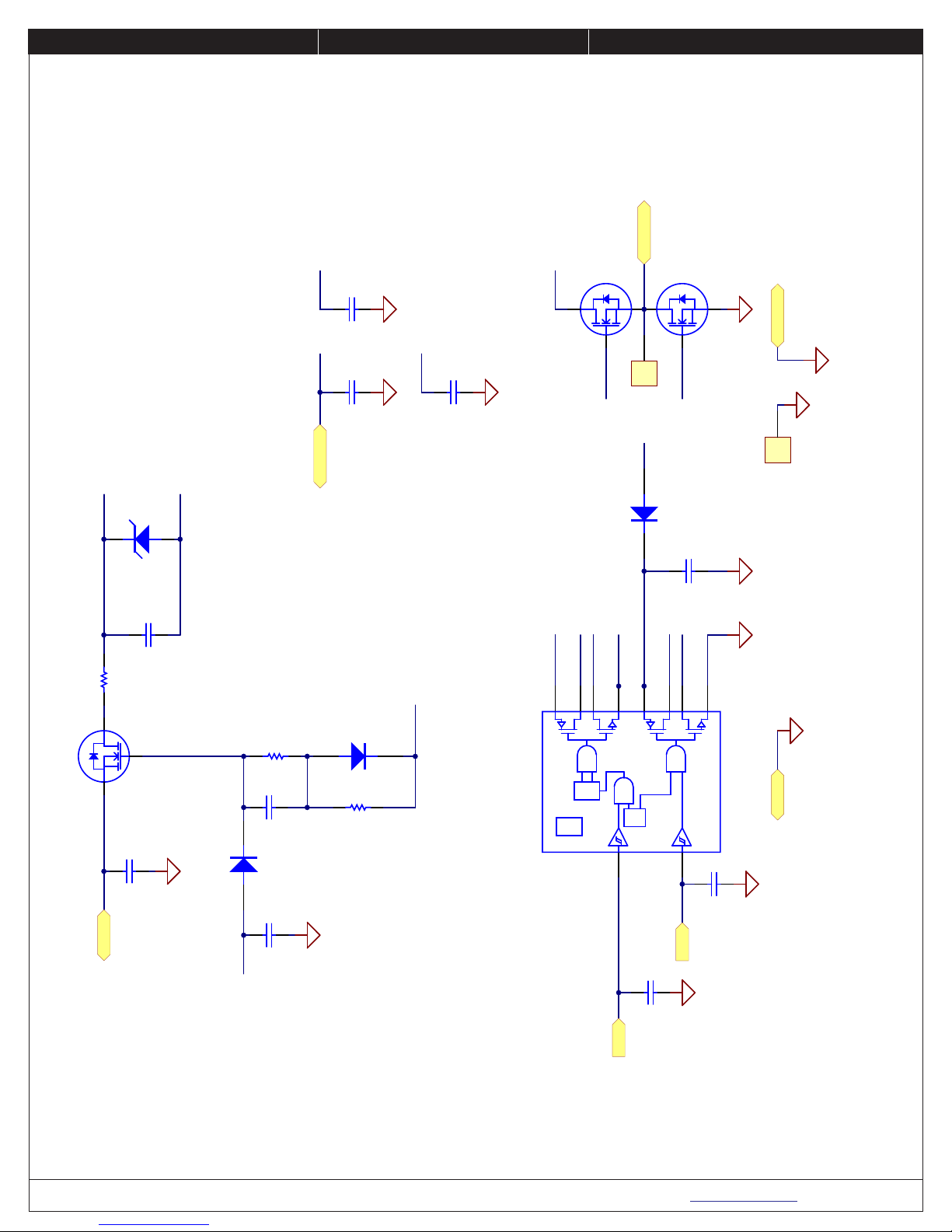
ZVS Timing Adjustment
Setting the correct time to establish ZVS transitions is critical to
achieving high eciency with the EPC9509 amplier. This can be
done by selecting the values for R71, R72, R77, and R78 or P71, P72,
P77, and P78 respectively. This procedure is best performed using a
potentiometer installed at the appropriate locations that is used to
determine the xed resistor values. The procedure is the same for both
single-ended and dierential mode of operation. The timing MUST
initially be set WITHOUT the source coil connected to the amplier.
The timing diagrams are given in Figure 5 and should be referenced when
following this procedure. Only perform these steps if changes have been
made to the board as it is shipped preset. The steps are:
1. With power o, remove the jumper in JP1 and install it into JP50 to place
the EPC9509 amplier into Bypass mode. Connect the main input power
supply (+) to JP1 (bottom pin – for bypass mode) with ground connected
to J1 ground (-) connection.
2. With power o, connect the control input power supply bus (19 V) to (+)
connector (J1). Note the polarity of the supply connector.
3. Connect a LOW capacitance oscilloscope probe to the probe-hole of
the half-bridge to be set and lean against the ground post as shown in
Figure 4.
4. Turn on the control supply – make sure the supply is approximately 19 V.
5. Turn on the main supply voltage starting at 0 V and increasing to the re-
quired predominant operating value (such as 24 V but NEVER exceed the
absolute maximum voltage of 52 V).
6. While observing the oscilloscope adjust the applicable potentiometers to
so achieve the green waveform of gure 5.
7. Repeat for the other half-bridge.
8. Replace the potentiometers with xed value resistors if required. Remove
the jumper from JP50 and install it back into JP1 to revert the EPC9509
back to pre-regulator mode.
Determining component values for LZVS
The ZVS tank circuit is not operated at resonance, and only provides the
necessary negative device current for self-commutation of the output
voltage at turn o. The capacitors CZVS1 and CZVS2 are chosen to have a
very small ripple voltage component and are typically around 1 µF. The
amplier supply voltage, switch-node transition time will determine the
value of inductance for LZVSx which needs to be sucient to maintain
ZVS operation over the DC device load resistance range and coupling
between the device and source coil range and can be calculated using
the following equation:
(1)
Where:
Δtvt = Voltage Transition Time [s]
ƒSW = Operating Frequency [Hz]
COSSQ = Charge Equivalent Device Output Capacitance [F]
Cwell = Gate driver well capacitance [F]. Use 20 pF for the LM5113
NOTE. that the amplier supply voltage VAMP is absent from the equation as
it is accounted for by the voltage transition time. The COSS of the EPC2108
eGaN FETs is very low and lower than the gate driver well capacitance Cwell
which as a result must now be included in the ZVS timing calculation.
The charge equivalent capacitance can be determined using the following
equation:
(2)
To add additional immunity margin for shifts in coil impedance, the
value of LZVS can be decreased to increase the current at turn o
of the devices (which will increase device losses). Typical voltage
transition times range from 2ns through 12ns. For the
dierential case the voltage and charge (COSSQ) are doubled when
calculating the ZVS inductance.
LZVS = ∆tvt
8 ∙ fsw∙ COSSQ + Cwell
COSSQ =
VAMP
∙
∫
0
VAMP
COSS (v) ∙ dv
1