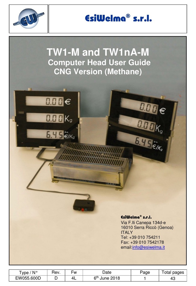
Epson/Seiko S5U1C63002P User manual

MF1017-02
CMOS 4-BIT SINGLE CHIP MICROCOMPUTER
(Peripheral Circuit Board for S1C63158/63358)
S5U1C63002P
Manual

NOTICE
No part of this material may be reproduced or duplicated in any form or by any means without the written permission of Seiko
Epson. Seiko Epson reserves the right to make changes to this material without notice. Seiko Epson does not assume any
liability of any kind arising out of any inaccuracies contained in this material or due to its application or use in any product or
circuit and, further, there is no representation that this material is applicable to products requiring high level reliability, such
as medical products. Moreover, no license to any intellectual property rights is granted by implication or otherwise, and there
is no representation or warranty that anything made in accordance with this material will be free from any patent or copyright
infringement of a third party. This material or portions thereof may contain technology or the subject relating to strategic
products under the control of the Foreign Exchange and Foreign Trade Law of Japan and may require an export license from
the Ministry of International Trade and Industry or other approval from another government agency.
© SEIKO EPSON CORPORATION 2001 All rights reserved.

The information of the product number change
Configuration of product number
Devices
Comparison table between new and previous number
S1C63 Family processors
Starting April 1, 2001, the product number will be changed as listed below. To order from April 1,
2001 please use the new product number. For further information, please contact Epson sales
representative.
S1 C63158 F0A01
Packing specification
Specification
Package (D: die form; F: QFP)
Model number
Model name (C: microcomputer, digital products)
Product classification (S1: semiconductor)
Development tools
S5U1 C63000 A1 1
Packing specification
Version (1: Version 1 ∗2)
Tool type (A1: Assembler Package ∗1)
Corresponding model number
(63000: common to S1C63 Family)
Tool classification (C: microcomputer use)
Product classification
(S5U1: development tool for semiconductor products)
∗1: For details about tool types, see the tables below. (In some manuals, tool types are represented by one digit.)
∗2: Actual versions are not written in the manuals.
Previous No.
E0C63158
E0C63256
E0C63358
E0C63P366
E0C63404
E0C63406
E0C63408
E0C63F408
E0C63454
E0C63455
E0C63458
E0C63466
E0C63P466
New No.
S1C63158
S1C63256
S1C63358
S1C6P366
S1C63404
S1C63406
S1C63408
S1C6F408
S1C63454
S1C63455
S1C63458
S1C63466
S1C6P466
S1C63 Family peripheral products
Previous No.
E0C63467
E0C63557
E0C63558
E0C63567
E0C63F567
E0C63658
E0C63666
E0C63F666
E0C63A08
E0C63B07
E0C63B08
E0C63B58
New No.
S1C63467
S1C63557
S1C63558
S1C63567
S1C6F567
S1C63658
S1C63666
S1C6F666
S1C63A08
S1C63B07
S1C63B08
S1C63B58
Previous No.
E0C5250
E0C5251
New No.
S1C05250
S1C05251
Comparison table between new and previous number of development tools
Development tools for the S1C63 Family Development tools for the S1C63/88 Family
Previous No.
ADP63366
ADP63466
ASM63
GAM63001
ICE63
PRC63001
PRC63002
PRC63004
PRC63005
PRC63006
PRC63007
URS63366
New No.
S5U1C63366X
S5U1C63466X
S5U1C63000A
S5U1C63000G
S5U1C63000H1
S5U1C63001P
S5U1C63002P
S5U1C63004P
S5U1C63005P
S5U1C63006P
S5U1C63007P
S5U1C63366Y
Previous No.
ADS00002
GWH00002
URM00002
New No.
S5U1C88000X1
S5U1C88000W2
S5U1C88000W1
00
00


S5U1C63002P MANUAL EPSON i
(PERIPHERAL CIRCUIT BOARD FOR S1C63158/63358)
CONTENTS
S5U1C63002P Manual (Peripheral Circuit Board for S1C63158/63358)
This manual describes how to use the S1C63 Family Peripheral Circuit Board (S5U1C63002P). This circuit
board is used to provide emulation functions when it is installed in the ICE (S5U1C63000H1), a debug-
ging tool for the 4-bit Single Chip Microcomputer S1C63 Family.
For details on ICE functions and how to operate the debugger, refer to the separately prepared manuals.
Contents
CHAPTER 1INTRODUCTION ____________________________________________ 1
1.1 Outline of S5U1C63002P .............................................................................1
1.2 Components of S5U1C63002P .....................................................................1
1.3 External View of S5U1C63002P ................................................................... 1
CHAPTER 2INSTALLING S5U1C63002P _________________________________ 2
2.1 Installing the S5U1C63002P in the ICE (S5U1C63000H1) ........................ 2
CHAPTER 3PRECAUTIONS ON USING THE S5U1C63002P
PERIPHERAL CIRCUIT BOARD _________________________________ 3
3.1 Operation Precautions.................................................................................. 3
3.2 Differences from an Actual IC ...................................................................... 3
CHAPTER 4NAME AND FUNCTION OF EACH PART ___________________________ 6
CHAPTER 5CONNECTING THE S5U1C63002P TO THE TARGET SYSTEM __________ 8
CHAPTER 6PRODUCT SPECIFICATIONS ___________________________________ 10


CHAPTER 1: INTRODUCTION
S5U1C63002P MANUAL EPSON 1
(PERIPHERAL CIRCUIT BOARD FOR S1C63158/63358)
CHAPTER 1INTRODUCTION
1.1 Outline of S5U1C63002P
The S5U1C63002P provides on a board all the peripheral circuits of S1C63 Family microcomputers other
than the core CPU. By installing this board in the ICE (S5U1C63000H1) you can use it to emulate each
model in the S1C63 Family. For the models that can be supported by this board, refer to "Precautions on
Using the S5U1C63002P Peripheral Circuit Board" included in this package.
Note that this board can be set to your intended model by loading mask option data (generated by
"FOG63XXX" software tool) into the ICE using the debugger command.
1.2 Components of S5U1C63002P
After unpacking your S5U1C63002P package, check to see that all of the following components are included.
(1) S5U1C63002P main unit (S5U1C63002P board, S5U1C63003P board) ............... 1 pair
(2) I/O cable (80-pin+40-pin/40-pin ×2 flat type)....................................................... 1 pair
(3) Target system I/O connector (40-pin) ...................................................................... 2 pcs.
(4) S5U1C63002P Manual (Peripheral Circuit Board for S1C63158/63358)............. 1 copy
(5) Warranty card ............................................................................................................... 1 card
(6) User registration card .................................................................................................. 1 card
(7) Precautions on Using the S5U1C63002P Peripheral Circuit Board ..................... 1 sheet
1.3 ExternalView of S5U1C63002P
VLCD(V2V/V3V)
OSC3(CR)Adj
OSC1(CR)Adj
VSVD
VCCHG VDC
OSCCDBONVDSELSVDS0SVDS2SVDONLPWR
CLKCHGHLONSVDS1SVDS3
RESET
GND
fOSC1(CR)
fOSC3(CR)
SEIKO EPSON CORP.
VADSEL
Fig. 1.3.1 External view of S5U1C63002P
PRC63003 REV.1
SEIKO EPSON CORP.
Fig. 1.3.2 External view of S5U1C63003P
∗The name 'PRC63003' on the development tool is the old
name of the product.

CHAPTER 2: INSTALLING S5U1C63002P
2EPSON S5U1C63002P MANUAL
(PERIPHERAL CIRCUIT BOARD FOR S1C63158/63358)
•Installing the Peripheral Circuit Board
Set the jig included with the ICE into position as
shown below. Using this jig as a lever, push it
toward the inside of the board evenly on the left
and right sides. After confirming that the
Peripheral Circuit Board has been firmly fitted
into the internal slot of the ICE, remove the jig.
•Dismounting the Peripheral Circuit Board
Set the jig included with the ICE into position as
shown below. Using this jig as a lever, push it
toward the outside of the board evenly on the
left and right sides. After confirming that the
Peripheral Circuit Board has been dismounted
from the backboard connector, pull the Periph-
eral Circuit Board out of the ICE.
Peripheral Circuit Board
Peripheral Circuit Board
Fig. 2.1.2 Installing the Peripheral Circuit Board
Fig. 2.1.3 Dismounting the Peripheral Circuit Board
CHAPTER 2INSTALLING S5U1C63002P
2.1 Installing the S5U1C63002P in the ICE (S5U1C63000H1)
(1) Unfasten the screws located on the left and right sides of the front panel of the ICE by turning them
counterclockwise, then remove the front panel.
(2) Insert the S5U1C63002P board into the ICE along the 2nd guide rails (lower slot) until the tip of the board
touches the back of the ICE. If some other board is mounted on the guide rails, remove that board by using
the jig supplied with the ICE before you insert the S5U1C63002P board (see Figure 2.1.3).
(3) Once the S5U1C63002P board has been inserted almost fully into the ICE, secure it in position by
using the jig supplied with the ICE (see Figure 2.1.2).
(4) In a similar fashion to Step (2), insert the S5U1C63003P board into the ICE along the uppermost guide
rails (upper slot).
(5) In a similar fashion to Step (3), secure it in position.
(6) When the above is done, replace the front panel.
(2) (3)
(4)
S5U1C63003P Board
S5U1C63002P Board
(5)
(1), (6)
Fig. 2.1.1 Installing the S5U1C63002P board in the ICE

CHAPTER 3: PRECAUTIONS ON USING THE S5U1C63002P PERIPHERAL CIRCUIT BOARD
S5U1C63002P MANUAL EPSON 3
(PERIPHERAL CIRCUIT BOARD FOR S1C63158/63358)
CHAPTER 3
P
RECAUTIONS
ON
U
SING
THE
S5U1C63002P
P
ERIPHERAL
C
IRCUIT
B
OARD
Follow the precautions described below to ensure that your S5U1C63002P board is used properly. Note,
however, that some functions described here may not be available with some models. For details, refer to
the technical hardware manual for each model.
3.1 Operation Precautions
(1) Always be sure to power off all connected equipment before connecting or disconnecting the cable.
(2) Do not turn the power on and do not load any mask option data while the input ports (K00–K03) are
all set to low level. It may cause a simultaneous key input reset.
3.2 Differences from an Actual IC
The S5U1C63002P emulation board differs in terms of functionality and characteristics from an actual IC,
a fact with requires your attention. If these differences are ignored, there is a possibility that your circuit
will not operate properly on an actual IC even though it might have performed well on the ICE.
(1)Difference in I/O
<Interface voltage>
The interface voltage between the S5U1C63002P board and the target system is fixed at +5 V. There-
fore, if your emulation requires using the same interface voltage as that of an actual IC, add a level
shifter circuit or some other appropriate circuit to the target system to satisfy this requirement.
<Output port drive capability>
The drive capability of each output port on the S5U1C63002P board is somewhat higher than that of
an actual IC. Check the drive capacity of each output terminal on the model by referring to its techni-
cal hardware manual before you design the system and software.
<Protective diode at each port>
The S5U1C63002P board contains VDD and VSS protective diodes at all I/O ports and the interface
voltage with the target is fixed at +5 V. Therefore, you cannot set the output ports on the
S5U1C63002P board for open-drain output and interface them with a voltage level exceeding VDD.
<Pull-up resistance>
The pull-up resistors on the S5U1C63002P board are fixed to a resistance value of about 220 kΩwhich
is different from that of an actual IC. Consult the technical hardware manual to check the pull-up
resistance of the actual IC.
When turning input terminals high with pull-up resistors, note that there is a difference in the time it
takes to set up the high level. For example, if you configure a key matrix circuit using a combination
of output and input ports, and pull the configuration high with pull-up resistors at the input ports, a
difference may result in a rise time delay.
(2)Difference in current consumption
Current consumption in the S5U1C63002P board greatly differs from that in an actual IC. Check the
LEDs on the S5U1C63002P board to estimate the approximate current consumption of the board. The
following lists the items that greatly affect the amount of current consumption:
- Those that can be estimated by checking LEDs and monitor pins
a) Run and Halt execution ratio (check the LED on the ICE)
b) CPU operating voltage switching circuit (VDC)
c) OSC3 oscillation ON/OFF circuit (OSCC)
d) CPU clock switching circuit (CLKCHG)
e) Voltage doubler ON/OFF circuit (DBON)

CHAPTER 3: PRECAUTIONS ON USING THE S5U1C63002P PERIPHERAL CIRCUIT BOARD
4EPSON S5U1C63002P MANUAL
(PERIPHERAL CIRCUIT BOARD FOR S1C63158/63358)
f) Voltage halver ON/OFF circuit (HLON)
g) Oscillation system voltage regulator power supply select circuit (VDSEL)
h) A/D converter power supply select circuit (VADSEL)
i) SVD ON/OFF circuit (SVDON)
j) LCD power supply ON/OFF circuit (LPWR)
k) LCD constant-voltage switching circuit (VCCHG)
- Those that require attention during system and software design
l) Currents consumed by internal pull-up resistors
m) Input ports in a floating state
(3)Functional difference
<LCD power supply circuit>
- There is a delay between the time the LCD power supply circuit (LPWR) is turned on and the time the
LCD drive waveform is output. This delay on the S5U1C63002P board is set to 107 msec. The delay on
an actual IC is different, however. Consult the technical hardware manual.
- Turning the LPWR register off in the external power mode stops outputting the LCD drive waveform.
At this time, the output voltage of this board is different from the actual IC as shown below.
1/2 bias 1/3 bias
SEG terminal
COM terminal
Actual IC
V
SS
V
C1
, V
C2
S5U1C63002P
V
C3
V
C1
, V
C2
SEG terminal
COM terminal
Actual IC
V
C1
V
C1
S5U1C63002P
V
C2
V
C1
<LCD drive waveform>
Pay attention when using this board for the model that can control static drive waveform output,
because the output waveform is different from the actual IC. (Only for 1/3 bias with V
SS
, V
C1
, V
C2
, V
C3
.)
V
C3
V
C2
V
C1
V
SS
V
C3
V
C2
V
C1
V
SS
V
C3
V
C2
V
C1
V
SS
V
C3
V
C2
V
C1
V
SS
<Actual IC>
<This board, LCD board>
SEG
terminal
COM
terminal
SEG
terminal
COM
terminal
Segment
register
10
<SVD circuit>
- Some models have a built-in SVD circuit that detects the voltage supplied from outside the terminal,
but this Peripheral Circuit Board cannot directly detect the supply voltage. The SVD function is
evaluated by artificially changing the power-supply voltage using the VSVD control on the
S5U1C63002P board.
- There is a delay between the time the power to the SVD circuit is turned on and the time the SVD data
is detected. This delay on the S5U1C63002P board is set to between 61 and 92 µsec. For the delay on an
actual IC, consult the technical hardware manual to ensure that there is a sufficient delay before the
output voltage is detected.

CHAPTER 3: PRECAUTIONS ON USING THE S5U1C63002P PERIPHERAL CIRCUIT BOARD
S5U1C63002P MANUAL EPSON 5
(PERIPHERAL CIRCUIT BOARD FOR S1C63158/63358)
<Oscillator circuit>
- There must be a waiting period between the time the OSC3 oscillation control circuit (OSCC) is turned
on and the moment at which oscillation stabilizes. The oscillator on the S5U1C63002P board can
operate when it is switched to OSC3 without the insertion of a waiting period. Therefore, consult the
technical hardware manual to set an appropriate waiting period on the actual IC.
- Separate instructions should be used to switch the clock from OSC3 to OSC1, and to stop the OSC3
circuit from oscillating. If these operations are performed simultaneously by one instruction, care
should be exercised. Although such operations are performed normally on the S5U1C63002P board,
an actual IC may not perform correctly.
- When using an external clock, make sure that it is adjusted for an amplitude of 5 V ±5% and for a
duty cycle of within 50% ±10%, and that it is input from the I/O connectors OSC1 and OSC3 with VSS
set for GND.
- Since the logic level on the S5U1C63002P board is high, its oscillation starting and oscillation stopping
times are different from those of an actual IC.
- The S5U1C63002P board contains oscillators for the OSC1 and OSC3. If the OSC3 oscillator is not used
on an actual IC, care should be exercised because operations are performed on the emulation board by
using its OSC3 circuit.
- In the S5U1C63002P, the ceramic and crystal oscillation frequencies of the OSC3 oscillation circuit are
fixed at 4 MHz.
<Access to undefined address space>
If undefined address space in the ROM or RAM is accessed for read or write, the read or written
values become indeterminate. Furthermore, since the way these values become indeterminate is
different in the S5U1C63002P board and an in actual IC, care should be exercised. Note that the ICE
has a function to cause program execution to break when access to an undefined address space is
attempted.
<Reset circuit>
- The S5U1C63002P board does not contain an oscillation stop detection circuit (to generate a system
reset signal when the oscillation has stopped). Note that the oscillation stop detection circuit does not
guarantee operation with 100% accuracy.
- The sequence of operations from when the ICE is powered on until the program starts operating is
different in the S5U1C63002P board and an actual IC. The ICE enters a ready state when the user
program, etc., as well as option data are loaded on the S5U1C63002P board.
<Internal power supply circuit>
- For VDC, DBON, HLON, VDSEL, and VADSEL, the S5U1C63002P board only contains registers and
does not actually control the voltages. Therefore, consult the technical hardware manual to set the
exact voltages. Furthermore, if the operating voltage (e.g., VDC) is switched over, consult the techni-
cal hardware manual to set a waiting period for stabilization.
- Although the S5U1C63002P board has a control (VLCD) to adjust the LCD drive voltage, an actual IC
in almost all cases does not have such an adjustment facility; therefore, be careful.
- The operating frequency range that can be used depends on the internal power-supply voltage.
Therefore, consult the technical hardware manual to ensure that your system will not be operated
with an improper combination of operating frequency and internal power-supply voltage.
<Analog comparator circuit>
Characteristics of the analog comparator circuit on the S5U1C63002P such as response time are
different from an actual IC. Consult the technical hardware manual for the analog comparator charac-
teristics to design the system and software.

CHAPTER 4: NAME AND FUNCTION OF EACH PART
6EPSON S5U1C63002P MANUAL
(PERIPHERAL CIRCUIT BOARD FOR S1C63158/63358)
CHAPTER 4NAME AND FUNCTION OF EACH PART
This chapter describes the name and function of each part of the S5U1C63002P board.
VLCD(V2V/V3V)
OSC3(CR)Adj
OSC1(CR)Adj
VSVD
VCCHG VDC
OSCCDBONVDSELSVDS0SVDS2SVDONLPWR
RESET
GND
fOSC1(CR)
fOSC3(CR)
SEIKO EPSON CORP.
CLKCHGHLONSVDS1SVDS3 VADSEL
(3)
(2) (7)
(4)
(5) (6)
(1)
Fig. 4.1 Top view of the S5U1C63002P board
(1)RESET switch
This switch resets the internal circuits of the S5U1C63002P board, and supplies a reset signal to the
ICE.
(2)Register monitor LED
The LED lights up when the corresponding register contains logic 1 and goes out when the register
contains logic 0.
(3)Register monitor pin
The pin is driven high when the corresponding register contains logic 1 and driven low when the
register contains logic 0.
No.
1
2
3
4
Name
VDC
OSCC
CLKCHG
DBON
No.
5
6
7
8
Name
HLON
VDSEL
VADSEL
SVD0
No.
9
10
11
12
Name
SVD1
SVD2
SVD3
SVDON
No.
13
14
15
16
Name
Unused
LPWR
VCCHG
Unused
(4)CR oscillation frequency monitor pin
This pin allows you to monitor on an oscilloscope the clock waveform generated by the CR oscillation
circuit. Output on this pin is always active regardless of how the oscillation circuit is controlled.
Name
GND
fOSC1 (CR)
fOSC3 (CR)
Function
Ground (VSS)
OSC1 CR oscillation clock
OSC3 CR oscillation clock

CHAPTER 4: NAME AND FUNCTION OF EACH PART
S5U1C63002P MANUAL EPSON 7
(PERIPHERAL CIRCUIT BOARD FOR S1C63158/63358)
(5)VSVD control
This control artificially changes the power-supply voltage to check whether the power-supply voltage
detection function is working properly.
Note that in a model that can detect 16 voltage levels, one position on this control indicates two
voltage values. The set power-supply voltages increase when the control is turned clockwise and
decrease when the control is turned counterclockwise.
SVD level 01234 567
8 9 10 11 12 13 14 15
(For example, SVD levels 0 and 8 fall on the same control position.)
(6)VLCD control
This control is used to adjust the LCD power supply voltage. Note, however, that an actual IC in
almost all cases has its LCD drive voltage fixed; therefore, be careful with the LCD drive voltage. The
LCD display becomes dark when the control is turned clockwise and becomes light when the control
is turned counterclockwise.
(7)CR oscillation frequency adjusting control
When you choose a CR oscillator on the S5U1C63002P board, you can use this control to adjust the CR
oscillation frequency by using a screwdriver, etc. The adjustment range is approx. 30 kHz to 190 kHz
for the OSC1, and approx. 190 kHz to 2.6 MHz for the OSC3. Note that not all actual ICs operate in
this frequency range. Therefore, consult the technical hardware manual to ensure that the oscillation
frequency is adjusted within the stipulated frequency range. The oscillation frequency increases when
the control is turned clockwise and decreases when the control is turned counterclockwise.

CHAPTER 5: CONNECTING THE S5U1C63002P TO THE TARGET SYSTEM
8EPSON S5U1C63002P MANUAL
(PERIPHERAL CIRCUIT BOARD FOR S1C63158/63358)
CHAPTER 5CONNECTING THE S5U1C63002P
TO THE TARGET SYSTEM
This chapter describes how to connect the S5U1C63002P board to the target system.
To connect the S5U1C63002P board to the target system, use the I/O connection cable (80-pin+40-pin/40-
pin ×2, flat type) included with this package. Handle with this connector carefully as the power (VDD) is
supplied through this connector.
mark
To target board
CN1-2
(40-pin)
S5U1C63002P board
(80-pin)
To target board
CN1-1
(40-pin)
mark
I/O connection cable
S5U1C63003P board
(40-pin)
Fig. 5.1 Connecting the S5U1C63002P to the target system

CHAPTER 5: CONNECTING THE S5U1C63002P TO THE TARGET SYSTEM
S5U1C63002P MANUAL EPSON 9
(PERIPHERAL CIRCUIT BOARD FOR S1C63158/63358)
Table 5.1 I/O connector pin assignment
No.
1
2
3
4
5
6
7
8
9
10
11
12
13
14
15
16
17
18
19
20
21
22
23
24
25
26
27
28
29
30
31
32
33
34
35
36
37
38
39
40
40-pin CN1-1 connector
Pin name
V
DD
V
DD
K00
K01
K02
K03
K10
K11
K12
K13
V
SS
V
SS
P00
P01
P02
P03
P10
P11
P12
P13
V
DD
V
DD
P20
P21
P22
P23
P30
P31
P32
P33
V
SS
V
SS
P40
P41
P42
P43
V
REF
K20
V
SS
V
SS
Pin function
Power supply (+)
Power supply (+)
K00 port
K01 port
K02 port
K03 port
K10 port
K11 port
K12 port
K13 port
Power supply (–)
Power supply (–)
P00 port
P01 port
P02 port
P03 port
P10 port
P11 port
P12 port
P13 port
Power supply (+)
Power supply (+)
P20 port
P21 port
P22 port
P23 port
P30 port
P31 port
P32 port
P33 port
Power supply (–)
Power supply (–)
P40 port
P41 port
P42 port
P43 port
A/D converter reference voltage input
K20 port
Power supply (–)
Power supply (–)
No.
1
2
3
4
5
6
7
8
9
10
11
12
13
14
15
16
17
18
19
20
21
22
23
24
25
26
27
28
29
30
31
32
33
34
35
36
37
38
39
40
40-pin CN1-2 connector
Pin name
V
DD
V
DD
R00
R01
R02
R03
R10
R11
R12
R13
V
SS
V
SS
R20
R21
R22
R23
R30
R31
R32
R33
V
DD
V
DD
BZ
–
–
–
–
ECLK1
–
ECLK3
V
SS
V
SS
V
C1
V
C2
V
C3
V
C4
V
C5
RESET
V
SS
V
SS
Pin function
Power supply (+)
Power supply (+)
R00 port
R01 port
R02 port
R03 port
R10 port
R11 port
R12 port
R13 port
Power supply (–)
Power supply (–)
R20 port
R21 port
R22 port
R23 port
R30 port
R31 port
R32 port
R33 port
Power supply (+)
Power supply (+)
Buzzer output
Cannot be connected
Cannot be connected
Cannot be connected
Cannot be connected
External clock input (OSC1)
Cannot be connected
External clock input (OSC3)
Power supply (–)
Power supply (–)
V
C1
power supply
V
C2
power supply
V
C3
power supply
V
C4
power supply
V
C5
power supply
System reset input
Power supply (–)
Power supply (–)
Note that some pin names are not existed in the actual IC depending on the model.

CHAPTER 6: PRODUCT SPECIFICATIONS
10 EPSON S5U1C63002P MANUAL
(PERIPHERAL CIRCUIT BOARD FOR S1C63158/63358)
CHAPTER 6PRODUCT SPECIFICATIONS
The components specifications of the S5U1C63002P are listed below.
S5U1C63002P
Dimension: 254 mm (wide) ×144.8 mm (depth) ×13 mm (height) (including screws)
Weight: Approx. 180 g
Power supply: DC 5 V ± 5%, less than 1 A (supplied from ICE main unit)
S5U1C63003P
Dimension: 254 mm (wide) ×144.8 mm (depth) ×13 mm (height) (including screws)
Weight: Approx. 150 g
Power supply: DC 5 V ± 5%, less than 0.7 A (supplied from ICE main unit)
I/O connection cable
S5U1C63002P connector: KEL8830E-80-170LD
S5U1C63003P connector: 3M3432-5002LCSC
Cable connector (80-pin): KEL8822E-80-171
Cable connector (40-pin): 3M7940-6500SC 1 pair
Cable: 40-pin flat cable 1 pair
Interface: CMOS interface (5 V)
Length: Approx. 40 cm
Accessories
40-pin connector for connecting to target system:
3M3432-6002LCSC ×2

AMERICA
EPSON ELECTRONICS AMERICA, INC.
- HEADQUARTERS -
1960 E. Grand Avenue
EI Segundo, CA 90245, U.S.A.
Phone: +1-310-955-5300 Fax: +1-310-955-5400
- SALES OFFICES -
West
150 River Oaks Parkway
San Jose, CA 95134, U.S.A.
Phone: +1-408-922-0200 Fax: +1-408-922-0238
Central
101 Virginia Street, Suite 290
Crystal Lake, IL 60014, U.S.A.
Phone: +1-815-455-7630 Fax: +1-815-455-7633
Northeast
301 Edgewater Place, Suite 120
Wakefield, MA 01880, U.S.A.
Phone: +1-781-246-3600 Fax: +1-781-246-5443
Southeast
3010 Royal Blvd. South, Suite 170
Alpharetta, GA 30005, U.S.A.
Phone: +1-877-EEA-0020 Fax: +1-770-777-2637
EUROPE
EPSON EUROPE ELECTRONICS GmbH
- HEADQUARTERS -
Riesstrasse 15
80992 Munich, GERMANY
Phone: +49-(0)89-14005-0 Fax: +49-(0)89-14005-110
SALES OFFICE
Altstadtstrasse 176
51379 Leverkusen, GERMANY
Phone: +49-(0)2171-5045-0 Fax: +49-(0)2171-5045-10
UK BRANCH OFFICE
Unit 2.4, Doncastle House, Doncastle Road
Bracknell, Berkshire RG12 8PE, ENGLAND
Phone: +44-(0)1344-381700 Fax: +44-(0)1344-381701
FRENCH BRANCH OFFICE
1 Avenue de l' Atlantique, LP 915 Les Conquerants
Z.A. de Courtaboeuf 2, F-91976 Les Ulis Cedex, FRANCE
Phone: +33-(0)1-64862350 Fax: +33-(0)1-64862355
BARCELONA BRANCH OFFICE
Barcelona Design Center
Edificio Prima Sant Cugat
Avda. Alcalde Barrils num. 64-68
E-08190 Sant Cugat del Vallès, SPAIN
Phone: +34-93-544-2490 Fax: +34-93-544-2491
ASIA
EPSON (CHINA) CO., LTD.
28F, Beijing Silver Tower 2# North RD DongSanHuan
ChaoYang District, Beijing, CHINA
Phone: 64106655 Fax: 64107319
SHANGHAI BRANCH
4F, Bldg., 27, No. 69, Gui Jing Road
Caohejing, Shanghai, CHINA
Phone: 21-6485-5552 Fax: 21-6485-0775
EPSON HONG KONG LTD.
20/F., Harbour Centre, 25 Harbour Road
Wanchai, Hong Kong
Phone: +852-2585-4600 Fax: +852-2827-4346
Telex: 65542 EPSCO HX
EPSON TAIWAN TECHNOLOGY & TRADING LTD.
10F, No. 287, Nanking East Road, Sec. 3
Taipei
Phone: 02-2717-7360 Fax: 02-2712-9164
Telex: 24444 EPSONTB
HSINCHU OFFICE
13F-3, No. 295, Kuang-Fu Road, Sec. 2
HsinChu 300
Phone: 03-573-9900 Fax: 03-573-9169
EPSON SINGAPORE PTE., LTD.
No. 1 Temasek Avenue, #36-00
Millenia Tower, SINGAPORE 039192
Phone: +65-337-7911 Fax: +65-334-2716
SEIKO EPSON CORPORATION KOREA OFFICE
50F, KLI 63 Bldg., 60 Yoido-dong
Youngdeungpo-Ku, Seoul, 150-763, KOREA
Phone: 02-784-6027 Fax: 02-767-3677
SEIKO EPSON CORPORATION
ELECTRONIC DEVICES MARKETING DIVISION
Electronic Device Marketing Department
IC Marketing & Engineering Group
421-8, Hino, Hino-shi, Tokyo 191-8501, JAPAN
Phone: +81-(0)42-587-5816 Fax: +81-(0)42-587-5624
ED International Marketing Department Europe & U.S.A.
421-8, Hino, Hino-shi, Tokyo 191-8501, JAPAN
Phone: +81-(0)42-587-5812 Fax: +81-(0)42-587-5564
ED International Marketing Department Asia
421-8, Hino, Hino-shi, Tokyo 191-8501, JAPAN
Phone: +81-(0)42-587-5814 Fax: +81-(0)42-587-5110
International Sales Operations

http://www.epson.co.jp/device/
(Peripheral Circuit Board for S1C63158/63358)
S5U1C63002P Manual
EPSON Electronic Devices Website
ELECTRONIC DEVICES MARKETING DIVISION
First issue October, 1997
Printed February, 2001 in Japan A
M
Table of contents
Popular Computer Hardware manuals by other brands
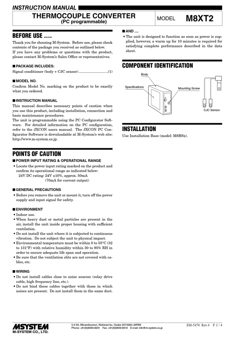
M-system
M-system M8XT2 instruction manual

Tri-M Systems
Tri-M Systems REB 2000 Series Faq
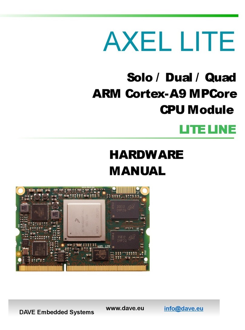
Dave Embedded Systems
Dave Embedded Systems AXEL LITE Hardware manual

GRASS VALLEY
GRASS VALLEY M848-9005-491 Installation & quick start guide

SMK-Link
SMK-Link VP6495 user manual
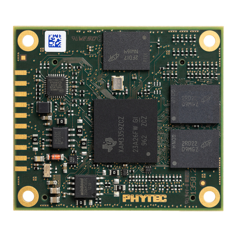
Phytec
Phytec phyCORE-AM335 Series Hardware manual
Bitspower
Bitspower BPTA-O11DTE-V2-HA installation guide

ST
ST STEVAL-OET005 user manual
Renesas
Renesas YRBRL78G14 quick start guide
Texas Instruments
Texas Instruments LDC3114-Q1 manual
Western Digital
Western Digital WD Serial ATA RAID Controller Quick install guide
GIGAIPC
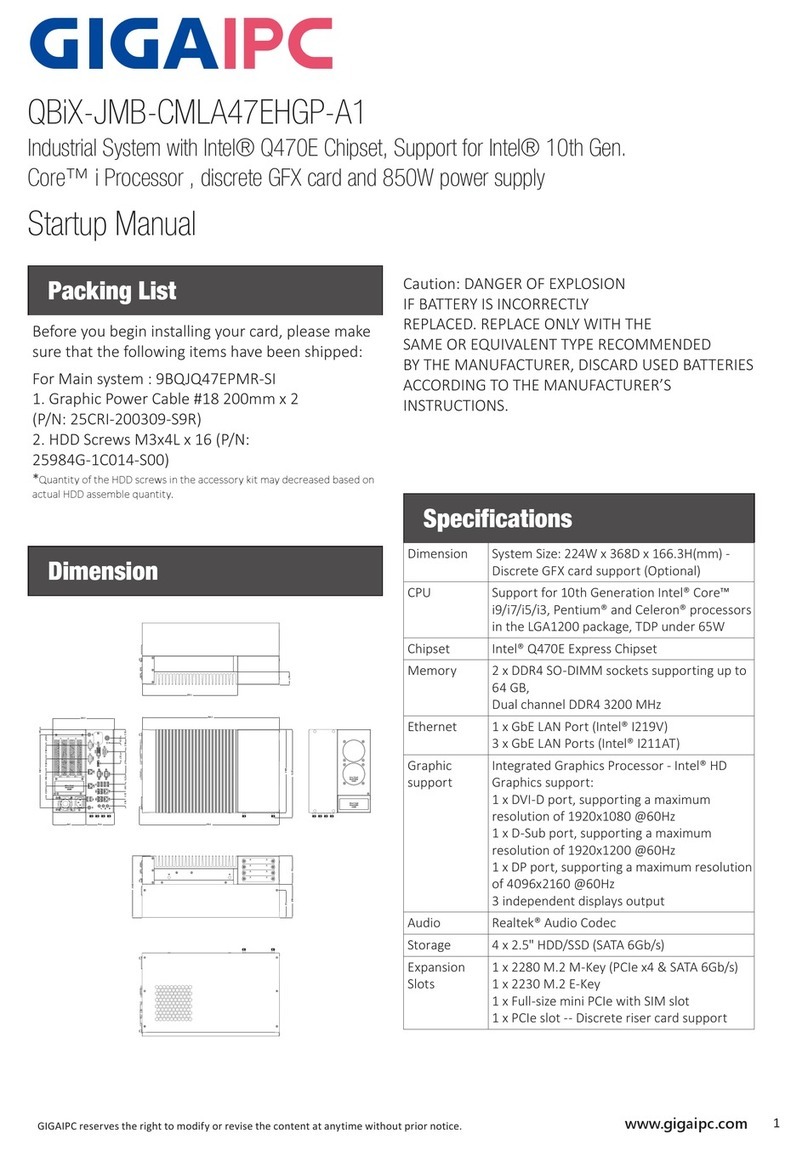
GIGAIPC QBiX-JMB-CMLA47EHGP-A1 Startup manual

