Exar XRT83SL38/L38EVAL User manual

XRT83SL38/L38EVAL User Manual
Page 1 of 23
XRT83SL38/L38EVAL
EVALUATION SYSTEM
USER MANUAL

XRT83SL38/L38EVAL User Manual
Page 2 of 23
EVALUATION KIT PART LIST
This kit contains the following:
• XRT83SL38/L38EVAL Application Board
• XRT83SL38/L38 GUI Evaluation Software
• XRT83SL38/L38 128-Pin TQFP
• XRT83SL38/L38EVAL User Manual
• XRT83SL38/L38 Datasheet
FEATURES
• CPLD Design Which Emulates Microprocessor Support for the 8-Bit Parallel Interface
• 25 DIN Connector for Easy Connection Through a Standard Parallel Port to a PC
• CD ROM or Floppy Disk Containing the GUI Software (Executable File)
• Line Interface Modules Coupled to the Receiver Inputs and Transmitter Outputs
• Power Supply Design Allowing a Single 3V Supply voltage
• Accessible I/O Interface for Common Laboratory Equipment
• Optimized layout with Four Layers
INTRODUCTION
The XRT83SL38/L38EVAL is a complete printed circuit board for characterizing Exar’s
XRT83SL38/L38. The XRT83SL38/L38 is a fully integrated four channel, long haul, short haul
line interface unit for T1, E1 or J1 applications.
This application board combines a proven PC board layout with optimized analog and digital
interface circuitry. The XRT83SL38/L38EVAL contains the device being tested, CPLD for
emulating microprocessor support for the 8-bit parallel interface, line interface modules coupled to
the receiver inputs and transmitter outputs, and I/O headers for a flexible user interface.
Complete AC and DC performance of the XRT83SL38/L38 can be evaluated by interfacing
external laboratory equipment.
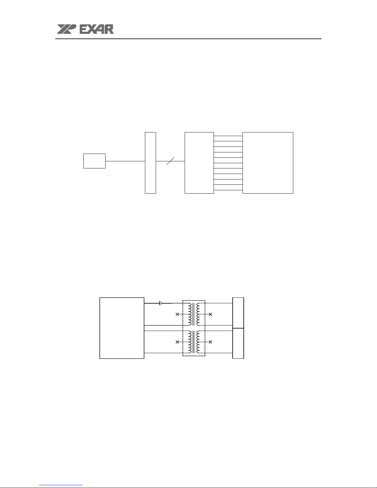
SYSTEM CONFIGURATION-LAB SETUP
The XRT83SL38/L38EVAL application board is setup as a common test circuit. Figure 1 shows a
simplified block diagram of the default test configuration.
PC
25 DIN Connector
A[7:0]
D[7:0]
INT
PCLK
RDY
RD
WR
CS
HW/HOSTB
RST
ALE
CPLD
XRT83SL38
XRT83L38
LIU
TTIP[7:0]
TRING[7:0]
RTIP[7:0]
RRING[7:0]
ConnectorConnector
XRT83SL38/L38 PCB
Parallel Port Cable
TPOS[7:0]
TCLK[7:0]
RPOS[7:0]
RNEG[7:0]
RCLK[7:0]
TNEG[7:0]
ConnectorConnector
5
Figure 1 Simplified Block Diagram of the XRT83SL38/L38EVAL Application Board
XRT83SL38/L38EVAL User Manual
Page 3 of 23
APPLICATION CIRCUITRY
CPLD
The XRT83SL38/L38EVAL uses a CPLD designed to emulate a microprocessor support module
for an 8-Bit parallel interface. Using Exar’s GUI software (included in the evaluation kit), the
XRT83SL38/L38EVAL can be controlled through a standard parallel port cable connected to a
PC. The GUI was written to simplify the evaluation process of Exar’s LIU. Access to all the
control registers and functionality fo all four channels is available. For information on the GUI
software, see the “XRT83SL38/L38EVAL GUI SOFTWARE” section of this manual. Figure 2 is a
simplified block diagram of the CPLD interface. CPLD
XRT83SL38
XRT83L38
LIU
25 DIN Connector
5
Parallel Port Cable
A[7:0]
D[7:0]
INT
PCLK
ALE
RST
HW/HOSTB
CS
WR
RD
RDY
PC
Figure 2 Simplified Block Diagram of the CPLD Interface
Line Interface Module
Internal Impedance Mode
The XRT83SL38/L38 has an internal and external impedance mode. For internal impedance
mode, no termination resistors are necessary for the transmit outputs. This allows the user to
have one bill of materials for all three applications. Figure 3 is a simplified block diagram of the
internal impedance mode. For external impedance mode, see the following sections for the
resistor values chosen for the corresponding application.
Line Interface Module
TTIP
TRING
RTIP
RRING
XRT83SL38/L38 LIU
0.47uF
Figure 3 Simplified Block Diagram of the Internal Impedance Mode
XRT83SL38/L38EVAL User Manual
Page 4 of 23
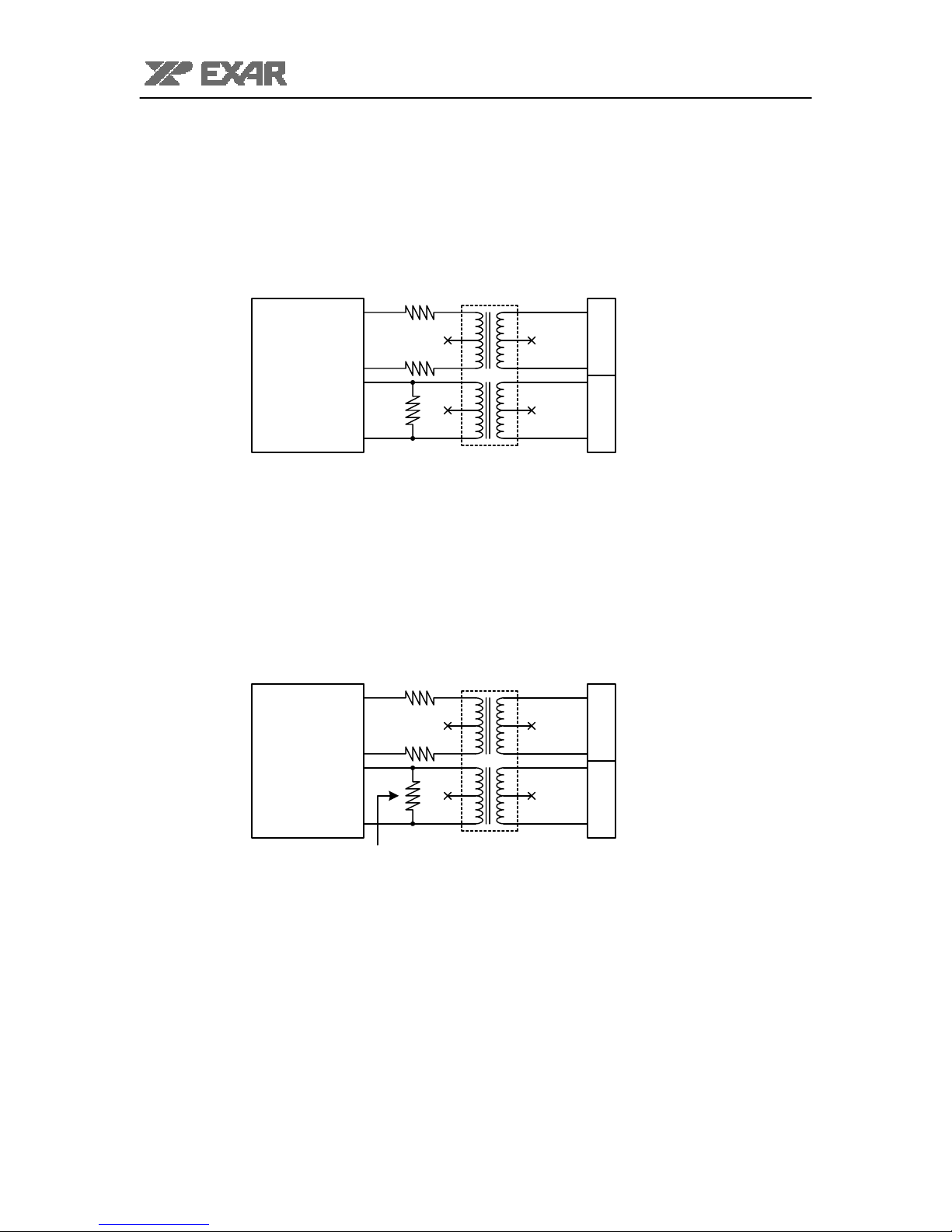
External Impedance Mode (T1/J1, 1.544MHz, 100ohm/110ohm)
The XRT83SL38/L38EVAL can be programmed for external impedance mode through the
microprocessor interface. For T1 applications, two 3.1ohm resistors are necessary on the
transmit outputs of the LIU. A 100ohm resistor is necessary on the receiver inputs. (Note: These
values do not change when using either a 1:2 or 1:2.45 turns ratio on the transmit side) Figure 4
is a simplified block diagram of the external mode for T1 applications.
3.1
3.1
Line Interface Module
TTIP
TRING
RTIP
RRING
XRT83SL38/L38 LIU
100
1:2
1:1
Figure 4 Simplified Block Diagram of the External Mode, T1/J1
External Impedance Mode (E1, 2.048MHz, 75ohm or 120ohm)
The XRT83SL38/L38EVAL can be programmed for external impedance mode through the
microprocessor interface. For E1 applications, two 9.1ohm resistors are necessary on the
transmit outputs of the LIU. A 75ohm or 120ohm resistor is necessary on the receiver inputs.
(Note: The resistor values on the transmit side change to 6.2ohms when using a 1:2.45 turns
ratio) Figure 5 is a simplified block diagram of the external mode for E1 applications.
9.1
9.1
Line Interface Module
TTIP
TRING
RTIP
RRING
75 (for 75ohm Termination)
120 (for 120ohm Termination)
XRT83SL38/L38 LIU
1:2
1:1
Figure 5 Simplified Block Diagram of the External Mode, E1 75ohm and 120ohm

XRT83SL38/L38EVAL User Manual
Page 5 of 23
3V_SUP
ICT
C4
0.1uF
TEST
TERSEL0
TAOS4
3V_AVDD
TAOS7
C5
0.1uF
TxON3
R13
36
CLKSEL2
XRT83SL38/L38 OCTAL LONG HAUL, SHORT HAUL LIU MAIN INTERFACE
3V_DVDD
TxTSEL
MCLKE1
CODES4
TERSEL0
TERSEL1
U5
2.048MHz
8
4
5VCC
GND
CLK
TAOS1
TAOS2
TP1
1T
TAOS0
U1A
XRT83SL38/L38
80
190
191
192
193
194
133
128
67
68
69
70
71
72
73
74
94
173
174
175
176
177
178
179
180
89
81
82
195
196
197
198
63
64
65
66
134
167
168
26
27
23
187
188
189
199
10
147
166
62
43
114
95
127
75
30 83
84
85
86
87
88
6
14
143
151
47
39
118
110
5
15
38
48
109
119
142
152
132
28
29
76
77
131
184
185
186
8
12
41
45
112
116
145
149
2
18
35
51
106
122
139
155
129
24
25
78
79
130
181
182
183
MODE
WR_EQC0
RD_EQC1
ALE_EQC2
CS_EQC3
RDY_EQC4
PTS1_RCLKE
PTS2_TCLKE
D7_LOOP14
D6_LOOP04
D5_LOOP15
D4_LOOP05
D3_LOOP16
D2_LOOP06
D1_LOOP17
D0_LOOP07
PCLK_ATAOS
A7_LOOP13
A6_LOOP03
A5_LOOP12
A4_LOOP02
A3_LOOP11
A2_LOOP01
A1_LOOP10
A0_LOOP00
RxMUTE
RxRES1
RxRES0
TAOS0
TAOS1
TAOS2
TAOS3
TAOS4
TAOS5
TAOS6
TAOS7
FIFOS
JASEL0
JASEL1
MCLKE1
MCLKT1
MCLKOUT
CLKSEL0
CLKSEL1
CLKSEL2
DMO0
DMO1
DMO2
DMO3
DMO4
DMO5
DMO6
DMO7
INT_TRATIO
RESET
SR/DR RxTSEL
TxTSEL
TERSEL1
TERSEL0
TEST
ICT
AGND
AGND
AGND
AGND
AGND
AGND
AGND
AGND
EXT_VCM
EXT_VCM
EXT_VCM
EXT_VCM
EXT_VCM
EXT_VCM
EXT_VCM
EXT_VCM
AGND
GNDPLL
GNDPLL
DGND
DGND
DGND
DGND
DGND
DGND
TVDD
TVDD
TVDD
TVDD
TVDD
TVDD
TVDD
TVDD
RVDD
RVDD
RVDD
RVDD
RVDD
RVDD
RVDD
RVDD
AVDD
VDDPLL
VDDPLL
DVDD
DVDD
DVDD
DVDD
DVDD
DVDD
C2
0.1uF
TAOS7
3V_SUP
SMB1
EXT CLOCK
TAOS2
CODES6
TERSEL1
TAOS4
MCLKT1
MCLKE1
U3
16.384MHz
8
4
5VCC
GND
CLK
TAOS3
TxON6
J3
1 2
++
R2
470 TAOS0
CLKSEL0
TxTSEL
R3
470
TxON4
3V_SUP
3V_RVDD
CODES0
TAOS3
TxON7
TxON5
P1
DB25
13
25
12
24
11
23
10
22
9
21
8
20
7
19
6
18
5
17
4
16
3
15
2
14
1
C3
0.1uF
RxTSEL
TEST
EXAR AD Infinitum
TxON2
TxON0
R4
470
TAOS5
TAOS6
U2
XC95144XL
40
39
35
34
112
111
110
107
7
9
44
45
142
140
105
104
71
69
66
68
70
4
126
41
43
46
121
124
113
33
31
28
27
26
25
24
23
135
134
133
132
131
130
129
128
106
103
101
102
14
15
16
19
17
125
120
119
118
117
116
22
21
20
115
136
137
138
139
10
11
12
13
65
67
63
122
30
32
38
5
6
2
3
143
18
29
36
47
62
72
89
90
99
108
114
123
144
8
42
84
141
1
37
55
73
109
127
TxON0
TxON1
TxON2
TxON3
TxON4
TxON5
TxON6
TxON7
CODES0
CODES1
CODES2
CODES3
CODES4
CODES5
CODES6
CODES7
SDO
SDI
SCK
SCS
SRST
SR/DR
RESET
JASEL1
JASEL0
FIFOS
RxRES0
RxRES1
RxMUTE
A7_LOOP13
A6_LOOP03
A5_LOOP12
A4_LOOP02
A3_LOOP11
A2_LOOP01
A1_LOOP10
A0_LOOP00
D7_LOOP14
D6_LOOP04
D5_LOOP15
D4_LOOP05
D3_LOOP16
D2_LOOP06
D1_LOOP17
D0_LOOP07
PCLK_ATAOS
INT_TRATIO
PTS1_RCLKE
PTS2_TCLKE
RDY_EQC4
CS_EQC3
ALE_EQC2
WR_EQC0
RD_EQC1
MODE
RxTSEL
TxTSEL
TERSEL1
TERSEL0
TEST
CLKSEL0
CLKSEL1
CLKSEL2
ICT
TAOS7
TAOS6
TAOS5
TAOS4
TAOS3
TAOS2
TAOS1
TAOS0
TMS
TCK
TDI
TDO
MCLK
GCK2
GCK3
GTS1
GTS2
GTS3
GTS4
GSR
GND
GND
GND
GND
GND
GND
GND
GND
GND
GND
GND
GND
GND
VCC
VCC
VCC
VCC
VCCIO
VCCIO
VCCIO
VCCIO
VCCIO
VCCIO
R9
4.7k
CODES2
R10
36 R11
4.7k
CODES7
CLKSEL1
CLKSEL2
TAOS5
H1
JTAG
1
3
5
2
4
6
+
+
+
+
+
+
R7
36
RxTSEL
3V_SUP
R1
10k
CLKSEL1
3V_RVDD
J1
1 2
++
R5
470
TAOS6
J2
1 2
++
TxON1
ICT
3V_SUP
XRT83SL38/L38 LONG HAUL, SHORT HAUL LIU D
XRT83SL38/L38
C
13Tuesday, September 17, 2002
Design File Name = H:\XRT LIU\XRT83L38\SCHEMATIC\XRT83L38 EVAL.DSN
Title
Size Document Number Rev
Date: Sheet of
CLKSEL0
MCLKT1
3V_SUP
R12
36
R8
OPEN
CODES5
CODES3
TAOS1
R6
4.7k
U4
1.544MHz
8
4
5VCC
GND
CLK
C1
0.1uF
CODES1
Figure 6 XRT83SL38/L38EVAL Schematic Page 1

XRT83SL38/L38EVAL User Manual
Page 6 of 23
RPOS2
R94 3.0
R51
OPEN
C34
0.1uF
S28
5
61
2
34
C25
0.1uF
3V_DVDD
T3
See Note 1
161
2
143
15
11
9
10
6
7
8
J6
RJ48
1
2
3
4
5
6
7
89
10
CODES1
S31
1 2
3 4
5 6
7 8
910
11 12
13 14
15 16
++
++
++
++
++
++
++
++
J5
1 2
++
S5
HEADER 4X2
1
2
3
45
6
7
8
RCLK2
S33
1 2
3 4
5 6
7 8
910
11 12
13 14
15 16
++
++
++
++
++
++
++
++
R126 0.0
R99 30.1
R105 3.0
+
C11
10uF
J14
1 2
++
D2
LED
R118 9.1
RPOS3
TxON3
RPOS2
TP5 1
T
T1
See Note 1
161
2
143
15
11
9
10
6
7
8
C24
0.1uF
C22
0.1uF
C13
0.1uF
3V_RVDD
ISOLATION2
RPOS0
S34
5
61
2
34
R110 30.1
R121 30.1
R98 18.7
C29
0.1uF
R112 3.0
RCLK2
R96 9.1
R93 0.0
J7
RJ48
1
2
3
4
5
6
7
89
10
M1
MHOLE
1
MH
D1
5.6V
2 1
T4
See Note 1
161
2
143
15
11
9
10
6
7
8
C30
0.1uF
MOUNTING HOLES
ISOLATION1
RPOS1
+
C15
10uF
R132 30.1
RCLK1
+
C28
OPEN
RCLK3
B2
GND
1
R129 9.1
R108 25.0
R101 3.0
R103 9.1
R91 6.2
BANNANA PLUGS
R117 6.2
3V_SUP
RCLK0
C26
0.1uF
CODES0
C12
0.1uF
TxON2
R104 0.0
S30
5
61
2
34
Tx=1:2, Rx=1:1
RCLK3
RNEG3
R95 6.2
S10
HEADER 4X2
1
2
3
45
6
7
8
RPOS0
R115 0.0
R125 9.1
R130 25.0
TP3 1
T
EXAR AD Infinitum
R97 25.0
TxON0
RNEG3
R106 6.2
M2
MHOLE
1
MH
U1B
XRT83SL38/L38
206
22
135
159
207
21
136
158
208
20
137
157
1
19
138
156
3
17
140
154
4
16
141
153
7
13
144
150
9
11
146
148
204
201
164
161
205
200
165
160
203
202
163
162
169
170
171
172
RLOS0
RLOS1
RLOS2
RLOS3
RCLK0
RCLK1
RCLK2
RCLK3
RNEG0_LCV0
RNEG1_LCV1
RNEG2_LCV2
RNEG3_LCV3
RPOS0
RPOS1
RPOS2
RPOS3
RTIP0
RTIP1
RTIP2
RTIP3
RRING0
RRING1
RRING2
RRING3
TTIP0
TTIP1
TTIP2
TTIP3
TRING0
TRING1
TRING2
TRING3
TPOS0
TPOS1
TPOS2
TPOS3
TNEG0_CODES0
TNEG1_CODES1
TNEG2_CODES2
TNEG3_CODES3
TCLK0
TCLK1
TCLK2
TCLK3
TxON0
TxON1
TxON2
TxON3
R109 18.7
TRANSPOWER SMD606-05
R120 18.7
R123 3.0
LIU TRANSMIT AND RECEIVE
C38
0.1uF
+
C16
10uF
RCLK0
TP4 1
T
S7
HEADER 4X2
1
2
3
45
6
7
8
R131 18.7
M4
MHOLE
1
MH
XRT83SL38/L38 LONG HAUL, SHORT HAUL LIU D
XRT83SL38/L38
C
23Tuesday, July 02, 2002
Design File Name = H:\XRT LIU\XRT83L38\SCHEMATIC\XRT83L38 EVAL.DSN
Title
Size Document Number Rev
Date: Sheet of
R107 9.1
J4
1 2
++
R90 3.0
C33
0.1uF
M3
MHOLE
1
MH
+
C31
10uF
R114 9.1
GROUND POINTS
TxON1
R127 3.0
CODES2
R124 6.2
RNEG2
S32
5
61
2
34
C37
0.1uF
R119 25.0
RCLK1
R113 6.2
R92 9.1
R102 6.2
R88
OPEN
R100 0.47uF
RNEG0
J8
RJ48
1
2
3
4
5
6
7
89
10
J9
RJ48
1
2
3
4
5
6
7
89
10
C32
0.1uF
RNEG0
C39
0.1uF
C23
0.1uF
HALO TG74-1505N1
RPOS1
RNEG1
S2
HEADER 4X2
1
2
3
45
6
7
8
B1
3V
1
POWER CIRCUITRY
T2
See Note 1
161
2
143
15
11
9
10
6
7
8S29
1 2
3 4
5 6
7 8
910
11 12
13 14
15 16
++
++
++
++
++
++
++
++
R122 0.47uF
+
C27
OPEN
R111 0.47uF
RNEG1
R116 3.0
Note 1: Transformer Selection
3V_AVDD
S27
1 2
3 4
5 6
7 8
910
11 12
13 14
15 16
++
++
++
++
++
++
++
++
C35
0.1uF
CODES3
R89 0.47uF
RPOS3
R14
470
RNEG2
C36
0.1uF
C14
0.1uF
R128 6.2
TP2 1
T
Figure 7 XRT83SL38/L38EVAL Schematic Page 2

XRT83SL38/L38EVAL User Manual
Page 7 of 23
T7
See Note 1
161
2
143
15
11
9
10
6
7
8
R165 30.1
R174 25.0
R149 3.0
S38
5
61
2
34
ISOLATION1
RNEG6
R133 0.47uF
R167 3.0
S18
HEADER 4X2
1
2
3
45
6
7
8
R138 3.0
R166 0.47uF
CODES5 R142 18.7
RPOS4
RPOS4
R164 18.7
R176 30.1
R175 18.7
S39
1 2
3 4
5 6
7 8
910
11 12
13 14
15 16
++
++
++
++
++
++
++
++
S40
5
61
2
34
S20
HEADER 4X2
1
2
3
45
6
7
8
T8
See Note 1
161
2
143
15
11
9
10
6
7
8
HALO TG74-1505N1
R150 6.2
R172 6.2
R156 3.0
TxON4
J11
RJ48
1
2
3
4
5
6
7
89
10
R162 9.1
TxON5
RPOS5
R145 3.0
RCLK4
R163 25.0
RNEG6
EXAR AD Infinitum
RPOS5
RPOS7
J10
RJ48
1
2
3
4
5
6
7
89
10
TxON6
S37
1 2
3 4
5 6
7 8
910
11 12
13 14
15 16
++
++
++
++
++
++
++
++
R135 6.2
S23
HEADER 4X2
1
2
3
45
6
7
8
RCLK7
R147 9.1
R137 0.0
RCLK4
S42
5
61
2
34
T6
See Note 1
161
2
143
15
11
9
10
6
7
8
R154 30.1
R155 0.47uF
R173 9.1
RCLK5
R143 30.1
R144 0.47uF
ISOLATION2
RNEG5
TxON7
RCLK7
R140 9.1
S41
1 2
3 4
5 6
7 8
910
11 12
13 14
15 16
++
++
++
++
++
++
++
++
RNEG5
RNEG7
S15
HEADER 4X2
1
2
3
45
6
7
8
R153 18.7
R170 0.0
R168 6.2
R146 6.2
R158 9.1
J12
RJ48
1
2
3
4
5
6
7
89
10
Tx=1:2, Rx=1:1
CODES4 U1C
XRT83SL38/L38
55
31
126
102
54
32
125
103
53
33
124
104
52
34
123
105
50
36
121
107
49
37
120
108
46
40
117
111
44
42
115
113
57
60
97
100
56
61
96
101
58
59
98
99
90
91
92
93
RLOS4
RLOS5
RLOS6
RLOS7
RCLK4
RCLK5
RCLK6
RCLK7
RNEG4_LCV4
RNEG5_LCV5
RNEG6_LCV6
RNEG7_LCV7
RPOS4
RPOS5
RPOS6
RPOS7
RTIP4
RTIP5
RTIP6
RTIP7
RRING4
RRING5
RRING6
RRING7
TTIP4
TTIP5
TTIP6
TTIP7
TRING4
TRING5
TRING6
TRING7
TPOS4
TPOS5
TPOS6
TPOS7
TNEG4_CODES4
TNEG5_CODES5
TNEG6_CODES6
TNEG7_CODES7
TCLK4
TCLK5
TCLK6
TCLK7
TxON4
TxON5
TxON6
TxON7
R141 25.0
CODES7
RNEG4
R148 0.0
CODES6
RCLK5
RNEG7
R136 9.1
RPOS7
RCLK6
R169 9.1
RPOS6
R171 3.0
J13
RJ48
1
2
3
4
5
6
7
89
10
T5
See Note 1
161
2
143
15
11
9
10
6
7
8
S36
5
61
2
34
S35
1 2
3 4
5 6
7 8
910
11 12
13 14
15 16
++
++
++
++
++
++
++
++
R157 6.2
R134 3.0
R161 6.2
RPOS6
RNEG4
R159 0.0
R139 6.2
RCLK6
R160 3.0
XRT83SL38/L38 LONG HAUL, SHORT HAUL LIU D
XRT83SL38/L38
C
33Tuesday, July 02, 2002
Design File Name = H:\XRT LIU\XRT83L38\SCHEMATIC\XRT83L38 EVAL.DSN
Title
Size Document Number Rev
Date: Sheet of
R152 25.0
LIU TRANSMIT AND RECEIVE
Note 1: Transformer Selection
TRANSPOWER SMD606-05
R151 9.1
Figure 8 XRT83SL38/L38EVAL Schematic Page 3
XRT83SL38/L38EVAL User Manual
Page 8 of 23
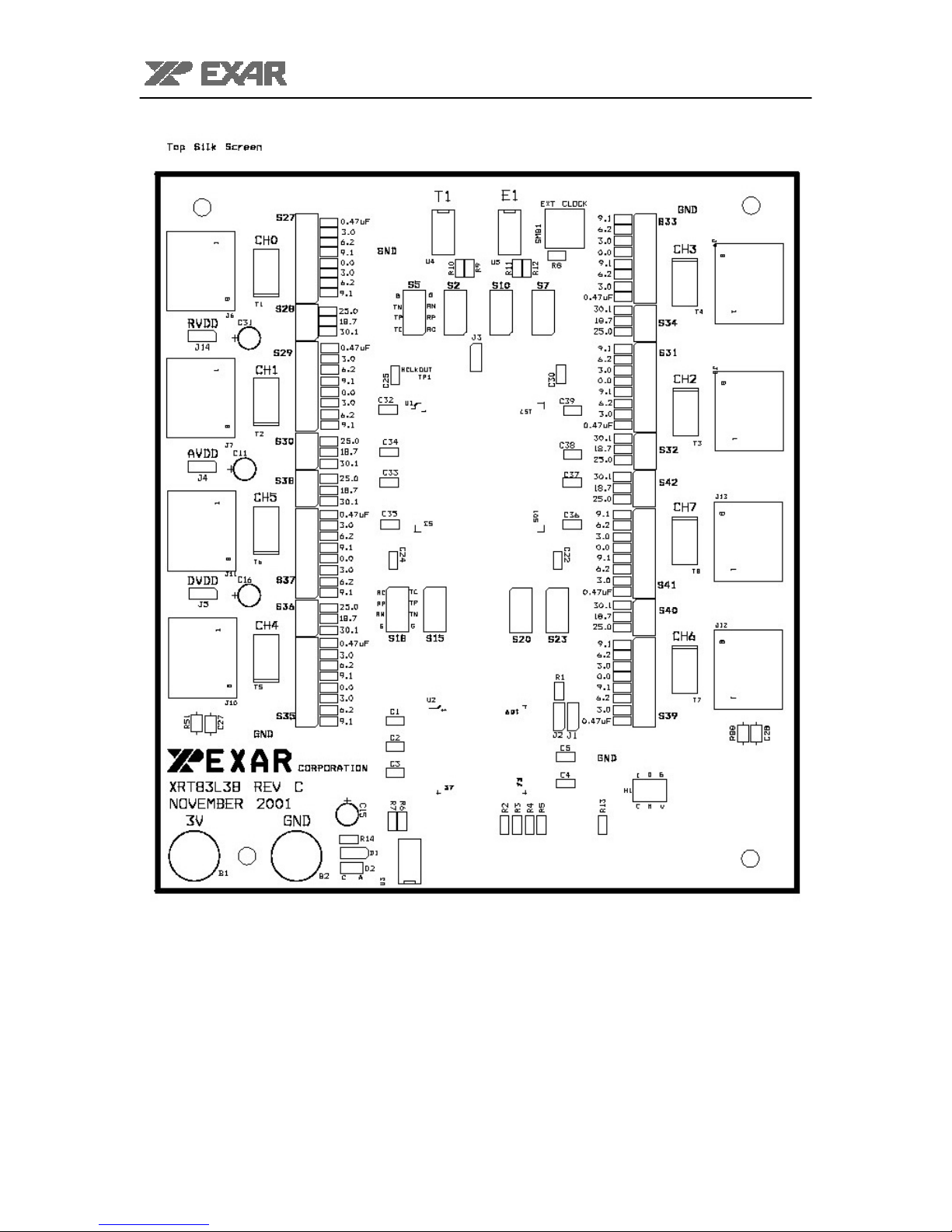
Figure 9 XRT83SL38/L38EVAL Layout Plot-Top Silk Screen
XRT83SL38/L38EVAL User Manual
Page 9 of 23
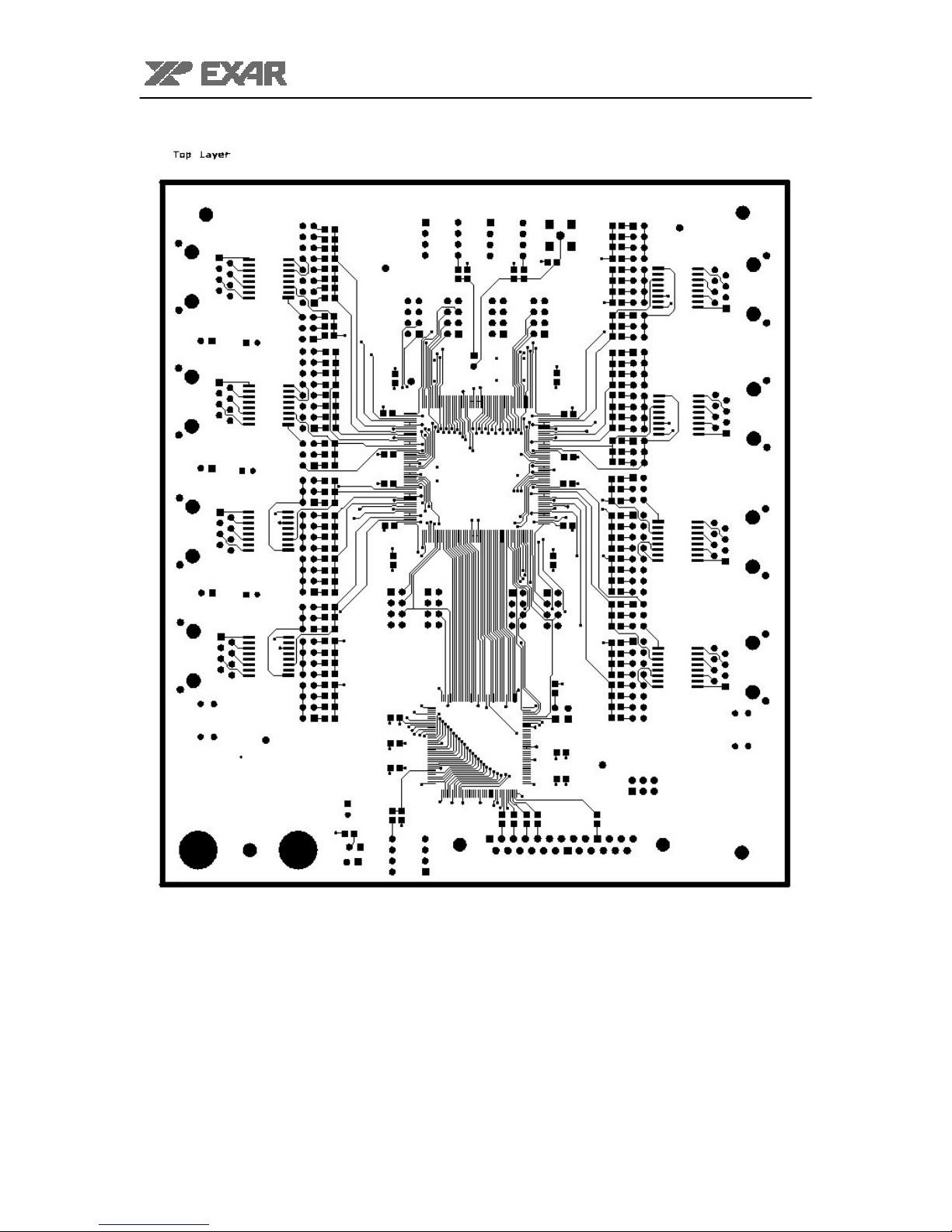
Figure 10 XRT83SL38/L38EVAL Layout Plot-Top Layer

XRT83SL38/L38EVAL User Manual
Page 10 of 23
Figure 11 XRT83SL38/L38EVAL Layout Plot-Ground Plane
XRT83SL38/L38EVAL User Manual
Page 11 of 23
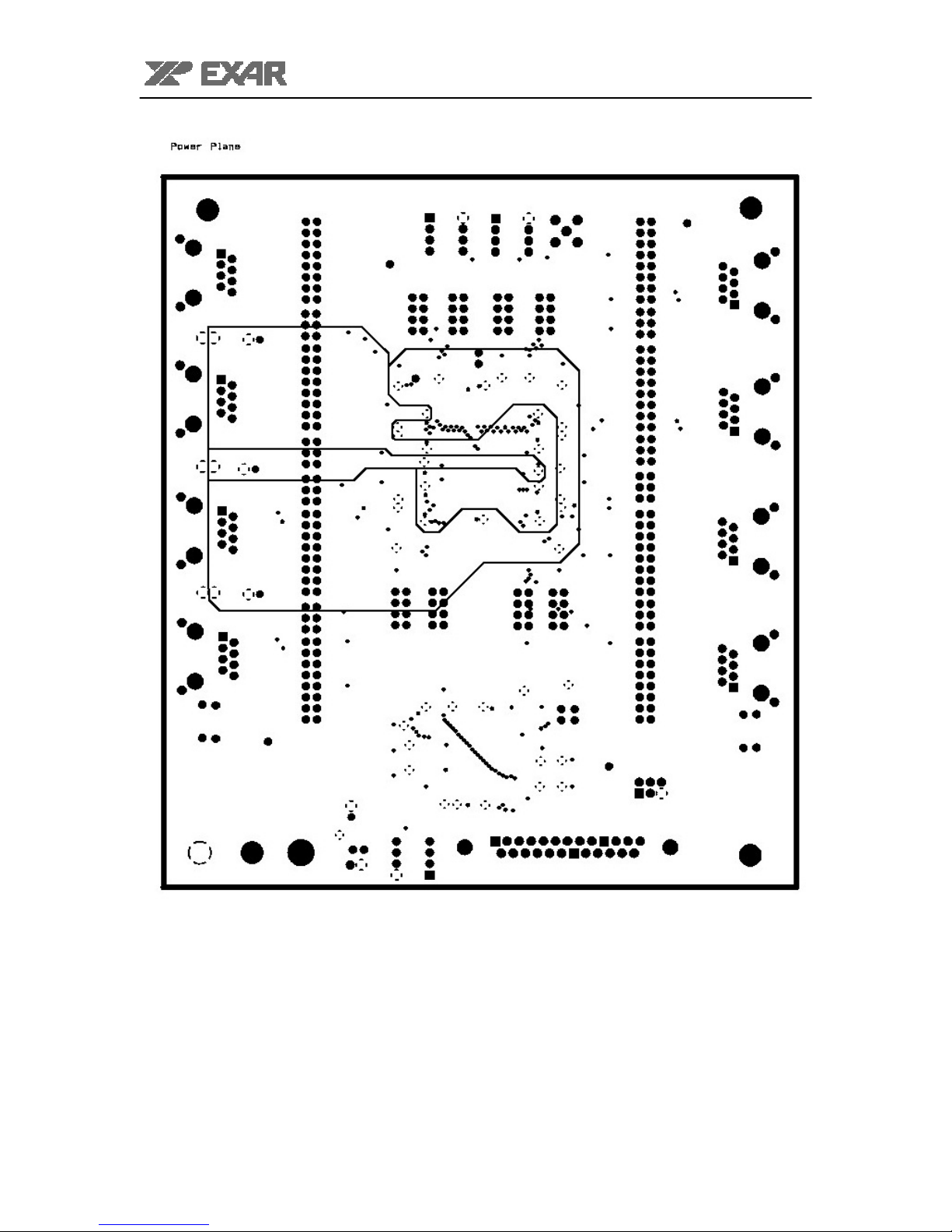
Figure 12 XRT83SL38/L38EVAL Layout Plot-Power Plane

XRT83SL38/L38EVAL User Manual
Page 12 of 23
Figure 13 XRT83SL38/L38EVAL Layout Plot-Bottom Layer

XRT83SL38/L38EVAL User Manual
Page 13 of 23
The XRT83SL38/L38 Evaluation Board GUI Software
The XRT83SL38/L38 Evaluation Board Kit comes with a floppy disk / CD ROM that contains a file
of the name: “xrt83SL38/L38vxx.exe”. This file is the executable code for the “XRT83SL38/L38
Evaluation Board GUI Software.
This section provides the reader with a thorough overview of the XRT83SL38/L38 Evaluation
Board GUI Software and all of its features.
Installing the XRT83SL38/L38 Evaluation Board GUI Software, on to the PC
Installing the “XRT83SL38/L38 Evaluation Board GUI Software, onto a PC is really quite simple.
All the user has to do is copy all the file from the floppy disk / CD ROM onto the hard-drive of the
PC (within the user’s directory of choice).
Connecting the XRT83SL38/L38 Evaluation Board to the PC
When the XRT83SL38/L38 Evaluation Board is operating in the “Host” Mode, the user will
exercise command and control over the Evaluation Board via a PC which is executing the
“XRT83SL38/L38 Evaluation Board GUI” Software. Prior to starting up and executing the GUI
Software, the user is required to connect the parallel port connector of the Evaluation Board to
the parallel-port of the PC, via a parallel-port cable. The “XRT83SL38/L38 Evaluation Board will
communicate with the XRT83SL38/L38 Evaluation Board hardware via this parallel-port cable.
Starting up the GUI Software
Once the executable file for the “XRT83SL38/L38 Evaluation Board GUI” Software has been
loaded into the “Host” PC, and Evaluation Board has been connected to the PC, via a parallel-
port cable, the user can execute the GUI software, by any of the normal “Window ‘95” means.
This can by “double-clicking” on the “xrt83SL38/L38.exe” filename or icon, or by going through
the “START” button.

XRT83SL38/L38EVAL User Manual
Page 14 of 23
The XRT83SL38/L38 Evaluation Board GUI Software Start Up Window
Shortly after the user has selected and started up the “XRT83SL38/L38 Evaluation Board GUI
Software, the PC monitor should be display the “Start-up” Window, as depicted below in Figure
14.
Figure 14, The “Start-Up” Window, within the XRT83SL38/L38 Evaluation Board GUI
Software
Figure 14 indicates that the “Start-Up” Window consists of a menu bar which contains the
following three “pull-down” menus:
• File
• Tests
• Help
Each of these “Pull-down” menus will be discussed in some detail below.

XRT83SL38/L38EVAL User Manual
Page 15 of 23
The File pull-down Menu
Figure 15 presents an illustration of the “Start-Up” window with the “File” pull-down menu fully
visible.
Figure 15, Illustration of the “File” Pull-down Menu
Figure 15 indicates that the “File” pull-down menu contains the following options:
“Port”
“Exit”
Each of these options are discussed in detail below
Port Setup
The “Port Setup” option permits the user to select the address where the parallel port is located.
The default address is 0x378. A check mark indicates which address it is currently set to.
Note: This section DOES NOT change your system configurations for the parallel port. This
option is needed ONLY when the address to your system’s parallel port is not set at 0x378.
Exit
The “Exit” option permits the user to “gracefully” terminate and exit the program.

XRT83SL38/L38EVAL User Manual
Page 16 of 23
The “Tests” pull-down Menu
Figure 16 presents an illustration of the “Start-up” window with the “Tests” pull-down menu fully
visible.
Figure 16, Illustration of the “Tests” Pull-down Menu
Figure 16 indicates that the “Tests” option only consists of the “Evaluation Board Test” option.
Once the user selects this option, then the “Host Mode” or “Hardware Mode” Dialog (depending
on the board configuration) will appear as illustrated below, see Figures 17 and 18.
XRT83SL38/L38EVAL User Manual
Page 17 of 23
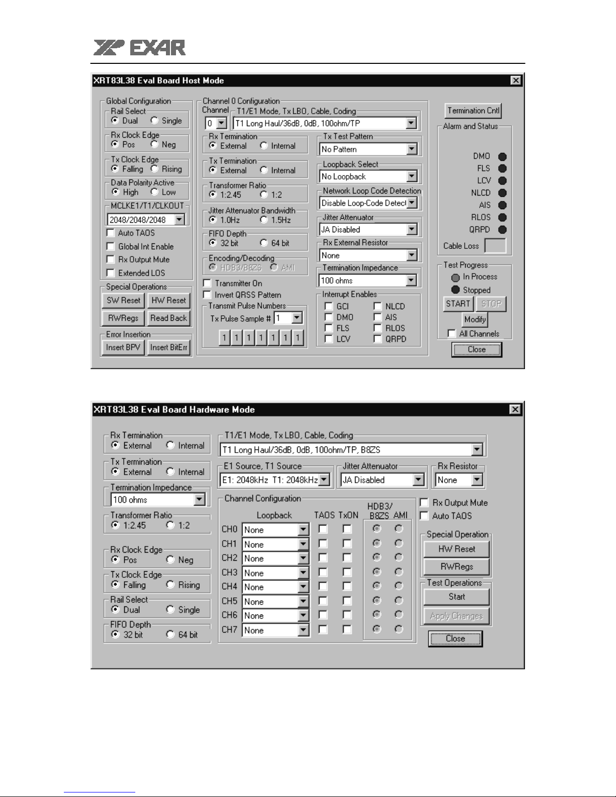
Figure 17, Illustration of Host Mode Test Dialog Box
Figure 18, Illustration of Host Mode Test Dialog Box

XRT83SL38/L38EVAL User Manual
Page 18 of 23
At this point, the user will be able to specify his/her configuration settings for the XRT83SL38/L38
device; and implement these settings. A more detailed discussion of the “Host Mode” and
“Hardware Mode” Dialogs is presented in the next section.
The “Help” pull-down Menu
Figure 19 presents an illustration of the “Start-up” window with the “Help” pull-down menu fully
visible.
Figure 19, Illustration of the “Help” Pull-down Menu
Figure 19 indicates that the “Help” option consists of two options.
•About XRT83L3x Eval Software
Host Mode Test
Figure 20 presents an illustration of the Host Mode Test Dialog Box. The GUI should display this
box under the following condition.
• In response to the selection of the “Evaluation Board Test” option within the “Test” pull-down
menu.

XRT83SL38/L38EVAL User Manual
Page 19 of 23
The Host Mode Test Dialog Box represents the main interface that the user will have to the
XRT83SL38/L38 Evaluation Board, via the GUI Software. All options that are offered by the
XRT83SL38/L38 device, when operating in the “Host” Mode, are offered via the “Host Mode Test
Dialog Box”. The following sections explain the options and features associated with the Host
Mode Test Dialog Box.
Figure 20, Illustration of the Host Mode Test Dialog Box
Figure 20 indicates that the Host Mode Test Dialog Box consists of the following sections
• Global Configurations
• Ch.1 (Ch.2, Ch.3, Ch.4, etc.) Channel Configuration
• Alarms and Status (Current Channel)
• Special Operations
• Error Insertion (Current Channel)
• Test Progress
Each of these sections is discussed in detail.

XRT83SL38/L38EVAL User Manual
Page 20 of 23
The Global Configuration Section
The “Global Configuration” Section of the Host Mode Test Dialog Box permits the user to do the
following. It is important to note settings in this section take effect only after either “START” or
“Modify” buttons are pressed.
• Rail Select, Select the Rail Select (Data Format) (i.e., Single Rail or Dual Rail)
• Rx Clock Edge, Select which edge of RCLK the output data of all channels is to be updated.
• Tx Clock Edge, Select which edge of TCLK the transmit data of all channels is to be sampled.
• Data Polarity Active, Select Data Polarity Active state to be high or low.
• MCLKE1/T1/CLKOUT, Select MCLKE1/T1/CLKOUT clock sources. A drop list box provides
all possible settings. For example the setting 1544/2048/1544 sets the E1 clock source to
1544 MHz, the T1 clock source to 2048 MHz and the master clock rate to 1544 MHz.
• Auto TAOS, Enable/disable Auto TAOS (i.e., Automatic Transmission of All Ones for all
channels)
• Global Int Enable, when checked enables interrupt generation for all channels.
• Rx Output Mute, mutes receive outputs of RPOS/RDATA and RNEG/LCV pins to a “0” state
for any channel that detects an RLOS condition.
• Extended LOS, when enabled the number of zeros at the receive input of each channel
before RLOS is declared to 4096 bits.
The Ch.1 to Ch.8 Channel Configuration Section
The “Ch.1 (Ch.2, Ch.3, Ch.4, etc.) Channel Options” Section of the Host Mode Test Dialog Box
permits the user to do the following. It is important to note settings in this section take effect only
after either “START” or “Modify” buttons are pressed and only for the current channel (unless All
Channels is checked).
• Rx Termination, selects between the internal and external line termination modes for the
receiver.
• Tx Termination, selects between the internal and external line termination modes for the
transmitter.
• Transformer Ratio, in external termination mode, this selects the transformer ratio for the
transmitter. In internal, the selection has no effect.
• Jiiter Attenuator Bandwidth, in E1 mode this setting allows the user to select the Jitter
Bandwidth. This setting has no effect for T1 mode.
• FIFO Depth, select the size of FIFO Depth for the current channel.
• Jitter Attenuator, used the place the Jitter Attenuator in Transmit/Receive Path or to disable it.
• Encoding/Decoding, selects en/decoding for current channel. Alternate Mark Inversion or
HDB3/B8ZS coding schemes can be selected. Setting active only in single rail mode.
• Transmitter On, checked to turn on the transmit section of the current channel. unchecked to
tri-state TTIP and TRING.
• Invert QRSS Pattern, setting inverts the polarity of transmitted QRSS pattern.
• Transmit Pulse Numbers, setting for the magnitude of transmit samples in a given transmit
period. The user sets the bits individually. The sample numbers are 7-bits long and the MSB
is leftmost.
• Tx Test Pattern, allows the user to choose a transmit test pattern. Choices are
Transmit/Detect Quasi-Random Signal, Transmit All Ones, Transmit Network Loop-Up Code,
Transmit Network Loop-Down Code, and No Pattern.
• Loopback Select, allows the user to select a loopback mode for the current channel. Choices
are No Loopback, Dual Loopback, Analog Loopback, and Digital Loopback.
• Network Loop Code Detection, setting is used to monitor the receive data and set the NLCD
bit when “00001” (Loop-Up) or “001” (Loop-down) is detected in the receive data for more
than 5 seconds. Automatic Loop-Code detection enables remote loopback activation and
looks for a Loop-Up code and once detected looks for a Loop-Down code. Upon Loop-Down,
the remote loopback is removed.
Table of contents
Other Exar Motherboard manuals

Exar
Exar XRA1403IL24-F User manual

Exar
Exar SP338 User manual

Exar
Exar XR20M1280 User manual

Exar
Exar SP336E User manual

Exar
Exar XRP7740EVB-HIC Operating and maintenance instructions

Exar
Exar XRP7664-65-74-75 User manual

Exar
Exar XR22414-EVB User manual

Exar
Exar XR21B1424IV64-0A-EVB User manual

Exar
Exar XRP6141 User manual

Exar
Exar XR21V1414 User manual


