Exar XR22414-EVB User manual

© 2017 Exar Corporation
XR22414-EVB
Evaluation Board User’s Manual
www.exar.com\XR22414
Rev 1A
1 / 8
Introduction
The XR22414 evaluation board is for the Exar USB 2.0 4-Port hub in both the 48 pin LQFP and 48 pin QFN packages. This
manual is intended to guide users to use various functions and configurations of the hub device. Either the 48 pin LQFP
package or 48 pin QFN package EVB can be ordered as shown in Table 1.
Board Layout and Outline
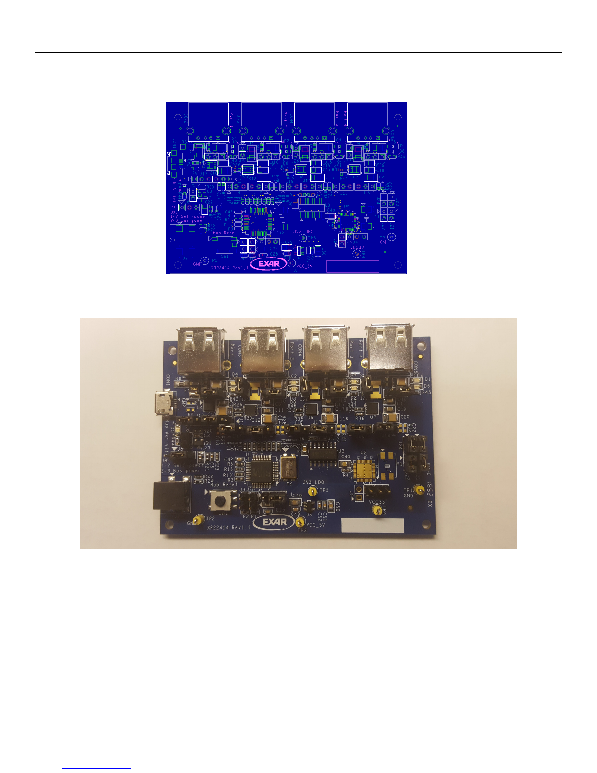
Evaluation Board outline
Figure 1 shows the topography of the evaluation board. Either U1 or U2 will be installed depending upon the version of the
evaluation board.
Figure 1: XR22414 PCB Outline
Table 1: Ordering Information
Device Ordering Part Number Evaluation Board Ordering Part Number Device Package Device Location
XR22414CV48-F XR22414CV48EVB LQFP 48 U1
XR22414CL48-F XR22414CL48EVB QFN 48 U2
U
S
B
QFN
48
PWR
DS Port
1
DS Port
2
DS Port
3
DS Port
4
U2
P
T
CJUMP
C
M
LED
CAP
JUMP
LED
J8
J8: 1-2 Self Power
2-3 Bus Power
LQFP
48
1
24
48
12
U1
LED
P
T
CJUMP
C
M
LED
CAP
LED
P
T
CJUMP
C
M
LED
CAP
LED
P
T
CJUMP
C
M
LED
CAP
LED
© 2017 Exar Corporation
XR22414 EVB User’s Manual
2 / 8 www.exar.com\XR22414
Rev 1A
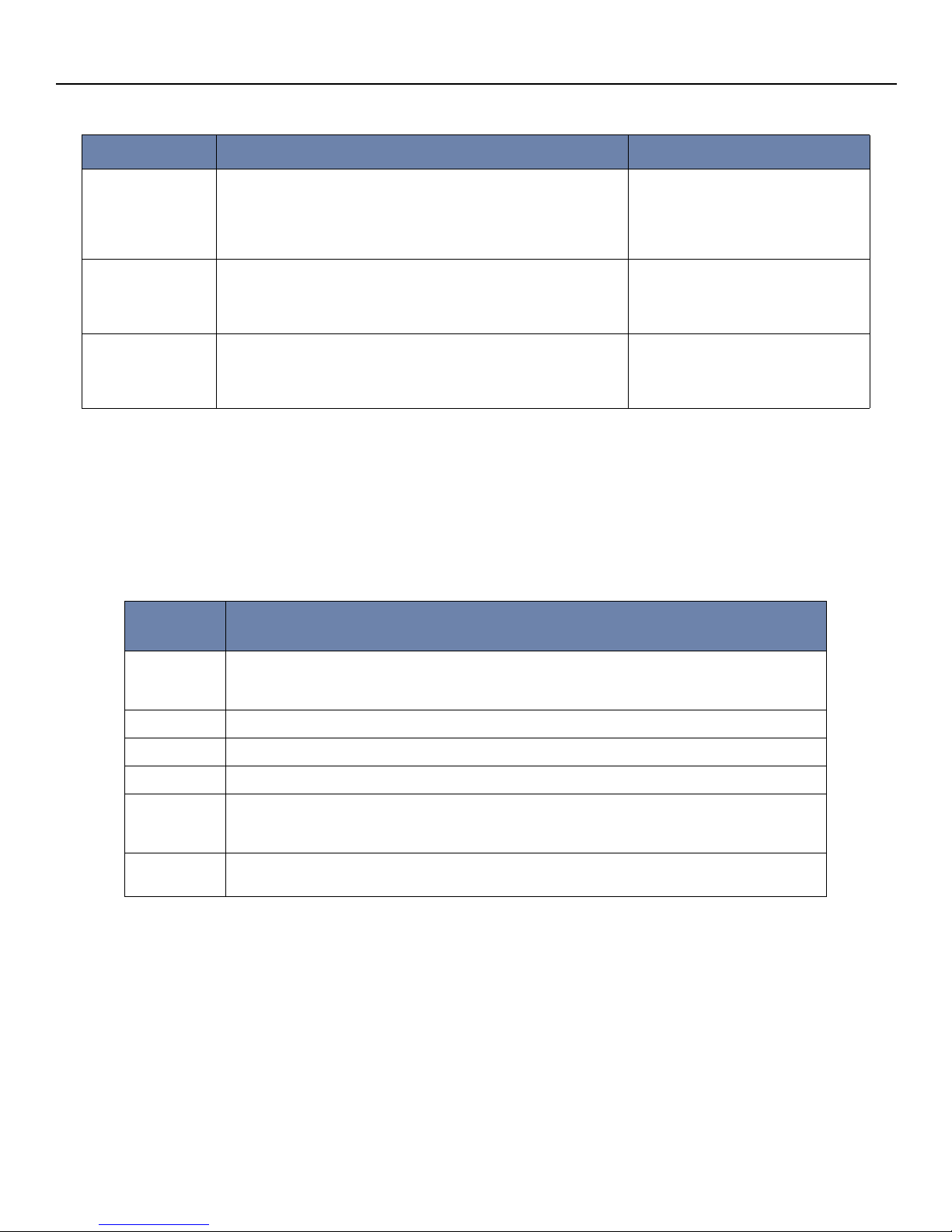
Evaluation Board Layout
Evaluation Board Picture
Figure 2: XR22414 PCB
Hardware Configuration
This section describes the default board settings, when shipped from the factory, and jumper settings that may be used to
reconfigure operation.
Differences between XR22414CV48EVB and XR22414CL48EVB
The XR22414 is available in two packages, a 48 pin LQFP and a 48 pin QFN. The two versions of the evaluation board use
the same bare PCB, but with different components assembled, which includes either the LQFP or QFN package. In order to
avoid trace stubs on high speed USB (480 MHz) nets, 0 ohm resistors are installed from the upstream and all four down-

© 2017 Exar Corporation
XR22414 EVB User’s Manual
3 / 8 www.exar.com\XR22414
Rev 1A
stream USB ports to connect to the QFN48 device for the XR22414CL48EVB. These resistors are not installed for the
LQFP48 EVB.
Power Configurations
The XR22414 EVB may operate in either bus powered or self-powered modes. The power mode must be selected by
jumper J8. If self-powered, the device uses the 5V supplied by the external 5V DC input to J8 power jack. When bus pow-
ered, the XR22414 may not be capable of providing sufficient power to all downstream ports. By USB specification, in bus
powered mode, each downstream port may draw 100 mA maximum and the hub itself may draw an additional 100 mA. In
self-powered mode, external 5V must be supplied to the PCB via the J7 power connector and each downstream port may
draw up to 500 mA.
The XR22414 EVB may alternately operate from a 3.3V input. To power the device from 3.3V the REG_EN# pin must be
deasserted and the VCC5 pin must not be connected to a 5V source. The 3.3V power input to should be provided to all
VCC33 pins and the 3V3_OUT pin will not provide an output voltage.
The XR22414 EVB can be configured for either individual or global power monitoring and ganged power control. In individ-
ual mode, each port is monitored by an XRP2527 power monitor circuit. In global mode, all four downstream ports power is
combined and monitored by a single monitor circuit. Alternately, power to the downstream ports of the XR22414 EVB can
be monitored by a resettable PTC fuse, or by both the fuse and the power monitor devices. Over-current conditions detected
by either XRP2527 current monitors or PTC fuses are signaled to the OVC# pin of the device, and power out pins (PWR#)
are deasserted to then power down downstream ports.
Table 2 defines the jumper settings on the XR22414 EVB, and the default settings of each jumper when shipped from the
factory.
Table 2: Jumper Settings and components for PCB Power
Jumper Description Default
J8 J8 must be installed either pin 1 to 2 when the XR22414 is self-powered
or pin 2 to 3 when the device is bus powered.
By default J8 is installed pin 1 to 2
J6 J6 can be used to bypass the inrush current limiting circuit when the
XR22414 is bus powered.
By default J6 is not installed
J1, J2, J3, J4, J5 To power the device from 3.3V instead of 5V, the top surface trace
across jumper J3 must be cut disabling the 5V to 3.3V internal regulator.
For the XR22414CV48EVB the top surface trace across jumper J2 must
also be cut and J1 must be installed from pin 2 to 3 to use the external
3.3V LDO voltage. For the XR22414CL48EVB J5 trace must be cut and
J4 must be installed pin 2 to 3.
J2, J3 and J5 are normally not installed.
By Default, J1 in installed pin 1 to 2 for
the XR22414CV48EVB or J4 is installed
pin 1 to 2 for the XR22414CL48EVB.
J21, J22, J23, J24,
J25, J26, J27
J21 is used to select global over current monitoring for downstream port
over-current protection. When J21 is installed, global over-current moni-
toring is selected. When J21 is not installed, individual port over-current
monitoring is selected. If J21 is installed, J25, J26 and J27 should also
be installed to connect port power for all downstream ports together and
J22, J23, and J24 should also be installed to connect unused OVCn#
pins to ground.
By default J21, J22, J23, J24, J25, J26
and J27 are not installed.
J9, J10, J15, J16 J9, J10, J15 and J16 are used to select whether the PTC fuse only or
current monitor (XRP2527) device is used for downstream port over-cur-
rent protection.
By default J9, J10, J15 and J16 are
installed from pin 1 to 2.
J11, J12, J17, J18 If J9, J10, J15 and J16 are installed pin 1 to 2, J11, J12, J17 and J18
select whether XRP2527 over-current monitor only or PTC fuse and cur-
rent monitor devices protect downstream ports.
By default J11, J12, J17 and J18 are
installed from pin 2 to 3.
© 2017 Exar Corporation
XR22414 EVB User’s Manual
4 / 8 www.exar.com\XR22414
Rev 1A
Uninstalled components on XR22414CV48EVB and XR22414CL48EVB
Both XR22414 EVBs have a number of components that are not installed. These components have a variety of purposes
and some may be installed after cutting the surface “shorting traces” which short across the pins of the devices when they
are not installed.
LED Indicators
Each USB port of the XR22414 EVBs has green and amber activity indicators. The upstream port has a single blue LED to
indicate any hub activity. The hub activity LED is lit when the hub is connected to a USB host. However, if there are no
downstream ports connected, following device enumeration and a short period of inactivity, the hub will be placed in sus-
pend state and the hub activity LED will not be lit. The 4 downstream ports have green LEDs for port activity and amber
indicators for error indications including over-current per USB 2.0 specifications chapter 11.
J13, J14, J19, J20 When J13, J14, J19 and J20 are installed from pin 2 to 3, the XRP2527
current monitors use USB 2.0 default trip voltage. If installed pin 1 to 2,
the current monitors trip at the value established by the resistance of the
RSET pin to ground using formula ILIM (trip current) = ~108.7 / RSET
resistance (kOhms).
By default, J13, J14, J19 and J20 are
installed pin 1 to 2.
J9 J9 selects normal hub operation port and hub activity indicators or
charging mode.
By default J9 is installed pin 2 to 3 for
normal hub operation and LED activity
indicators. Must be installed pin 1 to 2 to
enable charging mode.
F2, F3, F4 F1, F2, F3 and F4 may be used instead of, or in conjunction with the
XRP2527 current monitors. Only F1 is populated by default on the
XR22414 EVB with the intent that F1 may be used in global over-current
protection modes.
Only F1 is populated by default
Table 3: Uninstalled Components
Uninstalled
Components
J2 & J5 By default J2 and J5 are not installed. For power measurements, an ammeter may be installed by cutting
either the surface trace on J2 (when using the LQFP48 device) or J5 (when using the QFN48 device). J1 or
J2 can then be installed or an ammeter in series can be used for power measurements.
J3, J6 By default J3 and J6 not installed.
CM1 - CM5 Common Mode chokes on upstream and 4 downstream ports for EMI purposes.
R10- R19 R10- R19 are not installed on XR22414CV48EVB to prevent stubs on high speed USB traces.
C13. C14,
C21, C22, R27,
R28, R33, R34
C13. C14, C21, C22, R27, R28, R33, and R34 are not installed.
Y1 / Y2 and
R4 / R5
For the XR22414CV48EVB Y1 and R4 are not installed. For the XR22414CL48EVB Y2 and R5 are not
installed.
Table 2: Jumper Settings and components for PCB Power
Jumper Description Default

© 2017 Exar Corporation
XR22414 EVB User’s Manual
5 / 8 www.exar.com\XR22414
Rev 1A
XR22414 Evaluation Board Bill of Materials
The Bill of Materials for the two versions of the XR22414 evaluation boards are in the following tables. The
XR22414CV48EVB BOM is in Table 4 and XR22414CL48EVB in Table 5. Several component part numbers marked “DNI”
may typically be not installed on the Exar evaluation boards. However, these may be used on customer PCBs for EMI or
other purposes as desired.
Table 4: XR22414CV48EVB BOM (Rev. 1.1 PCB)
Item Qty Ref. Des Description Part Number
1 5 CM1, CM2, CM3, CM4, CM5 Common Mode Choke Surface Mount 744230900_DNI
2 4 CON2, CON3, CON4, CON5 USB Conn, Receptable, A-type 61400416021
3 1 CON1 Connector, USB_MICRO_ B 629105150521
4 8 C1, C2, C4, C6, C10, C12, C18, C20 Ceramic Capacitor, 47uF/16V 1210 885012109011
5 2 C26, C27 Ceramic Capacitor, 4.7uF/16V 0805 885012107013
6 2 C28, C40 Ceramic Capacitor, 10uF/16V 0805 885012107014
7 10 C7, C8, C9, C11, C15, C16, C17, C19, C49, C50 Ceramic Capacitor, 1uF/16V, 0805 885012207051
8 16 C3, C5, C23, C25, C31, C35, C36, C37, C38, C42,
C43, C44, C45, C48, C51, C52
Ceramic Capacitor, 100nF/25V 0603 885012206071
9 4 D2, D3, D4, D5 LED, Green, 0805 150080GS75000
10 1 D5 LED, Blue, 0805 150080BS75000
11 4 D6, D7, D8, D9 LED, Amber, 0805 150080YS75000
12 1 F1 PTC Resettable, 0.75A 8V 1812 MF-MSMF075-2
13 3 F2, F3, F4 PTC Resettable, 0.75A 8V 1812 DNI MF-MSMF075-2_DNI
14 14 J1, J8, J9, J10, J11, J12, J13, J14, J15, J16, J17,
J18, J19, J20
3 Positions Header, 0.100" (2.54mm) 61300311121
15 1 J4 3 Positions Header, 0.100" (2.54mm) DNI 61300311121_DNI
16 7 J21, J22, J23, J24, J25, J26, J27 2 Positions Header, 0.100" (2.54mm) 61300211121
17 4 J2, J3, J5, J6 2 Positions Header, 0.100" (2.54mm) 61300211121_DNI
18 1 J7 Connector, Power Jack, DC RA SMD 694103107102
19 1 Q1 MOSFET P-CH 12V 4.1A SOT-23 SI2333DS-T1-E3
20 1 R5 Resistor, 2.7 kOhm, 1%, 0603
21 1 R8 Resistor, 0 Ohm, 0603
22 11 R9, R10, R11, R12, R13, R14, R15, R16, R17, R18,
R19
Resistor, 0 Ohm, 0603 DNI DNI
23 4 R29, R30, R35, R36 Resistor, 215 kOhm, 5%, 0603
24 10 R2, R3, R6, R7, R21, R24, R25, R26, R31, R32 Resistor, 10 kOhm, 5%, 0603
24 1 R23 Resistor, 100 kOhm, 5%, 0603
25 1 R28, R28,R33, R34 Resistor, 100 kOhm, 5%, 0603 DNI
26 2 R1,R22 Resistor, 5.1 kOhm, 5%, 0603

© 2017 Exar Corporation
XR22414 EVB User’s Manual
6 / 8 www.exar.com\XR22414
Rev 1A
Note: Part numbers marked _DNI are not installed.
27 1 R44 Resistor, 470 Ohm, 5%, 0603
28 4 R43, R45, R46, R47 Resistor, 2 kOhm, 5%, 0603
29 1 R20 Resistor, 40.2 KOhm, 1%, 0603
30 1 SW1 Switch, SPST-NO 431481031816
31 5 TP1, TP2, TP3, TP4, TP5 Test Point PC Mini .040"D Yellow 36-5004-ND
32 1 U1 IC, USB 2.0 Hub, 4 Port, LQFP48 XR22414CV48-F
33 4 U4, U5, U6, U7 USB Current Monitor, DFN8 2x3 XRP2527IHB-1-F
34 1 U8 LDO 5V to 3.3V SP6260GEK-L/TR_DNI
35 1 U3 Hex Inverter IC SN74LVC14ADRG3
36 1 Y2 12MHz ±20ppm Crystal 18pF -20°C ~ 70°C
4-SMD
ABMM-12.000MHZ-B2-T
Table 5: XR22414CL48EVB BOM (Rev. 1.1 PCB)
Item Qty Ref. Des Description Part Number
1 5 CM1, CM2, CM3, CM4, CM5 Common Mode Choke Surface Mount 744230900_DNI
2 4 CON2, CON3, CON4, CON5 USB Conn, Receptable, A-type 61400416021
3 1 CON1 Connector, USB_MICRO_ B 629105150521
4 8 C1, C2, C4, C6, C10, C12, C18, C20 Ceramic Capacitor, 47uF/16V 1210 885012109011
5 2 C26, C27 Ceramic Capacitor, 4.7uF/16V 0805 885012107013
6 2 C28, C40 Ceramic Capacitor, 10uF/16V 0805 885012107014
7 10 C7, C8, C9, C11, C15, C16, C17, C19, C49, C50 Ceramic Capacitor, 1uF/16V, 0805 885012207051
8 15 C3, C5, C24, C25, C30, C32, C33, C34, C39, C42,
C46, C47, C48, C51, C52
Ceramic Capacitor, 100nF/25V 0603 885012206071
9 4 D2, D3, D4, D5 LED, Green, 0805 150080GS75000
10 1 D5 LED, Blue, 0805 150080BS75000
11 4 D6, D7, D8, D9 LED, Amber, 0805 150080YS75000
12 1 F1 PTC Resettable, 0.75A 8V 1812 MF-MSMF075-2
13 3 F2, F3, F4 PTC Resettable, 0.75A 8V 1812 DNI MF-MSMF075-2_DNI
14 14 J4, J8, J9, J10, J11, J12, J13, J14, J15, J16, J17,
J18, J19, J20
3 Positions Header, 0.100" (2.54mm) 61300311121
15 1 J1 3 Positions Header, 0.100" (2.54mm) DNI 61300311121_DNI
16 7 J21, J22, J23, J24, J25, J26, J27 2 Positions Header, 0.100" (2.54mm) 61300211121
17 4 J2, J3, J5, J6 2 Positions Header, 0.100" (2.54mm) 61300211121_DNI
18 1 J7 Connector, Power Jack, DC RA SMD 694103107102
Table 4: XR22414CV48EVB BOM (Rev. 1.1 PCB)
Item Qty Ref. Des Description Part Number

© 2017 Exar Corporation
XR22414 EVB User’s Manual
7 / 8 www.exar.com\XR22414
Rev 1A
Note: Part numbers marked _DNI are not installed.
19 1 Q1 MOSFET P-CH 12V 4.1A SOT-23 SI2333DS-T1-E3
20 1 R4 Resistor, 2.7 kOhm, 1%, 0603
21 12 R8, R10, R11, R12, R13, R14, R15, R16, R17, R18,
R19
Resistor, 0 Ohm, 0603
22 1 R9 Resistor, 0 Ohm, 0603 DNI DNI
23 4 R29, R30, R35, R36 Resistor, 215 kOhm, 5%, 0603
24 10 R2, R3, R6, R7, R21, R24, R25, R26, R31, R32 Resistor, 10 kOhm, 5%, 0603
24 1 R23 Resistor, 100 kOhm, 5%, 0603
25 1 R28, R28,R33, R34 Resistor, 100 kOhm, 5%, 0603 DNI
26 2 R1,R22 Resistor, 5.1 kOhm, 5%, 0603
27 1 R44 Resistor, 470 Ohm, 5%, 0603
28 4 R43, R45, R46, R47 Resistor, 2 kOhm, 5%, 0603
29 1 R20 Resistor, 40.2 KOhm, 1%, 0603
30 1 SW1 Switch, SPST-NO 431481031816
31 5 TP1, TP2, TP3, TP4, TP5 Test Point PC Mini .040"D Yellow 36-5004-ND
32 1 U2 IC, USB 2.0 Hub, 4 Port, QFN48 XR22414CL48-F
33 4 U4, U5, U6, U7 USB Current Monitor, DFN8 2x3 XRP2527IHB-1-F
34 1 U8 LDO 5V to 3.3V SP6260GEK-L/TR_DNI
35 1 U3 Hex Inverter IC SN74LVC14ADRG3
36 1 Y1 12MHz ±20ppm Crystal 18pF -20°C ~ 70°C
4-SMD
ABMM-12.000MHZ-B2-T
Table 5: XR22414CL48EVB BOM (Rev. 1.1 PCB)
Item Qty Ref. Des Description Part Number
© 2017 Exar Corporation
XR22414 EVB User’s Manual
8 / 8 www.exar.com\XR22414
Rev 1A
For Further Assistance:
Email: UARTtechsupport@exar.com
Exar Technical Documentation: http://www.exar.com/techdoc/
Exar Corporation Headquarters and Sales Offices
48720 Kato Road Tel: +1 (510) 668-7000
Fremont, CA 95438 - USA Fax: +1 (510) 668-7001
NOTICE
EXAR Corporation reserves the right to make changes to the products contained in this publication in order to improve design, performance or reliability. EXAR Corporation
assumes no responsibility for the use of any circuits described herein, conveys no license under any patent or other right, and makes no representation that the circuits are free
of patent infringement. Charts and schedules contained herein are only for illustration purposes and may vary depending upon a user’s specific application. While the information
in this publication has been carefully checked; no responsibility, however, is assumed for inaccuracies.
EXAR Corporation does not recommend the use of any of its products in life support applications where the failure or malfunction of the product can reasonably be expected to
cause failure of the life support system or to significantly affect its safety or effectiveness. Products are not authorized for use in such applications unless EXAR Corporation
receives, in writing, assurances to its satisfaction that: (a) the risk of injury or damage has been minimized; (b) the user assumes all such risks; (c) potential liability of EXAR Cor-
poration is adequately protected under the circumstances.
Reproduction, in part or whole, without the prior written consent of EXAR Corporation is prohibited.
Revision History
Revision Date Description
1A February 2017 Initial release
Table of contents
Other Exar Motherboard manuals

Exar
Exar XR21B1424IV64-0A-EVB User manual

Exar
Exar XRA1403IL24-F User manual

Exar
Exar XRP6142 User manual

Exar
Exar XR20M1280 User manual

Exar
Exar Power XR Series User manual

Exar
Exar XRP7740EVB-HIC Operating and maintenance instructions

Exar
Exar SP338 User manual

Exar
Exar XRP6141 User manual

Exar
Exar XRP7664-65-74-75 User manual

Exar
Exar SP336E User manual


