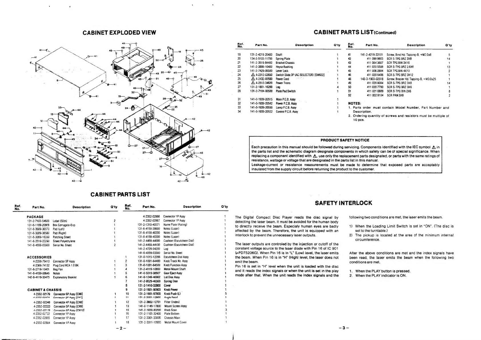
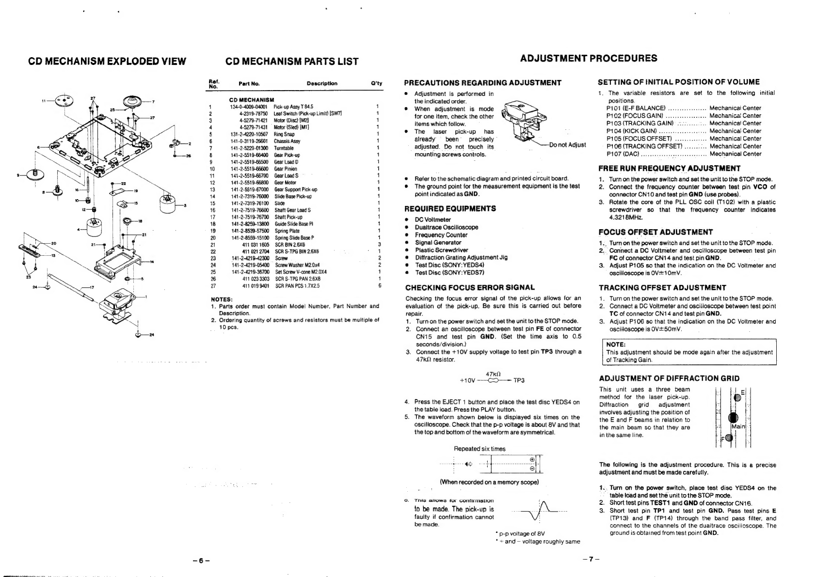
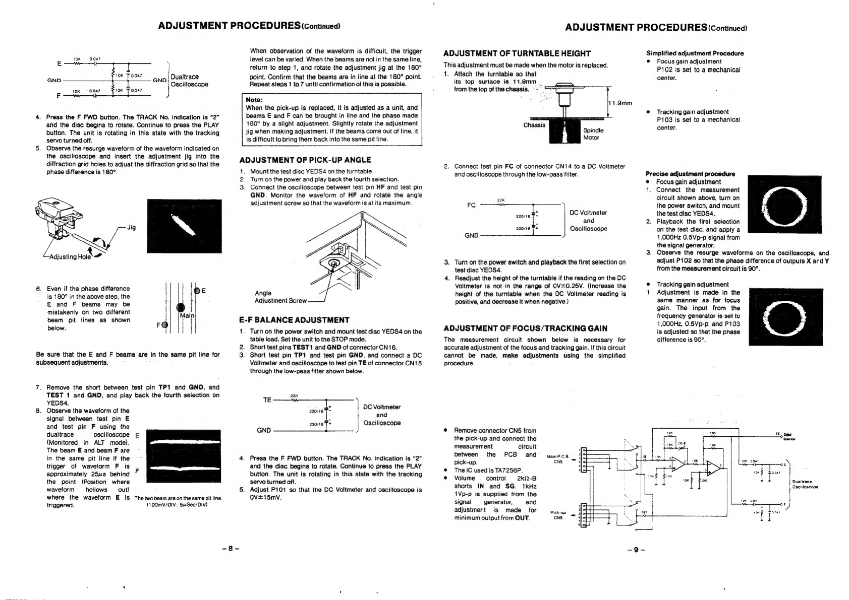
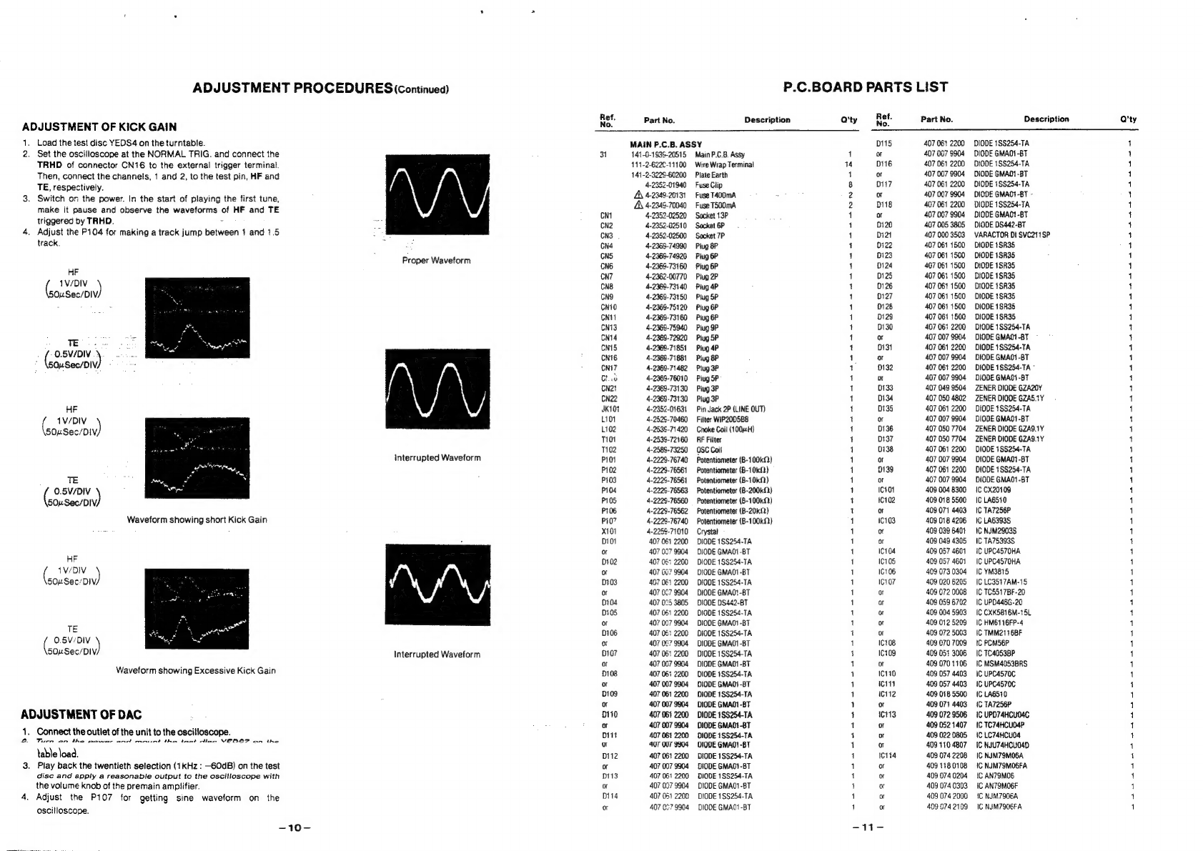
Fisher DAC-204 User manual

SERVICE
MANUAL
DIGITAL
COMPACT
DISC
PLAYER
4r|
FISHER
DAC-204
(EUROPE)
137
326
42
SPECIFICATIONS
System
.................
Compact
disc
digital
audio
system
Program
Functions
.................0:c:eeeeeee
32
selections
Program
Reset
..................0ce000s
Press
CLEAR
button
AUDIO
CHARACTERISTICS
Checking
Program
......cccccccceeseee:
With
CHECK
button
Frequency
Response
.............-..600.00s
20
Hz
—
20
kHz
(in
STOP
mode)
:
. .
Lo}
Harmonic
Distortion
............
Less
than
0.006
%
(1
kHz)
Intro
SCAN
ooo...
ee
cceeceeceeee
sees
1
~
99
sec.
programable
S/N:
Rath
ei
iic.
cerrado
ce ge
eed
More
than
90
dB
ms
:
'S
ea
aes
:
Wow
and
Flutter
Helaw
deceurabie
itnis
Scanning
........
2
speed
fast-forward/back
with
sound,
Ch
is
gS
a
EE
eee
M
than
80
dB
(1
kHz)
2
speed
search
in
PAUSE
mode
annel
Separation
.............5
Crenthan
7
Random
Disc
Play
..........
Press
RANDOM
PLAY
button
FUNCTIONS
Total
Disc
Time
Display
....
Press
DISPLAY
button
twice
Disc
Selection
..............ccceceee
eee
With
DISC
NUMBER
Repeat
................685
All
tracks,
all
programmed
tracks
.
(1
~
5)
buttons
.
a
veel
.
GENERAL
Track
Selection
................00eeeee
With
TRACK/INDEX
Power
Requirements
(50
Hz)
.........6..6...
AC
110/220V
NUMBER
(0
~
9)
buttons
20
Waits
INDE
Aeo
RISC
UMN
saan
ear
ey
Dimensions
(WxHxD)
.......c0
440
x
113x290
mm
Wei
sangeet
2
Som
ns
Besattan
bald
at
ene
Nt
ect
atedhal
:
(normal
disc
play
only)
eight
lapproxs
SRG
Program
Selection
..........
With
DISC
NUMBER
(1
~
5),
sepninia
ten
eee
ee
SS
9)
1S
REFERENCE
No.
WM-19866

CABINET
EXPLODED
VIEW
CABINET
PARTS
LIST
Ret
Part
No.
Description
Q'ty
Ret.
Part
No.
PACKAGE
4-2352-02866
131-2-7103-54600
—
Label
(50th)
131-6-1169-2089
Box
Corrugate-Exp.
131-6-3009-36570
Pad
(Left)
131
-6-3009-36580
Pad
(Right)
131-6-3069-16350
Patching
Sheet
141-6-2519-22230
Sheet
Polyethylene
141-6-4559-03300
Seriai
No.
Sheet
ACCESSORIES
4-2359-79410
Connector
5P
Assy
4-2369-74132
Plug
Cord
RCA
1.0
BK
131-6-2719-10401
Bag
Fan
141-6-4159-00645
Notes
142-6-4119-33475
Explanatory
Booklet
CABINET
&
CHASSIS
4-2352-02179
Connector
6P
Assy
[CN6}
4-2952-02474
—
Connegtor
@P
Agay
(CN7]
4-2352-02348
Connector
4P
Assy
[CN8)
4-2352-02333
Connector
5P
Assy
ICN9]
4-2352-02178
—
Connector
6P
Assy
[CN10]
4-2352-02722
Connector
1P
Assy
4-2352-02865
Connector
1P
Assy
4-2352-02854
Connector
iP
Assy
lath
man
ae
ay
et
Nock:
Sek
ts
Se
OOIAMAHARWN
4-2352-02867
131-2-1310-40571
131
-6-4159-39600
131-6-4159-40200
131-6-4159-40300
141-2-4459-44000
141-2-4459-441
00
141-2-4729-04200
141-6-4559-03300
131-0-1015-12206
131-0-1001-64400
131-0-1001-64500
131-2-4119-10800
141-0-5519-08507
141-0-1249-46902
141-2-8529-40300
131-2-1440-32800
131-2-1601
-90903
131
-2-1601-97800
131-2-3201
-12800
131-2-3602-12701
141-0-1149-17800
141-2.1659-83200
134
-2-1105-32400
431-2-3301-33006
431-2-3314-10900
Description
Connector
1P
Assy
Connector
1P
Assy
Name
Plate
(Rating)
Notes
(Laser)
Notes
(Laser)
Notes
(Laser)
Cushion
(Escutcheon
Dial)
Cushion
(Escutcheon
Dial)
Lug
Serial
No.
Sheet
Escutcheon
Dial
Assy
Knob
Track
No.
Assy
Knob
Function
Assy
Metal
Mount
Shaft
Gear
Eject
Assy
Lid
Disc
Assy
Spring
Door
Cover
Knob
Power
Knob
Push
{L)
Angie
Reinf
Filter
(Index)
Mount
Screen
Assy
Knob
Scan
Plate
Bottom
Chassis
Main
Metal
Mount
Cover
Q'ty
oe
ewe
eee
CABINET
PARTS
LIST
continued)
Ret
Part
No.
No.
Description
arty
19
131-2-4219-20400
Shaft
1
20
134-2-5103-11700
Spring
Plate
1
2
141-2-3518-84400
Bracket
Chassis
1
22
141-2-3899-10400
Heyco
Bushing
1
23
141-2-7429-06500
Lever
Lock
1
24
AX
4-2312-02650
Switch
Slide
3P
(AC
SELECTOR)
[Sw602]
1
25
AM
4-2432-00500
Power
Cord
}
1
26
A\
4-2512-34620
Power
Trans 1
27
131-2-1801-16200
Leg
4
28
131-2-7104-00500
Plate
Pad
Switch
1
141-0-1939-20515
Main
P.C.B.
Assy
141-0-1939-20542
Power
P.C.B.
Assy
141-0-1939-20550
Lamp
P.C.B.
Assy
141-0-1939-20522
Control
P.C.B.
Assy
RBRS
ner
Part
No.
Description
Q’ty
4i
141-2-4219-33101
Screw,
Bind
Hd.
Tapping-B,
+M3.0x8
§
42
411
099.9803
SCR
S-TP6
BRZ
3x8
14
4
411064
3607
SCR
TPG
BIN
3X16
1
44
4110205508
SCR
S-TPG
BRZ
2.6X6
13
45
411
006
2804
SCR
TPG
BIN
4X10
2
46
411
0206406
SCR
S-TPG
BRZ
3xt2
1
48
143-3-1903-02518
Screw,
Brazier
Hd.
Tapping-B,
+M3.0x25
1
49
411
020
8004
SCR
S-TPG
BRZ
3x8
14
50
4110207700
SCR
S-TPG
BRZ
3x6
1
51
411.021.0808
SCR
S-TPG
BIN
2X6
8
52
4110029104
SCR
PAN
3X8
2
NOTES:
1.
Parts
order
must
contain
Model
Number,
Part
Number
and
Description.
2.
Ordering
quantity
of
screws
and
resistors
must
be
multiple
of
10
pcs.
PRODUCT
SAFETY
NOTICE
Each
precaution
in
this
manua!
should
be
followed
during
servicing.
Components
identified
with
the
EC
symbol
A\
in
the
parts
list
and
the
schematic
diagram
designate
components
in
which
safety
can
be
of
special
significance.
When
replacing
a
component
identified
with
A\,
use
only
the
replacement
parts
designated,
or
parts
with
the
same
ratings
of
resistance,
wattage
or
voltage
that are
designated
in
the
parts
list
in
this
manual.
Leakage-current
or
resistance
measurements
must
be
made
to
determine
that
exposed
parts
are
acceptably
insulated
from
the
supply
circuit
before
returning
the
product
to
the
customer.
SAFETY
INTERLOCK
The
Digital
Compact
Disc
Player
reads
the
disc
signal
by
detecting
the
taser
beam.
It
must
be
avoided
for
the
human
body
to
directly
receive
the
beam.
Especialy
human
eyes
are
badly
affected
by
the
beam.
Therefore,
the
unit
is
equipped
with
an
interlock
to
prevent
the
unnecessary
laser
outputs.
The
laser
outputs
are
controled
by
the
injection
or
cutoff
of
the
constant
voltage
source
to
the
laser
diode
with
Pin
16
of
IC
901
(«PD75206G).
When
Pin
16
is
in
“L”
(Low)
level,
the
laser
emits
the
beam.
When
Pin
16
is
in
“H”
(High)
level,
the
laser
does
not
emit
the
beam.
Pin
16
is
set
in
“H”
level
when
the
unit
is
loaded
with
the
disc
and
it
reads
the
index
signals
or
when
the
unit
is
set
in
the
play
mode
after
that.
When
the
unit
reads
the
index
signals
and
the
following
two
conditions
are
met,
the
laser
emits
the
beam.
1)
When
the
Loading
Limit
Switch
is
set
in
“ON”.
(The
disc
is
set
to
the
turntable.)
2)
The
pickup
is
located
at
the
area
of
the
minimum
internal
circumference.
After
the
above
conditions
are
met
and
the
index
signals
have
been
read,
the
laser
emits
the
beam
when
the
following
two
conditions
are
met.
1.
When
the
PLAY
button
is
pressed.
2.
When
the
PLAY
indicator
is
ON.

CD
INDEX
MECHANISM
EXPLODED
VIEW
CD
INDEX
PARTS
LIST
icontinueg)
Ref.
Part
No.
Description
Q'ty
Ret:
Part
No.
Description
Q'ty
44
141-2-8539-61300
Spring
Lever
Rock
1
67
4110207007
SCR
S-TPG
BRZ
3x20
2
45
141-2-8539-61400
Spring
Plate
1
68
411
0205904
SCR
S-TPG
BAZ
3X10
13
46
141-2-8549-39200
Spring
Lever
index
1
69
4110207700
SCR
S-TPG
BRZ
3X6
4
47
141-2-7319-89600
Slide Plate
Left
1
70
4110205508
“SCR
S-TPG
BRZ
2.6x6
5
48
141-2-8549-41900
Spring
Siide
Plate
Left
1
ral
4110221904
SCR
S-TPG
FLT
2.6X6
1
72
4110310103
SCR
BIN
2.6X3
2
51
141-0-1939-19830
LED
P.C.B.
Assy
1
73
4110310905
SCR
BIN
2.6x4
2
52
141-0-1939-19840
Photo
Transistor
P.C.B.
Assy
1
74
4110307707
SCR
BIN
2x8
2
53
141-0-1939-19850
Photo
Sensor
P.C.B.
Assy
1
75
4110637309
SCR
TPG
BIN
2X10
3
76
411
063
8504
SCR
TPG
BIN
2x8
1
61
141-2-4219-04200
Screw
5
62
141-2-4219-05400
Screw
Washer
2
NOTES:
63
131-2-4201-28201
Screw(b
Tite
Sems)
1
1.
Parts
order
must
contain
Model
Number,
Part
Number
and
64
131-2-4201-28300
Screw(b
Tite
Sems)
Z
2
Description.
65
141-2-4219-44800
+BRTS-B
M2.6X14
Sems
4
2.
Ordering
quantity
of
screws
and
resistors
must
be
multiple
of
66
141-2-4219-23000
Screw
1
10
pes.
SAFETY
CERTIFICATION
This
Compact
Disc
Player
is
made
and
tested
to
meet
exacting
safety
standards.
It
meets
UL
and
FCC
requirements
and
complies
with
safety
performance
standards
of
the
U.S.
Department
of
Health
and
Human
Services.
CD
INDEX
MECHANISM
PARTS
LIST
Ret:
Part
No.
Description
a’ty
Ret.
Part
No.
Description
Q'ty
CD
INDEX
MECHANISM
;
19
141-2-5519-73700
Gear
Pinion
2
meses
Berea
oe
Se
141-2-2449-55200
Sheet
1
20
141-2-5619-02800
Belt
(Timing)
1
141-2-4729-04200
Lug
1
21
141-2-5649-30300
Belt
2
141-2-4729-07100
Wire
Band
7
22
141-2-6229-01600
Support
Front
1
1
141-2-4579-05900
Washer,
M4.7x9.0x0.13
2
23
141-2-6229-01700
Support
Rear
1
2
4-2319-79910
Lever
Switch
(Open/Close)
[SW1]
1
24
141-2-6229-01800
Flap
Disc
Cramp
‘
-
i
int)
(SW2
1
Ye
141-2-7319-85800
Tray
;
ene
rena
renee
cece
(swa
1
26
141-2-7319-85900
Slide
Lett
1
CAUTION
—
USE
OF
CONTROLS
OR
ADJUSTMENTS
OR
PERFORMANCE
OF
PROCEDURES
OTHER
THAN
2
4-2319-79910
Lever
Switch
(Playback
Point)
[SW4]
1
27
141-2-7319-86000
Sjide
Right
1
THOSE
SPECIFIED
HEREIN
MAY
RESULT
IN
HAZARDOUS
RADIATION
EXPOSURE.
3
4-5279-71630
Motor
(index)
[M3]
1
28
|
141-2-7429-05800
Lever
Cam
Left
1
4
4-5279-71631
Motor
Load
(Load)
[M4]
1
29
141-2-7429-05900
Lever
Eject
1
THE
COMPACT
DISC
PLAYER
SHOULD
NOT
BE
ADJUSTED
OR
REPAIRED
BY
ANYONE
EXCEPT
QUALIFIED
5
141-0-7319-36100
Slide
Plate
Assy
1
30
141-2-7429-06000
Lever
Stop
1
SERVICE
PERSONNEL.
8
141-0-7419-44200
Lever
index
Assy
1
3h.
~~
141-2-7429-06100
prop
:
en
ed
eee
7
141-0-7439-20900
Arm
index
Assy
1
32
141-2-7429-06200
Lever
Adjust
8
141-0-8619-00300
Magnet
Assy
1
33;
-:
--141-2-7519-83000
Shaft
Gear
Worm
1
LASER
BEAM
RADIATION
SPOT
9
141-2-4459-42000
Cushion
Rubber
4
4
141-2-7519-83100
Shaft
Index
1
10
141-2-3119-30200
Chassis
(Load)
1
35
141-2-7519-83200
Pin
Adjust
1
Laser
Beam
Radiation
1
141-2-3519-83800
Holder
Disc
1
36
141-2-7519-83300
Shaft
Lever
Rock
1
12
141-2-5519-73000
Gear
Wormwheel
1
KYA
141-2-8219-37500
Guide
Left
1
43
141-2-5519-73100
Gear
Index
1
3B
141-2-8219-37600
Guide
Right
1
14
141-2-5519-73200
Gear
Worm
1
39
4141-2-8219-37700
Guide
Plate
1
15
141-2-5519-73300
Gear
Cam
Left
1
40
141-2-8459-04900
Cap
Gear
Pinion
2
+2
+44
2
BEIM.
20400
Baar
Qam
Right
1
a
141-2.8529-39500
Sorina
Lever
Stop
2
WO
ACETCT
Gear
Putey
1
&@_——*141-2-8929-39600
Spring
Arm
index
1
Laser
Dioda
Properties
18
141-2-$519-73600
Gear
Load
1
43
141-2-8529-39700
Spring
Lever
Adjust
1
Material
:
Ga-Al-As
Wavelength
:
755
—
815 nm
(25°C)
Laser
Output
:
Continuous
Wave
max.
0.5
mW
7

CD
MECHANISM
EXPLODED
VIEW
CD
MECHANISM
PARTS
LIST
ADJUSTMENT
PROCEDURES
Ret.
Part
No.
Description
arty
PRECAUTIONS
REGARDING
ADJUSTMENT
SETTING
OF
INITIAL
POSITION
OF
VOLUME
@
Adjustment
is
performed
in
1.
The
variable
resistors
are
set
to
the
following
initial
CD
MECHANISM
the
indicated
order.
positions.
1
134-0-4009-04001
Pick-up
Assy
T
84.5
a)
1
@
When
adjustment
is
mode
P4101
(E-F
BALANCE)
...............-.
Mechanicai
Center
2
4-2319-78750
Leaf
Switch
(Pick-up
Limit)
[SW7]
:
for
one
item,
check
the
other
P102
(FOCUS
GAIN)
.....
....
Mechanica!
Center
4
45279-71421
Motor
(Diec)
(M2)
:
items
which
follow.
P103
(TRACKING
GAIN)
”...
Mechanicat
Center
4
4-5279-71431
Motor
(Sled)
[M1]
1
:
ical
5
131-2-4220-10507
Ring
Snap
{
@
The
iaser
pick-up
has
P104
(KICK
GAIN)
........
—
Mechanical
Center
6
141-0-3119-26601
Chassis
Assy
1
already
been’
precisely
P105
(FOCUS
OFFSET)
Mechanical
Center
7
141-2-5229-01300
Turntable
1
adjusted.
Do
not
touch
its
;
P106
(TRACKING
OFFSET)
.......:..
Mechanical
Center
8
141-2-5519-66400
Gear
Pick-up
1
mounting
screws
controls.
P107
(DAC)
............55
isedviahledes
tee
Mechanical
Center
9
141-2-5519-66500
Gear
Load
D
3!
10
141-2-5519-66600
Gear
Pinion
1
.
FREE
RUN
FREQUENCY
ADJUSTMENT
ee
:
©
Refer
to
the
schematic
diagram
and
printed
circuit
board.
1.
Turnon
the
power
switch
and
set
the
unit
to
the
STOP
mode.
3
141-2-5519-67000
Gear
Support
Pick-up
1
©
The
ground
point
for
the
measurement
equipment
is
the
test
2.
Connect
the
frequency
counter
between
test
pin
VCO
of
14
141-2-7319-76000
Slide
Base
Pick-up
1
point
indicated
as
GND.
connector
CN10
and
test
pin
GND
(use
probes).
15
141-2-7319-76100
Stide
1
3.
Rotate
the
core
of
the
PLL
OSC
coil
(T102)
with
a
plastic
16
141-2-7519-76600
Shaft
Gear
Load
1
REQUIRED
EQUIPMENTS
screwdriver
so
that
the
frequency
counter
indicates
7
141-2-7519-76700
Shatt
Pick-up
1
4.3218MHz.
18
141-2-8259-13800
Guide
Slide
Base
Pl
1
.
Paes
Caalaceae
18
141-2-8599-57500
Spring
Plate
1
FOCUS
OFFSET
ADJUSTMENT
20
—-141-2-8558-15100
Spring
Slide
Base
P
1
©
Frequency
Counter
;
ay
411031
1605
SCR
BIN
2.6X6
3
@
Signa!
Generator
1._
Turn
on
the
power
switch
and
set
the
unit
to
the
STOP
mode.
22
411
021
2704
SCR
S-TPG
BIN
2.6X6
1
e
Plastic
Screwdriver
2..
Connect
a
DC
Voltmeter
and
oscilloscope
between
test
pin
23
141-2-4219-42300
Screw
2
©
Diffraction
Grating
Adjustment
Jig
FC
of
connector
CN14
and
test
pin
GND.
;
24
141-2-4219-05400
Screw
Washer
M2.0x4
2
e
Test
Disc
(SONY:YEDS4)
3.
Adjust
P105
so
that
the
indication
on
the
DC
Voltmeter
and
25
141-2-4219-36700
Set
Screw
V-cone
M2.0X4
1
@
Test
Disc
(SONY:
YEDS7)
oscilloscope
is
OV+10mvV.
26
411023
3303
SCR
S-TPG
PAN
2.6X8
1
ar
411019
9401
SCR
PAN
PCS
1.7K2.5
7
CHECKING
FOCUS
ERROR
SIGNAL
TRACKING
OFFSET
ADJUSTMENT
NOTES:
Checking
the
focus
error
signal
of
the
pick-up
allows
for
an
1.
Turn
on
the
power
switch
and
set
the
unit
to
the
STOP
mode.
1.
Parts
order
must
contain
Model
Number,
Part
Number
and
evaluation
of
the
pick-up.
Be
sure
this
is
carried
out
before
2.
Connect
a
DC
Voltmeter
and
oscilloscope
between
test
point
Description.
repair.
TC
of
connector
CN14
and
test
pin
GND.
2.
Ordering
quantity
of
screws
and
resistors
must
be
multiple
of
1.
Turnon
the
power
switch
and
set
the
unit
to
the
STOP
mode.
3.
Adjust
P106
so
that
the
indication
on
the
DC
Voltmeter
and
10
pes.
2.
Connect
an
oscilloscope
between
test
pin
FE
of
connector
oscilloscope
is
OV+50mV.
CN15
and
test
pin
GND.
(Set
the
time
axis
to
0.5
seconds/division.)
NOTE:
3.
Connect
the
+10V
supply
voltage
to
test
pin
TP3
through
a
This
adjustment
should
be
mode
again
after
the
adjustment
47kO.
resistor.
of
Tracking
Gain.
47k0
+10V
-—CD—~
TP3
ADJUSTMENT
OF
DIFFRACTION
GRID
This
unit
uses
a
three
beam
method
for
the
laser
pick-up.
Diffraction
grid
adjustment
involves
adjusting
the
position
of
the
E
and
F
beams
in
relation
to
the
main
beam
so
that
they
are
in
the
same
line.
4.
Press
the
EJECT
1
button
and
place
the
test
disc
YEDS4
on
the
table
load.
Press
the
PLAY
button.
5.
The
waveform
shown
below
is
displayed
six
times
on
the
oscilloscope,
Check
that
the p-p
voltage
is
about
8V
and
that
the
top
and
bottom
of
the
waveform
are
symmetrical.
Repeated
six
times
The
following
is
the
adjustment
procedure.
This
is
a
precise
adjustment
and
must
be
made
carefully.
{When
recorded
on
a
memory
scope)
:
1..
Turn
on
the
power
switch,
place
test
disc
YEDS4
on
the
table
load
and
set
the
unit
to
the
STOP
mode.
So.
This
aliows
tor
Son
enon
:
2.
Short
test
pins
TEST1
and
GND
of
connector
CN16.
to
be
made.
The
pick-up
is
Repeaters
(>)
=
3.
Short
test
pin
TP1
and
test
pin
GND.
Pass
test
pins
E
faulty
if
confirmation
cannot
:
(TP13)
and
F
(TP14)
through
the
band
pass
filter,
and
connect
to
the
channeis
of
the
dualtrace
oscilioscope.
The
*
p-p
voltage
of
8V
ground
is
obtained
from
test
point
GND.
*
+
and
—
voitage
roughly
same
be
made.
~6=
=_

ADJUSTMENT
PROCEDURES
(continued)
10K
oQ47
E
10K
0.047
uD
GND
Dualtrace
Oscilloscope
10K
0.047
10K
0.047
F
4.
Press
the
F
FWD
button.
The
TRACK
No.
indication
is
“2”
and
the
disc
begins
to
rotate.
Continue
to
press
the
PLAY
button.
The
unit
is
rotating
in
this
state
with
the
tracking
servo
turned
off.
5.
Observe
the
resurge
waveform
of
the
waveform
indicated
on
the
oscilloscope
and
insert
the
adjustment
jig
into
the
diffraction
grid
holes
to
adjust
the
diffraction
grid
so
that
the
phase
difference
is
180°.
6.
Even
if
the
phase
difference
E
is
180°
in
the
above
step,
the
&
and
F
beams
may
be
mistakenly
on
two
different
beam
pit
tines
as
shown
below.
F
Main
Be
sure
that
the
E
and
F
beams
are
in
the
same
pit
line
for
subsequent
adjustments.
2
7.
Remove
the
short
between
test
pin
TP1
and
GND,
and
TEST
1
and
GND,
and
play
back
the
fourth
selection
on
YEDS4.
8.
Observe
the
waveform
of
the
signal
between
test
pin
E
and
test
pin
F
using
the
dualtrace
oscilloscope
£
(Monitored
in
ALT
mode).
The
beam
E
and
beam
F
are
in
the
same
pit
line
if
the
trigger
of
waveform
F
is
approximately
254s
behind
the
point
(Position
where
waveform
holiows
out}
where
the
waveform
E
is
The
twobeam
are
on
the
same
pit
line.
triggered.
(100mV/DIV
:
5«Sec/DiV)
When
observation
of
the
waveform
is
difficult,
the
trigger
level
can
be
varied.
When
the
beams
are
not
in
the
same
line,
return
to
step
1,
and
rotate
the
adjustment
jig
at
the
180°
point.
Confirm
that
the
beams
are
in
line
at
the
180°
point.
Repeat
steps
1
to
7
until
confirmation
of
this
is
possible.
Note:
When
the
pick-up
is
replaced,
it
is
adjusted
as
a
unit,
and
beams
E
and
F
can
be
brought
in
line
and
the
phase
made
180°
by
a
slight
adjustment.
Slightly
rotate
the
adjustment
jig
when
making
adjustment.
if
the
beams
come
out
of
line,
it
is
difficult
to
bring
them
back
into
the
same
pit
fine.
ADJUSTMENT
OF
PICK-UP
ANGLE
1.
Mount
the
test
disc
YEDS4
on
the
turntable.
2.
Turnon
the
power
and
play
back
the
fourth
selection.
3.
Connect
the
oscilloscope
between
test
pin
HF
and
test
pin
GND.
Monitor
the
waveform
of
HF
and
rotate
the
angle
adjustment
screw
so
that
the
waveform
is
at
its
maximum.
2
E-F
BALANCE
ADJUSTMENT
1.
Turn
on
the
power
switch
and
mount
test
disc
YEDS4
on
the
table
load.
Set
the
unit
to
the
STOP
mode.
2.
Short
test
pins
TEST1
and
GND
of
connector
CN16.
3.
Short
test
pin
TP1
and
test
pin
GND,
and
connect
a
DC
Voltmeter
and
oscilloscope
to
test
pin
TE
of
connector
CN15
through
the
low-pass
filter
shown
below.
Angle
Adjustment
Screw
22K
TE
‘
|
DC
Voltmeter
!
and
|
Oscilloscope
GND
4,
Press
the
F
FWD
button.
The
TRACK
No.
indication
is
“2”
and
the
disc
begins
to
rotate.
Continue
to
press
the
PLAY
button.
The
unit
is
rotating
in
this
state
with
the
tracking
servo
turned
off.
5.
Adjust
P101
so
that
the
DC
Voltmeter
and
oscilloscope
is
OV+15mvV.
ADJUSTMENT
PROCEDURES
(continued)
ADJUSTMENT
OF
TURNTABLE
HEIGHT
This
adjustment
must
be
made
when
the
motor
is
replaced.
1.
Attach
the
turntable
so
that
its
top
surface
is
11.9mm
_
from
the
top
of
the
chassis.
+
Spindle
Motor
2.
Connect
test
pin
FC
of
connector
CN14
to
a
DC
Voltmeter
and
oscilloscope
through
the
low-pass
filter.
22K
FC
DC
Voltmeter
and
Oscilloscope
GND
3.
Turn
on
the
power
switch
and
playback
the
first
selection
on
test
disc
YEDS4.
4,
Readjust
the
height
of
the
turntable
if
the
reading
on
the
DC
Voltmeter
is
not
in
the
range
of
OV+0.25V.
(Increase
the
height
of
the
turntable
when
the
OC
Voltmeter
reading
is
positive,
and
decrease
it
when
negative.)
ADJUSTMENT
OF
FOCUS/TRACKING
GAIN
The
measurement
circuit
shown
below
is
necessary
for
accurate
adjustment
of
the
focus
and
tracking
gain.
If
this
circuit
cannot
be
made,
make
adjustments
using
the
simplified
procedure.
@
Remove
connector
CNS
from
the
pick-up
and
connect
the
measurement
circuit
between
the
PCB
and
=
wmanece.
Pick-up.
is
@
The
iC
used
is
TA7256P.
@
Volume
—
control
2k0-B
shorts
IN
and
SG.
1kHz
1Vp-p
is
supplied
from
the
signal
generator,
and
adjustment
is
made
for
Pick-up
minimum
output
from
OUT.
CNS
-
Simplified
adjustment
Procedure
®
Focus
gain
adjustment
P102
is
set
to
a
mechanical
center.
e@
Tracking
gain
adjustment
P103
is
set
to
a
mechanical
center.
Precise
adjustment
procedure
@
Focus
gain
adjustment
1.
Connect
the
measurement
circuit
shown
above,
turn
on
the
power
switch,
and
mount
the
test
disc
YEDS4.
2.
Playback
the
first
selection
on
the
test
disc,
and
apply
a
1,000Hz
0.5Vp-p
signal
from
the
signal
generator.
3.
Observe
the
resurge
waveforms
on
the
oscilloscope,
and
adjust
P102
so
that
the
phase
difference
of
outputs
X
and
Y
from
the
measurement
circuit
is
90°.
@
Tracking
gain
adjustment
1.
Adjustment
is
made
in
the
same
manner
as
for
focus
gain.
The
input
from
the
frequency
generator
is
set
to
1,000Hz,
0.5Vp-p,
and
P103
is
adjusted
so
that
the
phase
difference
is
90°.
Dualtrace
Oscilloscope

ADJUSTMENT
PROCEDURES
(continued)
P.C.BOARD
PARTS
LIST
Ref.
ipti
4
Ref.
Part
No.
Description
t
ADJUSTMENT
OF
KICK
GAIN
No.
PartNo:
pescriPren
Q'ty
No.
P
ary
1.
Load
the
test
disc
YEDS4
on the
turntable.
MAIN
P.C.B.
ASSY
D115
407
061
2200
DIODE
1$$254-TA
1
2.
Set
the
oscilloscope
at
the
NORMAL
TRIG.
and
connect
the
31
144-0-193¢-20515
Main
P.C.B.
Assy
1
or
407
007
9904
DIODE
GMA01-8T
1
TRHD
of
connector
CN16
to
the
external
trigger
terminal.
114-2-6220-11100
Wire
Wrap
Terminal
14
D116
407
061
2200
DIODE
1$8254-TA
1
Then,
connect
the
channels,
1
and
2,
to
the
test
pin,
HF
and
141-2-3228-60200
Plate
Earth
1
or
407
0079904
DIODE
GMA01-BT
1
TE,
respectively.
4-2352-01940
Fuse
Clip
8
D117
407
061
2200
DIODE
1$$254-TA
1
3.
Switch
on
the
power.
In
the
start
of
playing
the
first
tune,
A
42348-20131
Fuse
T400mA
2
o
407
007
9904
DIODE
GMA0-BT
-
1
make
it
pause
and
observe
the
waveforms
of
HF
and
TE
A\
4-2348-70040
Fuse
T500mA
2
D118
407
061
2200
DIODE
1$$254-TA
1
,
cNt
4-2352-02520
Socket
13P
1
or
407
0079904
DIODE
GMAQ1-BT
1
triggered
by
TRHD.
-
CN2
4-2352-02510
Socket
6P
1
D120
407 005
3805
DIODE
DS442-BT
1
4.
Adjust
the
P104
for
making
a
track
jump
between
1
and
1.5
CN3
4-2352-02500
Socket
7P
1
D121
407
000
3503
VARACTOR
DI
SVC211SP
}
track.
CN4
4-2365-74990
Plug
8P
1
D122
407
0611500
DIODE
1SR35
1
CNS
4-2365-74920
Plug
6P
1
Di23
407
0611500
DIODE
1SR35
1
Proper
Wavetorm
CN6
42368.73160
Play
GP
+
D124
407
0611500
DIODE
1SR35
1
ne
CN?
4-2362-00770
Plug
2P
1
D125
407
0611500
DIODE
1SR35
1
1V/DIV
)
CNB
4-2368-73140
Plug
4P
1
0126
407
061
1500
DIODE
1SR35
1
OuSec/DIV,
cNg
4-2369-73150
Plug
5P
1
0127
407
0611500
DIODE
1$R35
1
-
:
CN10
4-2369-75120
Plug
6P
1
0128
407
0611500
DIODE
1SR35
1
Ni
4-2365-73160
Piug
6P
1
D129
407
061
1500
DIODE
1$R35
1
N13
4-2369-75940
Piug
9P
1
0130
407
061
2200
DIODE
1$$254-TA
1
:
-
CN14
4-2369-72920
Plug
5P
1
or
407
007
9904
DIODE
GMA01-BT
1
TES
cy
Be
CNI5
4-2369-71851
Plug
4P
1
0131
407
061
2200
DIODE
1$S254-TA
1
(
O.5V/DIV
ues
CNT6
4-2368-71881
Plug
8P
1
oF
407
0079904
DIODE
GMA01-BT
1
50uSec/DIV,
CNI7
4-2369-71482
Plug
3P
1
0132
407
061
2200
DIODE
18S254-TA
~
1
;
Chas
4-2368-76010
Plug
5P
1
or
407
0079904
DIODE
GMA01-BT
1
CN21
4-2368-73130
Piug
3P
1
D133
407
049.9504
ZENER
DIODE
GZA20Y
1
CN22
4-2368-73130
Plug
3P
1
0134
407
0504802
ZENER
DIODE
GZA51Y
1
HF
JK10%
4-2352-01631
Pin
Jack
2P
(LINE
OUT)
1
0135
407
061
2200
DIODE
1$$254-TA
1
1V/DIV
L101
4-2525-70460
Filter
WIP200588
1
or
407
007
9904
DIODE
GMA01-BT
1
(ae
Bi)
L102
4-253S-71420
Choke
Coil
(1002H)
1
D136
407
0507704
ZENER
DIODE
GZA9.1Y
1
T101
4-2598-72160
RF
Filter
1
D137
407
0507704
ZENER
DIODE
GZA9.1Y
1
1102
4-2588-73250
OSC
Coil
1
0138
407
061
2200
DIODE
1SS254-TA
1
Interrupted
Waveform
P101
4-2229-76740Potentiometer
(B-100k)
1
or
407 007
9904
DIODE
GMA01-BT
1
P102
4-2229-76561
Potentiometer
(B-10kS2)
1
0139
407
061
2200
DIODE
18$254-TA
1
TE
5
P103
4-2225-76561
Potentiometer
(B-10k2)
1
or
407
0079904
DIODE
GMA01-BT
1
O.5V/DIV
ia
P104
4-2228-76563
Potentiometer
(8-200k!2)
1
Ict01
409
004.8300
IC
Cx20109
1
(en
eee)
P105
4-2228-76560
—
Potentiometer
(B-100k(2)
1
10102
4090185500
IC
LA6510
1
P106
4-2229-76562
Potentiometer
(B-20k)
1
or
409071
4403
IC
TA7256P
1
Waveform
showing
short
Kick
Gain
P40?
4-2228-76740
Potentiometer
(B-100k22)
1
1103
409.018
4206
1C
LA6393S
1
-
x101
4-2288-71010
Crystal
1
of
409
039
6401
IC
NUM2903S
1
.
Diol
407
081
2200
DIODE
1$$254-TA
1
or
409 049
4305
IC
TA75393S
1
or
407
0079904
DIODE
GMA01-BT
1
10104
409 057
4601
IC
UPC4570HA
1
HF
0102
407
06:
2200
DIODE
1$$254-TA
1
1105
409.057
4601
IC
UPC4570HA
1
(
1V/DIV
)
or
407
G07
9904
DIODE
GMA01-BT
1
C106
4090730304
IC
YM3815
1
50u
Sec’
DIV,
D103
407
061
2200
DIODE
1$$254-TA
1
C107
4090206205
IC
LC3517AM-15
1
or
407
067
9904
DIODE
GMA01-BT
1
or
4090720008
IC
TC5517BF-20
1
0104
407
005
3805
DIODE
DS442-BT
1
or
409
0596702
IC
UPD448G-20
1
D105
407
081
2200
DIODE
18S254-TA
1
or
409
004
5903
IC
CXK5816M-15L.
1
or
407
0079904
DIODE
GMA01-BT
1
or
4090125209
IC
HM6116FP-4
1
TE
D106
407
061
2200
DIODE
1$$254-TA
1
or
4090725003
IC
TMM2116BF
1
(
0.5V/DIV
)
o
407
0679904
DIODE
GMAO1-BT
1
Ic108
409.070
7009
IC
PCMS6P
1
50uSec/DIV,
Interrupted
Waveform
B107
407
061
2200
DIODE
1SS254-TA
4 1C109
409
051
3006
IC
TC4053BP
1
F
ws
or
407
0079904
DIODE
GMAO1-BT
1
or
409
0701106
IC
MSM4053BRS
1
Waveform
showing
Excessive
Kick
Gain
D108
407
061
2200
DIODE
1$S254-TA
1
Ic110
409057
4403
IC
UPC4570C
1
or
407
007
9904
DIODE
GMA01-BT
1
ici
409
057
4403
IC
UPC4570C
1
D109
407
0612200
DIODE
1$$254-TA
1
1112
4090185500
IC
LA6S10
1
or
407
0079904
DIODE
GMA01-BT
1
or
409.071
4403
IC
TA7256P
1
ADJUSTMENT
OF
DAC
;
D110
407
061
2200
DIODE
1S$254-TA
1
1C113
4090729508
iC
UPD74HCU04C
1
. :
:
or
407
007
9904
DIODE
GMA01-BT
1
or
4090521407
tC
TC74HCUD4P
1
1.
Connect
the
outlet
ofthe
unittothe
oscilloscope,
ptt
407
061
2200
DIODE
18$254-TA
1
oor
4090220805
IC
LC74HCU04
1
a
ant
thas
tant
Hae
OP
an
the
or
407
007
9904
DIQDE
GMAQI-BT
1
or
409
110
4807
IC
NJU74HCU04D
1
table
load.
D112
407
061
2200
DIODE
1SS254-TA
1
1c1t4
409.074
2208
IC
NJM79M06A
1
3.
Play
back
the
twentieth selection
(1kHz
:
—60dB)
on
the
test
or
407
0079904
DIODE
GMA01-BT
1
or
4091180108
IC
NJM7SMO6FA
1
disc
and
apply
a
reasonable
output
to
the
oscilloscope
with
D113
407
061
2200
DIODE
1SS254-TA
1
or
409
0740204
IC
AN79M06
4
the
volume
knob
of
the
premain
amplifier.
or
407
0979904
DIODE
GMA01-BT
1
or
409
0740303
IC
AN79MO6F
1
4.
Adjust
the
P107
for
getting
sine
waveform
on
the
Di14
407
051
2200
DIODE
18$254-TA
1
or
409
0742000
IC
NJM7906A
1
oscilloscope.
or
407
0279906
DIODE
GMA0t-BT
1
or
4090742109
IC
NIM7906FA
1
|
—
—
|

P.C.BOARD
PARTS
LIST
(continued)
Ret.
Part
No.
Description
Q'ty
_
Part
No.
Description
Q'ty
1115
409.050.0501
IC
TA78LO06AP
1
C131
403.086
2706
NP-ELECT
1U
M
SOV
1
C118
409
020
8704
iC
LC4066B
1
€132
4030387209
ELECT
220U
M6.3V
1
Q101
405
0249907
TR
2S0734-F
1
133
4030501209
ELECT
2.2
M50V
1
at02
405
004
4502
TR
2SA608-F-NP
1
C134
403
0269406
CERAMIC
5P
C
50V
1
0103
405
004
4502
TR
2SA608-F-NP
1
C135
403
038
2303
ELECT
100U
M
6.3V
1
Q104
405 033
7000
TR
2SD1676
1
C136
403.042
3501
ELECT
100U
M
16V
1
a105
405
0337000
TR
2801676
1
C137
403 042
3501
ELECT
100U
M
16V
1
Q106
405
033
5006
TR
2SD1227-M
1
C138
403
086
2706
NP-ELECT
1U
M
50V
|
Q107
405
0270505
TR
2SK246-GR
1
C139
403 086
2706
+NP-ELECT
1U
M
50V
1
108
405
0335006
TR
2SD1227-M
1
C140
403 002
3602
CERAMIC
0.1U
K
25V
1
a109
405
033
5006
TR
2S01227-M
1
C141
403
002
3602
CERAMIC
0.1U
K
25V
1
Qt10
405 027
0505
TR
2SK246-GR
1
C142
403
0722703
CERAMIC
0.022U
Z
50V
1
ati
405
032
3102
TR
2SB911-M
1
C143
403
072
2703
CERAMIC
0.022U
2
50V
1
ant2
405 032
3102
TR
2SB911-M
1
C44
403
039
2906
ELECT
47U
M
6.3V
1
aQit3
405
0323102
TR
2SB911-M
1
C145
403
0722703
CERAMIC
0.022U
Z
SOV
1
aiid
405
0192708
1R
2SC536-F-NP
1
C146
403 038
2303
ELECT
100U
M6.3V
1
Q115
405
0192708
TR
2SC536-F-NP
1
c147
403
0742701
CERAMIC
0.047U
2
50V
1
Q116
405
004
4502
TR
2SA608-F-NP
1
C148
403
057
0908
POLYESTER
0.01U
K
50V
1
Qti7
405 004
4502
TR
2SA608-F-NP
1
C149
403
087
2507
STYRENE
1000P
J
SOV
1
at18
405
021
0600
TR
2$01012-G-SPA
1
C150
403 060
6607
POLYESTER
3300P
K
50V
1
Q119
405
021
0600
TR
2SD1012-6-SPA
1
C151
403
018
8509
CERAMIC
220P
K
SOV
1
a120
4050192708
TR
2SC536-F-NP
1
C152
403
026
8201
CERAMIC
470P
K
SOV
1
at2i
4050192708
TR
2SC536-F-NP
t
C153
403 039
2906
ELECT
47U
M6.3V
1
0122
405
021
0600
TR
2S01012-G-SPA
1
C154
403 039
2906
ELECT
47U
M
6.3V
1
Qt23
405 033
7000»
TR
2801676
1
C155
403
022
0902
CERAMIC
30P
J
SOV
1
a124
405
033
7000
TR
2801676
1
C156
403 022
0902
CERAMIC
30P
J
SOV
1
Q125
405
021
0600
TR
2SD1012-G-SPA
1
C157
4030404708
ELECT
220U
M
10V
1
0126
405
021
0600
TR
2S01012-G-SPA
1
C158
403 040
4708
ELECT
220U
M
10V
1
Q127
405 004
3901
TR
2SA608-E-NP
1
C159
4030507706
ELECT
3.3U
M
50V
1
Q128
405
018
2600
TR
2SC3400
1
C160
403
0507706
ELECT
3,3U
M
SOV
1
Q129
405
032
8206
TR
25C
1846-0
1
C161
403
086
2706
NP-ELECT
1U
M
SOV
1
0130
405
0249907
TR
280734-F
1
C162
403 088
3107
STYRENE
390P
J
50V
1
Q131
405
0347603
TROTAI24
1
C163
403
088
3107
STYRENE
390P
J
SOV
1
or
405
001
1207
TR
AN2203
1
C164
403 060
1008
POLYESTER
2700P
K
50V
1
0132
405 018
2600
TR
2SC3400
1
C165
403
0601008
POLYESTER
2700P
K
SOV
1
0135
405
004
3901
TR
2SA608-E-NP
1
C166
403
0887402
STYRENE
82P
J
50V
1
C101
403
057
0908
POLYESTER
0.01U
K
SOV
1
C167
403 088
7402
STYRENE
82P
J
SOV
1
¢102
403
018
4204
CERAMIC
22P
K
SOV
1
C168
403
041
3304
ELECT
47U
M
10V
1
C103
403.018
4204
~CERAMIC
22P
K
SOV
1
C169
403
041
3304
ELECT
47U
M
10V
1
C104
403
072
2703
CERAMIC
0.022U
2
SOV
1
c170
403 039
2906
ELECT
47U
M
6.3V
1
6105
403.039
2906
ELECT
47UM
6.3
1
C171
403
041
3304
ELECT
47U
M
10V
1
C106
403
0507706
ELECT
3.3U
M
S0V
1
ci72
403
0742701
CERAMIC
0.047U
Z
SOV
1
¢107
403
067
7201
+
MT-COMPO
0.0330
J
SOV
1
C173
403
041
3304
ELECT
47U
M
10V
1
C108
403
048
7602
ELECT
0.47U
M
50V
1
C174
403
058
1607
POLYESTER
1500P
K
SOV
4
C109
403
031
0306
CERAMIC
68P
K
SOV
1
C175
403
058
1607
POLYESTER
1500P
K
50V
1
c1to
403
031
0306
CERAMIC
68P
K
SOV
1
C176
403
041
3304
ELECT
47U
M10V
1
C11
403 038
2303
ELECT
100U
M6.3V
1
C77
403
041
3304
ELECT
47U
M
10V
1
Ctt2
403 038
2303
ELECT
100U
M6.3V
1
C178
403 085
6408
+
NP-ELECT
4.7U
M
16V
1
C113
403
0698404
CERAMIC
0.01U
Z
SOV
1
C179
403
0856408
NP-ELECT
4.7U
M
16V
1
C114
403
0675603
MT-COMPO
0.10
J
50V
1
C180
403
056
8608
POLYESTER
1000P
K
50V
1
ctt5
403 018
4204
CERAMIC
22P
K
SOV
1
c181
403 056
8608
POLYESTER
1000P
K
SOV
1
C116
403 067
5603
MT-COMPO
0.1U
J
SOV
1
C182
403
040
4708
ELECT
220U
M
10V
1
Ci?
403
026
8201
CERAMIC
470P
K
50V
1
C183
403 042
0302
ELECT
10U
M
16V
1
C118
403
0862706
NP-ELECT
1U
M
SOV
1
C184
403
038
2303
ELECT
100U
M
6.3V
1
cttd
403 085
6408
NP-ELECT
4.7U
M
16V
1
C185
403 038
2303
ELECT
100U
M
6.3V
1
€120
403 026
9406
CERAMIC
5PC
SOV
1
C186
403 038
2303
ELECT
100U
M
6.3V
1
C121
403 042
3501
ELECT
100U
M
16V
1
C187
403 072
2703
CERAMIC
0.022U
2
50V
1
C122
403 042
3501
ELECT
100U
M
16V
1
C188
403
072
2703
CERAMIC
0.0221
2
S0V
1
C123
403
057
0908
POLYESTER
0.010
K
50V
1
C189
403
038
2303
ELECT
100U
M
6.3V
1
C124
403 038
9302
ELECT
33U
M6.3V
1
c190
403
0404708
ELECT
220U
M10V
1
C125
403
038
2303
ELECT
100U
M6.3V
t
€191
403
0722703
CERAMIC
0.022U
Z
SOV
1
C126
403
038
2303
ELECT
100U
M6.3V
1
C192
403 040
4708
ELECT
2200
M
10¥
1
C127
403 057
8003
POLYESTER
0.012U
K
SOV
1
C193
403
0722703
CERAMIC
0.022U
Z
50V
1
C128
403 057
8003
POLYESTER
0.012U
K
SOV
1
C194
4-2239-72280
Elect
2200MF
25V
1
C129
403 059
4102
POLYESTER
2200P
K
SOV
1
C195
4-2239-72280
Elect
2200MF
25V
1
C130
403
059
4102
POLYESTER
2200P
K
50V
1
C196
4-2239-72280
Elect
2200MF
25V
1
-~12-
P.C.BOARD
PARTS
LIST
(continued)
Ret.
Part
No.
Description
Q'ty
fet.
Part
No.
Description
Q'ty
C197
4-2239-72280
Elect
2200MF
25V
1
R134
401
020
2904
CARBON
47K
JA
1/4W
1
C198
403
0722703
CERAMIC
0.022U
Z
S0V
1
R135
401
0275908
CARBON
68K
JA
1/6W
1
c1s9
4030722703
CERAMIC
0.022U
2
50V
1
R136
401
025
4903
CARBON
180K
JA
1/6W
1
C200
403
072
2703
CERAMIC
0.022U
Z
50V
1
R137
401
026
4308
CARBON
3.3K
JA
1/6W
1
C201
4030722703
CERAMIC
0.022U
Z
50V
1
R138
401
025
4200
CARBON
1.8K
JA
1/6W
1
c202
403
038
2303
ELECT
100U
M6.3V
1
A139
401
0202904
CARBON
47K
JA
1/4W
1
C203
403
044
8207
ELECT
10U
M
25V
1
R140
401
025
8208
CARBON
22K
JA
1/6W
1
C204
403
051
2007
ELECT
4.7U
M
50V
1
R141
401
025
8208
CARBON
22K
JA
1/6W
1
C205
403
060
1008
POLYESTER
2700P
K
50V
1
R142
401
0251902
CARBON
15K
JA
1/6W
1
C206
403
067
8208
+=MT-COMPO
0.068U
J
SOV
1
R143
401
0251605
CARBON
1.5K
JA
1/6W
1
C207
403
031
0306
CERAMIC
68P
K
50V
1
R144
401
0248001
CARBON
1M
JA
1/6W
1
C208
403
002
3602
CERAMIC
0.1U
K
25V
1
R145
401
0247400
CARBON
10K
JA
1/6W
1
C209
403
002
3602
CERAMIC
0.1U
K
25V
1
R146
401
0247400
CARBON
10K
JA
1/6W
1
C210
403 039
7802
ELECT
100U
M
10V
1
R147
401
0247400
CARBON
10K
JA
1/6W
1
C211
403
039
7802
ELECT
100U
M10V
1
R148
401
0247400
CARBON
10K
JA
1/6W
1
C212
403
0440201
ELECT
47U
M
16V
1
R149
401
027
0309
CARBON
47K
JA
1/6W
1
C213
403 047
4206
ELECT
47U
M
25V
1
R150
401
025
8208
CARBON
22K
JA
1/6W
1
C214
4030231700
CERAMIC
33P
K
50V
1
R151
401
025
8703
CARBON
220K
JA
1/6W
1
C215
403
0231700
CERAMIC
33P
K
50V
1
R152
401
0136407
CARBON
12K
JA
1/4W
1
C216
403
072
2703
CERAMIC
0.022U
Z50V
1
R183
401
016
4806
CARBON
22K
JA
1/4W
1
C217
403
072
2703
CERAMIC
0.022U
2
50V
|
R154
401
025
8208
CARBON
22K
JA
1/6W
1
C218
403
072
2703
CERAMIC
0.022
Z
50V
1
R155
401
016
4806
CARBON
22K
JA
1/4W
1
C219
403
072
2703
CERAMIC
0.022U
Z50V
1
R156
401
025
8208
CARBON
22K
JA
1/6W
1
C220
403
072
2703
CERAMIC
0.022U
Z
50V
1
R157
401
025
4606
CARBON
18K
JA
1/6W
1
C222
403 072
2703
CERAMIC
0.022U
Z
50V
1
A158
401
026
4605
CARBON
33K
JA
1/6W
1
C223
403 072
2703
CERAMIC
0.022U
Z
50V
1
AISS
401
025
8703
CARBON
220K
JA
1/6W
1
C224
403
074
2701
CERAMIC
0.047U
Z50V
1
R160
401
0270507
CARBON
470K
JA
1/6W
1
225
403
0722703
CERAMIC
0.022U
Z
SOV
1
R161
401
0261307
CARBON
27K
JA
1/6W
1
C226
403074
2701
CERAMIC
0.047U
Z
50V
1
R162
401
0261307
CARBON
27K
JA
1/6W
1
C227
403
068.9105
CERAMIC
100P
K
SOV
1
R163
401
026
1604
CARBON
270K
JA
1/6W
1
C228
403
0689105
CERAMIC
100P
K
SOV
1
R164
401
0128105
CARBON
100K
JA
1/4W
1
C229
403
068.9105
CERAMIC
100P
K
50V
1
R165
401
0156504
CARBON
22
JA
1/4W
1
C230
403 072
9603
CERAMIC
3300P
K
SOV
1
R166
401
0261307
CARBON
27K
JA
1/6W
t
R101
401
026
9907
CARBON
4.7K
JA
1/6W
1
R167
401
0261307
CARBON
27K
JA
1/6W
1
R102
401
0275205
CARBON
680
JA
1/6W
1
R168
401
025
7805
CARBON
2.2K
JA
1/6W
1
R103
401
026
1307
CARBON
27K
JA
1/6W
1
Ri69
401
0273201
CARBON
560K
JA
1/6W
1
R104
401
0254903
CARBON
180K
JA
1/6W
1
R170
401
0273201
CARBON
560K
JA
1/6W
1
R105
401
0250905
CARBON
130K
JA
1/6W
+
R171
401
027
3003
CARBON
56K
JA
1/6W
1
R106
401
0247004
CARBON
1K
JA
1/6W
1
R172
4010128105
CARBON
100K
JA
1/4W
1
R107
401
0247707
CARBON
100K
JA
1/6W
1
R173
4010128105
CARBON
100K
JA
1/4W
1
R108
401
0247707
CARBON
100K
JA
1/6W
1}
R174
401
026
4902
CARBON
330K
JA
1/6W
1
R109
401
025
7805
CARBON
2.2K
JA
1/6W
1
R175
401
025
8208
CARBON
22K
JA
1/6W
1
R110
401
025
8703
CARBON
220K
JA
1/6W
4
R176
401
025
8208
CARBON
22K
JA
1/6W
1
RAY
401
0247400
CARBON
10K
JA
1/6W
1
R177
401
0270309
CARBON
47K
JA
1/6W
1
R112
401
0247400
CARBON
10K
JA
1/6W
1
R178
401
027
0309
CARBON
47K
JA
1/6W
1
A113
401
0257805
CARBON
2.2K
JA
1/6W
1
R179
401
025
8208
CARBON
22K
JA
1/6W
1
R114
4010247707
CARBON
100K
JA
1/6W
1
R180
401
0247707
CARBON
100K
JA
1/6W
1
R115
401
0250004
CARBON
120K
JA
1/6W
1
A18t
401
0247707
CARBON
100K
JA
t/6W.
1
RIN6
401
0273201
CARBON
S60K
JA
1/6W
1
A182
401
0247400
CARBON
10K
JA
1/6W
1
R17
401
0279005
CARBON
82K
JA
1/6W
1
R183
4010247400
CARBON
10K
JA
1/6W
1
R118
401
016
3809
CARBON
2.2K
JA
1/4W
1
R184
401
0247400
CARBON
10K
JA
1/6W
1
AL19
401
025
8208
CARBON
22K
JA
1/6W
1
R185
401
025
7805
CARBON
2.2K
JA
1/6W
1
R120
401
025
7805
CARBON
2.2K
JA
1/6W
1
R186
4010247400
CARBON
10K
JA
1/6W
1
R12t
401
026
8108
CARBON
4.7
JA
1/6W
1
R187
401
025
8703
CARBON
220K
JA
1/6W
1
R122
401
025
8208
CAABON
22K
JA
1/6W
1
R188
401
0521203
MT-FILM
91K
FA
1/4W
1
R123
401016
4806
CARBON
22K
JA
1/4W
1
R189
401
0521203
MT-FILM
91K
FA
1/4W
1
R124
401
025
8208
CARBON
22K
JA
1/6W
1
R190
401
013
7305
CARBON
120K
JA
1/4W
1
R125
401025
2305
CARBON
150K
JA
1/6W
1
R191
401
013
7305
CARBON
120K
JA
1/4W
1
R126
4010251902
CARBON
15K
JA
1/6W
1
R192
401
053.4708
MT-FILM
6.8K
FA
1/6W
1
R127
4010127009
CARBON
10K
JA
1/4W
1
R193
401
053
4708
MT-FILM
6.8K
FA
1/6W
t
R128
401
025
7805
CARBON
2.2K
JA
t/6W
1
Ri94
401
0275502
CARBON
6.8K
JA
1/6W
1
R129
401
025
8208
CARBON
22K
JA
1/6W
1
R195
401
0275502
CARBON
6.8K
JA
1/6W
1
R130
401
025
8208
CARBON
22K
JA
1/6W
1
R196
401
0255405
CARBON
2.2
JA
1/6W
1
R131
401
026
9600
CARBON
470
JA
1/6W
1
R197
4010255405
CARBON
2.2
JA
1/6W
1
R132
401
0128105
CARBON
100K
JA
1/4W
1
R198
401
052
9803
MT-FILM
180
FA
1/6W
1
R133
401 021
5003
CARBON
S60K
JA
1/4W
1
R199
4010410309
MT-FILM1.5FA
1/4W
1

Ref.
No.
R200
R201
R202
R203
R204
R205
R206
R207
R208
R209
R210
R211
R212
R213
R214
R215
R216
R217
R218
R221
R222
R223
R224
R225
R226
R227
R228
R229
R230
R231
R232
R233
R234
R235
R236
R237
R238
R239
R240
R241
R242
243
R244
R245
R246
R247
R248
R249
R250
R251
R252
R253
R254
R255
R256
R257
R258
R259
R260
R261
Ning
R263
R264
R265
R266
R267
Part
No.
401
025
3807
401
012
1106
401
043
9706
401
025
4200
401
024
6403
401
024
6403
401
024
7004
401
026
4902
401
025
8208
401
027
0309
401
024
7004
401
026
4902
401
025
8208
401
025
8208
401
025
8208
401
025
8208
401
025
8208
401
025
8208
401
025
8208
401
025
8208
401
025
8208
401
024
7707
401
024
7707
401
025
2305
401
627
5908
401
024
7004
401
024
8001
401
025
8208
401
025
7409
401
024
7707
401
026
9907
401
025
7805
401
053
1301
401
053
1301
401
053
1301
401
053
1301
401
026
4308
401
024
8001
401
026
2403
401
012
4503
401
012
4503
401
026
8108
401
026
8108
401
012
4503
401
012
4503
401
012
4503
401
012
4503
401
024
7707
401
025
4903
401
012
5708
401
012
4503
401
026
9907
401
026
9907
401
025
1605
401
025
1605
401
025
7409
401
025
7403
401
024
7400
401
024
7400
401
024
7400
WI
FE6
1400
401
025
7805
401
016
4806
401
025
8208
401
024
7400
401
024
7400
P.C.BOARD
PARTS
LIST
(continued)
Description
CARBON
180
JA
1/6W
CARBON
1.5
JA
1/4W
MT-FILM
1.8K
FA
1/4W
CARBON
1.8K
JA
1/6W
CARBON
10
JA
1/6W
CARBON
10
JA
1/6W
CARBON
1K
JA
1/6W
CARBON
330K
JA
1/6W
CARBON
22K
JA
1/6W
CARBON
47K
JA
1/6W
CARBON
1K
JA
1/6W
CARBON
330K
JA
1/6W
CARBON
22K
JA
1/6W
CARBON
22K
JA
1/6W
CARBON
22K
JA
1/6W
CARBON
22K
JA
1/6W
CARBON
22K
JA
1/6W
CARBON
22K
JA
1/6W
CARBON
22K
JA
1/6W
CARBON
22K
JA
1/6W
CARBON
22K
JA
1/6W
CARBON
100K
JA
1/6W
CARBON
100K
JA
1/6W
CARBON
150K
JA
1/6W
CARBON
68K
JA
1/6W
CARBON
1K
JA
1/6W
CARBON
1M
JA
1/6W
CARBON
22K
JA
1/6W
CARBON
220
JA
1/6W
CARBON
100K
JA
1/6W
CARBON
4.7K
JA
1/6W
CARBON
2.2K
JA
1/6W
MT-FILM
22K
FA
1/6W
MT-FILM
22K
FA
1/6W
MT-FILM
22K
FA
1/6W
MT-FILM
22K
FA
1/6W
CARBON
3.3K
JA
1/6W
CARBON
1M
JA
1/6W
CARBON
3.9
JA
1/6W
CARBON
100
JA
1/4W
CARBON
100
JA
1/4W’
CARBON
4.7
JA
1/6W
CARBON
4.7
JA
1/6W
CARBON
100
JA
1/4W
CARBON
100
JA
1/4W’
CARBON
100
JA
1/4W
CARBON
100
JA
1/4W
CARBON
100K
JA
1/6W
CARBON
180K
JA
1/6W
CARBON
1K
JA
1/4W
CARBON
100
JA
1/4W
CARBON
4.7K
JA
1/6W
CARBON
4.7K
JA
1/6W
CARBON
1.5K
JA
1/6W
CARBON
1.5K
JA
1/6W
CARBON
220
JA
1/6W
CARBON
220
JA
1/6W
CARBON
10K
JA
1/6W
CARBON
10K
JA
1/6W
CARBON
10K
JA
1/6W
CARBON
10K
JA
OW
CARBON
2.2K
JA
1/6W
CARBON
22K
JA
1/4W
CARBON
22K
JA
1/6W
CARBON
10K
JA
1/60’
CARBON
10K
JA
1/60’
wa
cea
ce
a
a
aS
ee
et
eee,
a
ee
a
ee
es
a
ee
ee
Se
ek
Sa
ee
ee)
Se
a
eee
Ref.
No.
Q
<
R268
R269
R270
R271
R272
R273
R274
R275
R276
R277
R278
R279
R280
R281
R282
R283
R284
R285
R286
R287
R288
R289
R290
R291
R292
R293
R294
R295
R296
R297
A300
R301
R302
R303
R305
32
SW60t
C601
33
CN22
L801
1802
34
CNt
CN2
CN3
N13
FLSOI
Sw9a0i
Sw902
Sw903
Sw904
Swg05
|
1
.
t
Part
No.
Description
403
026
7002
CARBON
3.9K
JA
1/6W
401
0267002
CARBON
3.9K
JA
1/6W
401
026
4605
CARBON
33K
JA
1/6W
401
027
3201
CARBON
S60K
JA
1/6W
401
027
3201
CARBON
560K
JA
1/6W
401
026
4605
CARBON
33K
JA
1/6W
401
0163808
CARBON
2.2K
JA
1/4W
407
016
3809
CARBON
2.2K
JA
1/4W
401
0257805
CARBON
2.2K
JA
1/6W
401
025
7805
CARBON
2.2K
JA
1/6W
401
0247707
CARBON
100K
JA
1/6W
401
0247707
CARBON
100K
JA
1/6W
401
0247004
CARBON
1K
JA
1/6W
401
0247004
CARBON
1K
JA
1/6W
401
0247400
CARBON
10K
JA
1/6W
401
0247400
CARBON
10K
JA
1/6W
401
0247707
CARBON
100K
JA
1/6W
401
0247707
CARBON
100K
JA
1/6W
401
025
8208
CARBON
22K
JA
1/6W
401
0257409
CARBON
220
JA
1/6W
401
0270309
CARBON
47K
JA
1/6W
401
0182800
CARBON
330
JA
1/4W
401
018
2800
CARBON
330
JA
1/4W
402
0327703
FUSIBLE
RES
22
JA
1/2W
4020165008
FUSIBLE
RES
33
J-
1/2W
401
0630202
OX!DE-MT
68
JB
1W
40%
0630202
OXiDE-MT
68
JB
1W
401
025
8208
CARBON
22K
JA
1/6W
401
0257409
CARBON
220
JA
1/6W
401
027
2303
CARBON
560
JA
1/6W
402 016
4506
FUSIBLE
RES
10
J-
1/2W
402
016
4506
FUSIBLE
RES
10
J-
1/2W
4010221905
CARBON
680
JA
1/4W
401
0247707
CARBON
100K
JA
1/6W
4010125708
CARBON
tK
JA
1/4W
401
0165803
CARBON
220K
JA
1/4W
POWER
P.C.B.
ASSY
141-0-1939-20542
Power
P.C.B.
Assy
4-2372-00830
EC
Terminal
1P
141-2-6220-11100
Wire
Wrap
Terminat
A\
4.2312-05711
Power
Switch
(Power)
AN
4-2239-70970
Capacitor
0.01MF
400V
LAMP
P.C.B.
ASSY
141-0-1939-20550
Lamp
P.C.B.
Assy
4-2359-77390
Connector
3P
Assy
4-6129-70670
Lamp
4-6129-70670
Lamp
CONTROL
P.C.B.
ASSY
141-0-1939-20522
Contro!
P.C.B.
Assy
131-2-4208-46800
Spacer
(LED)
131-2-4208-50100
Spaces
131-2-4208-50700
Spacer
LED
131-2-5205-35800
Cushion
4-2369-76580
Plug
13P
4-2369-76590
Ptug
6P
4-2369-76570
Piug
7P
4-2352-02232
Connector
SP
Assy
4-2148-70080
Digitron
4-2319-78470
Tact
Switch
(Eject
4)
4-2319-78470
Tact
Switch
(Eject
3)
4-2319-78470
Tact
Switch
(Eject
2)
4-2319-78470
Tact
Switch
(Eject
1)
4-2319-78470
Tact
Switch
(7)
Orty
Se
re
oy
erence
cies
oa
ae
eer
Ref.
P.C.BOARD
PARTS
LIST
(continued)
No.
Part
No.
Description
Q'ty
SW906
4-2319-78470
Tact
Switch
(Display)
1
Sw907
4-231S-78470
Tact
Switch
(6)
1
Sw908
4-2319-78470
Tact
Switch
(B.
Scan}
1
SWw909
4-2318-78470
Tact
Switch
(5)
1
SW910
4-2319-78470
Tact
Switch
(F.
Scan)
1
Swott
4-2319-78470
Tact
Switch
(4)
1
Sw912
4-2319-78470
Tact
Switch
(3)
1
SW913
4-2319-78470
Tact
Switch
(0)
1
Sw9oi4
4-2319-78470
Tact
Switch
(2)
1
Sw915
4-2319-78470
Tact
Switch
(9)
1
SWS16
4-2319-78470
Tact
Switch
(1)
1
SW917
4-2319-78470
Tact
Switch
(8)
1
Sw918
4-2319-78470
Tact
Switch
(index)
1
Sw919
4-2319-78470
Tact
Switch
(Eject
5)
1
$w920
4-2319-78470
Tact
Switch
(Disc
1)
1
Sw92t
4-2319-78470
Tact
Switch
(Disc
2)
1
Sw922
4-2319-78470
Tact
Switch
(Disc
3)
1
SWw923
4-2319-78470
Tact
Switch
(Disc
4)
1
Sw924
4-2319-78470
Tact
Switch
(Disc
5)
1
sw925
4-2319-78470
Tact
Switch
(Repeat)
1
SWw926
4-2319-78470
Tact
Switch
(Random
Play)
1
Sw927
4-2319-78470
~
Tact
Switch
(intro
Scan)
1
Sw928
4-2319-78470
.
Tact
Switch
(Clear).
1
Sw929
4-2319-78470
Tact
Switch
(Check))
1
SW930
4-2319-78470
Tact
Switch
(Memory)
1
SW931
4-2319-78470
Tact
Switch
(F.
Foward}
1
Sw932
4-2319-78470
Tact
Switch
(F.
Back)
1
SW933
4-2319-78470
Tact
Switch
(Pause)
1
Sw934
4-2319-78470
Tact
Switch
(Play)
1
SW935
4-2319-78470
Tact
Switch
(Stop)
1
0901
407
0277102
LED
SLP-153B-01
(Disc
5)
1
0902
4070277102
LED
SLP-153B-01
(Disc
4)
1
0903
4070277102
LED
SLP-1538-01
(Disc
3)
1
0904
407
0277102
LED
SLP-153B-01
(Disc
2)
1
0905
407
0277102
LED
SLP-1538-01
(Disc
1)
1
D906
407
0629307
LED
SLB-55VR3
(Intro
Scan)
1
D907
407
0629307
LED
SLB-55VR3
(Random
Play)
1
0908
407
062
9307
LED
SLB-55VR3
(Repeat)
1
D909
407
062
9307
LED
SLB-55VR3
(Memory)
1
D919
407
0246405
LED
SLF-102B
(Pause)
1
D91t
407
0247709
LED
SLF-2028
(Play)
1
0912
407
005
3805
DIODE
DS442-BT
1
D913
407 005
3805
DIODE
0$442-BT
1
Ds14
407
005
3805
DIODE
0S442-8T
al
0915
407
0053805
DIODE
DS442-8T
i
DS16
407
0053805
DIODE
DS442-BT
1
DSt7
407
005
3805
DIODE
0S442-BT
1
0918
407
005
3805
DIODE
DS442-B7
1
De1S
407
005
3805
DIODE
DS442-BT
1
D920
407
005
3805
DIODE
0S$442-BT
1
0922
407
0053805
DIODE
0S442-BT
1
D923
467
0053805
DIODE
DS442-BT
1
D924
407
061
2200
DIODE
1SS254-TA
1
or
407
007
9904
DIODE
GMA01-BT
1
0925
407
061
2200
DIODE
1$$254-TA
1
or
407
0079904
DIODE
GMA01-BT
1
D926
407
061
2200
DIODE
1$$254-TA
1
oF
407
007
9904
DIODE
GMA01-8T
ti
0927
407
061
2200
DIODE
1SS254-TA
1
or
407
007
9904
DIODE
GMA01-BT
1
D928
407
061
2200
DIODE
1$S254-TA
1
or
407
007
9904
DIODE
GMA01-BT
1
D929
407
061
2200
DIODE
1$S254-TA
4
or
407
007
9904
DIODE
GMA01-8T
1
D930
407
061
2200
DIODE
18S254-TA
1
or
407
0079904
DICDE
GMA01-BT
1
Ref.
No.
Part
No.
Description
Q'ty
D931
407
061
2200
DIODE
1$$254-TA
1
or
407
0079904
DIODE
GMAO1-BT
1
0932
407
061
2200
DIODE
1$$254-TA
1
or
407
007
9904
DIODE
GMA01-BT
4
10901
410
026
8407
IC
UPD75206G-516
4
1c902
409
072
5300
IC
TMP4270Nt
1
0901
405
006
2704
TR
2SA937-R
1
0902
405
006
2704
TR
2SA937-R
1
0903
405
006
2704
TR
2SA937-R
1
0904
405
006
2704
TR
2SA937-R
1
Q905
405
006
2704
TR
2SA937-R
1
Q906
405
006
2704
TR
2SA937-R
1
Q907
405 006
2704
TR
2SA937-R
1
0308
405
006
2704
TR
2SA937-R
1
0909
405
006
2704
TR
2SA937-R
1
0910
405
006
2704
TR
2SA937-R
1
0911
405 006
2704
TR
2SA937-R
1
0912
405
006
2704
TR
2SA937-R
1
0913
405.006
2704
TR
2SA937-R
1
0914
405.035.0207
TR
D1C143-EF
1
0915
405 035
0207
TR
DTC143-EF
1
Coot
403.074
2701
CERAMIC
0.0470
2
50V
-
1
R901
4-2219-71750
RM8-223)
22kN.x8
1
R902
4-2219-71750
RM8-223J
22k2x8
1
R903
4-2219-71750
RMB-223J
22k2.x8
1
R904
401
025
8208
CARBON
22K
JA
1/6W
4
R905
401
025
8208
CARBON
22K
JA
1/6W
1
R906
401
025
8208
CARBON
22K
JA
1/6W
1
R907
401
025
8208
CARBON
22K
JA
1/6W
1
R908
401
025
8208
CARBON
22K
JA
1/6W
1
R909
401
0258208
CARBON
22K
JA
1/6W
1
R910
401
025
8208
CARBON
22K
JA
1/6W
1
ROW
401
025
8208
CARBON
22K
JA
1/6W
1
R912
401
025
8208
CARBON
22K
JA
1/6W
1
R913
401
025.8208
CARBON
22K
JA
1/6W
1
R914
401
025
8208
CARBON
22K
JA
1/6W
53
ROIS
401
025
8208
CARBON
22K
JA
1/6W
1
R916
401
025
8208
CARBON
22K
JA
1/6W
1
R917
401
025
8208
CARBON
22K
JA
1/6W
1
R918
401
025
8208
+CARBON
22K
JA
1/6W
1
R919
401
025
8208
CARBON
22K
JA
1/6W
1
R920
401
025
8208
CARBON
22K
JA
1/6W
1
R921
401
025
8208
CARBON
22K
JA
1/6W
1
R922
401
024
7004
CARBON
1K
JA
1/6W
1
R923
401
024
7004
CARBON
1K
JA
1/6W
1
R924
401
0125708
CARBON
1K
JA
1/4W
1
R925
401
0247004
CARBON
1K
JA
1/6W
4
R926
4010125708
CARBON
tk JA
1/4W
1
R927
401
0247004
CARBON
1K JA
1/6W
1
R928
401
0125708
CARBON
1K
JA1/4W
1
R929
401
0247004
CARBON
1K JA
1/6W
1
R930
4010125708
CARBON
1K
JA
1/4W
1
R931
401
027
2303
CARBON
560
JA
1/6W
1
R932
4010125708
CARBON
1K
JA
1/4W
1
R933
401
025
7409
CARBON
220
JA
1/6W
1
R934
401
025
7805
CARBON
2.2K
JA
1/6W
1
R935
401025
7805
CARBON
2.2K
JA
1/6W
1
R936
401
0257805
CARBON
2.2K
JA
1/6W
1
NOTES:
1.
Parts
order
must
contain
Model
Number,
Part
Number
and
Description.
2.
Ordering
quantity
of
screws
and
resistors
must
be
multiple
of
10
pcs.
~15-—

P.C.BOARD
PARTS
LIST
(continuea)
LED
P.C.BOARD
(BOTTOM
VIEW)
net
Part
No.
Description
Q'ty
LED
P.C.8.
ASSY
51
141-0-1939-19830
LED
P.C.B.
Assy
1
0502
4-2029-75040
LED,
SLR
34.
VC
1
R501
401
0253807
CARBON
180
JA
1/6W
1
R502
401
026
4605
CARBON
33K
JA
1/6W
1
R503
401
0253807
CARBON
180
JA
1/6W
1
PHOTO
TRANSISTOR
P.C.B.
ASSY
52
141-0-1939-19840
Photo
Transistor
P.C.8.
Assy
1
0501
4-2039-73120
Photo
Transistor,
TPS606
1
PHOTO
SENSOR
P.C.B.
ASSY
53
141-0-1939-19850
Photo
Sensor
P.C.8.
Assy
1
0501
4-2039-73130
Photo
Interrupter
1
NOTES:
1.
Parts
order
must
contain
Model
Number,
Part
Number
and
Description.
2.
Ordering
quantity
of
screws
and
resistors
must
be
multiple
of
POWER
P.C.BOARD
10
pes.
(BOTTOM
VIEW)
LAMP
P.C.BOARD
(BOTTOM
VIEW)
-16-—

TRANSISTOR
DC
VOLTAGES
SYMBOL
No.|
DEVICE
B..}
C
E
106
2801227
|
9.3V_|
12.6V
Qt
2SB911_|
—9.3V
|
-12.6V
_
MAIN
P.C.BOARD
(BOTTOM
VIEW)
-17—
IC
PIN
NUMBERS
DC
VOLTAGES
SYMBOL
No.[
DEVICE
1
2
24
5
6
7
8
:
9
40
1
12
13
4
1
1
|
6
|
17
[18
19
20
(C106
YM3815
|
5.2V
|
2.3V
|
2.3V
|
2.6V
[
OV
|
52vV
}
OV
4.4V
|
OV ov
OV
ov
ov
|
52av]
ov
|
03v
|
Sav
[
52V
24
25
|
26
27
28
'
29
30
a
3
32
33
34
35
36
37
38
5.2V
|
OV
ov.
|
19V
|
1.3V-}
O2v
|
OV
|
O2v
|
S2V
1
51V
|
17V
|
OV OV
OV
“|
44
45
|
46
47
48
49
50
51
52 53 54
|
55
56
7
25V
|
26V
|
26V
|
26V
|
25V
|
26V
|
29V
|
48V
|
2.9V
=
me
-
{|
-
{|
=
|
64
65
|
66
67
68
69
70
Meee
72
13
74
75°
|
76
77
OV ov
|
ov
|
25v
|
20v
|
Sav
|
5.1V
OV
|
52v
|
35V
i
OV
5AV
|
17V
|
WAV
IC
PIN
NUMBERS
DC
VOLTAGES
SYMBOL
No.[
DEVICE
[4
2 3 4
5
6
7 8
9
10
it
2
[
13
|
14
[15
|
16
v
|
%
|
19
20
ICt0t
Cx2o109
|-5.6V|
ov
|
ov
|
ov
|
ow
|
o
|
ow
|
wl ov
|
o
|
ov
|
ov
[-60v]
ov
|
ov
|
ov
|
ov
|
o4v
|
-30V)
OV
2
22 23 24
ov
|
ov
|
52v
|
59v
|
1C102
(Assi0
|
OV.|
OV
|
ov
|
ov
|—i44v)
ov
|
ov
|
ov
|
ov
|
139V
ic103__|
LAe393S
|
5.9V
|-59V]
16v
|
OV
|-6.0V]
OV
|
ov
|
5av
|
5.9V
1C104_
|uPCAS7OHAT
5.9V
|
26V
|
26V
|
26v
|-60V!]
OV
|
OV
|
O.2v
|
5.9V
(C105
|
.PC4S70HA|
5.9V
|
OV
|
OV
|-oV
[-60V|
OV
|
ov
|
O5v
|
59V
|
(C107
ie3si7_
|
25V
|
26v
|
25V
|
25V
|
25v
|
25v
|
25V
{
25v
|
43V
[
1.av
|
39v]
ov
|
46v
i
4tv
|
tiv
|
- =
ov
=
|
3.0V
a
|
22
t
23
[|
24
|
|
48v
|
OV
|
OV
|
52V
|
(C108
PoMS6P
|—87V!
ov
|
64V
|
ov
|
2tv
|
34vV
|
ov
[-77vi
ov
|
ov
|
OV
|
Oo
|
OV
|
-63V/
-13vV]
B7V
|
(clos.
fTcaosseP{
ov
|
ov
|
ov
[
ov
|
ov
|
ov
[-86v[
ov
[iv
|
trv
|
ov
[-86v]
86v
|
-86V)
OV
|
8.6
|
|
|
(C0.
|uPc4s7oc|
ov
|
ov
|
ov
[-7.3v{
ov
|
ov
_{
ov
|
7.3V
i
{
i
iCitt_
|
wPC4570C]
OV
OV ov
|
-8.2v
|
OV
ow
|
ov
|
Biv
|
|
|
IC1i2___
|
LA6SIO
|
OV
OV ov
|
OV
[-145v]
ov
|
ov
ov.
|
ov
|
13.9V
|
|
ICH13
POTaHCUOAC
|
5.2V
Sav
|
siv
|
ov
|
ov
|
5av{
ov
|
23v
|
26v
|
27V
|
22v
|
5.2V
i
I
|
CONTROL
P.C.BOARD
(BOTTOM
VIEW)
slecefe]e
0332
sce]
lEos09
44
face
[oees107"
9
=18—
°
in
D9OS-INTRO
|
_RANDO
sce
7:
Iswooa
a
lEJECTI
'sw90i
ifel:
the
lEyecT4

PHOTO
DETECTOR
MAIN
P.C.B.
ASS'Y
O14,
0115,
0120,
9121
2SC535.
SCHEMATIC
DIAGRAM
ft
EE
+
nN
ict
pPC4570C
t
~~
188954
9135
2S5A608
|
t
|
5:
\
Ico
pPC4570C
Fog.
Soo”
aie
2spie76
|
one
s—
+
tare
i
47/6.
7
0135
R265
22K
ES
108
Ri2
0.47/50
wrdce
R243
O41
47
PICK
UP
ASS’Y
rf
fas
eat
100K
ti
E-F
BALANCE
YPIO5
B-100K
TC
FC
GNOF
T
Cis
0.4
R124
22K
5
S.OFF
tees
FE
—
c1z0
=F,
cz0s
0,022,
R244 R240
|c122
47
3.9
1100/16
0.0027
B-20K
RM?
c209
LV
tos
}
F-OFFSET
B2K
Oa
ol20
wr
6aP
R159
py
OK
10K
220K
Ree
2
RIST
oczos
|
TR
?
<a
+
RIS;
Rio
[0.088
[120
Jorar
Se
ATOR,
“,
Sa
in
weg]
Dt
Toer
re
|
R134
D108
|
154
ic10z2
LAG
S10
10103
LA63S35
ie104
yPC4570HA
47/6.3
Saal
i
z
:
zex
N16,
117
2SAGOB
RAN
+
$-
t
t
WW
at
:
(|)
Se
Lens
53884
R123
22K
Ons
pres
ale
0103
”
ys
neue
pe
1SS254
BEM
mt
pi21
=T1
S48
svcait
4
0.01
R242
crs
=
SBE
thciss
2i00P
3.3K
C154
+
220P
RIS
TM
OFF
|
Kick
GAIN
22K
P104
B-200K
-RIT4
330K
22K
ww
RBG
27K
RIG7
27K
RIES
_S6OK
1936.8K
R196
6.8K
en
w
CNT
sw7
ft
PICK-UP
“O07
OJ
LIMIT
INDEX
(M3}
er
LOAD
sw3
Boe
cl
R180
100K
a
Fonz
,
os
2SB9I1
ee
wi
|
QB
,
OS
,
Q12z2
2SDIO12
a108
,
Q109
2SDi227
owen
bea
ites
R297
S60
1c106
-YM3815.
1109
TC4053
BP
R257
R261
220
10K
C163.
C167
390P
2p
ene
es
care
4716
Li
9125
,
a1z6
2801012
R275
2.2K
NE
ae
&
4
R278
100K
R274
2.2K
C178
47/16
Hp
ic1o7_
LC3517AM
aiztT
2SA608
e128
2SC3400
aiz9
2SC1846
aioe
2SD1227
Q107,Q110
2SK246
ont
2SB9tt
a136
ZSD6a4
az
aon
1
V/2W
FUSE
LOADING
LIMIT
Reo
|
180
i
|
ee
|
bef
|
0502
|
|
SLRBaVC
noes
|
|
feted
|
|
LED
PCB.
ASS’Y
Hl
i
:
9502
,
9503
DTAI24
9504
9501.
TPS6CS
Ic13.
MPD74HCU
OSC
n
sy
%
‘
swi
&
OPEN/CLOSE
&
102,
a103
2SA608
a
+
C192
rh
220/10
0,022
|
+
ra
Tt
4
c2it
C210 aio.
»
RR
swe
STORE
POINT
0
CNIO
Qi3t
(canals
ores
|
100/10
400/10
Bs
+
220/10
IGZAS.1Y
GZAS.1Y
cigs
|
0022
LAMP
PCB.
ASS’Y
"
Q107
gue
i
1
s
i
sor
|
aaa
|
R293
68
Ww
C)
0912
osa42
0901
~
D905
4
[enporee
o122
C196
C197
{__.
ip2toes
miata
neD4
an
68
Ww
ua
CN
Lao2|
pers
22
0126 0127
O13?
:
oize
Yoo
|,
188254
R302
680
a
1SR35
if
i
C212
DI30
;
DI33
|
Gh
4716}
wss25a%,
gzazoy
99
c200
|
C201
is
C213
ged
0022]
O-022}
AY
47/25
i
A\
Ta00mA
Fuse
SUSE
T400mA
TS0OmA
fr
afr
C222
fe
+t
+4
0.022
7
ae
ZAS.1Y
cN2t
sweot
POWER
SW,
A
L
AC
10/220V
50Hz
C601
0.017400
ag
0914,0915
DTC143
1
1
i
+
uy
0906
RONOOM
REPEAT
MEMORY
PAUSE
SLF102B
SLF2028
0906~0909
SLBS5VR
—139—
RENEE
Se
E
9901
~
0913
2SA937
°
7
ee
=
OD
i
|
cw
pL
4
fone
33
i
0.047
t
pSS254
iso
P227-o00
aa
sae
t
R295.
So
BSo8
SzgeeesNr
Fra
fouad
close
=
Re
Osage
Re
pune
OPEN
=
fa
si
1SS254
St
i
c230
r
xt
sz
SS00F.
'
C204
x2
s
146
n2ee:
}
47
vss
M
100/6.3
a
Ts
xT
1901
uPD752066-516
ts
mer
e)
xT2
85
=f
4H
L
RST
P50
36
|
PST
=
9,
$7
Gaze
a
res
Borpngeerpporun
seer
Se
ase
ectae
64)
ZEEE
EER
EEP
PEELE
JO>>
20]
R2wW
22K
e132
2SC3400
7
15
Y
pS
icne
=LC4066B
il
901
D925
|
0926
L
‘sw
swoo1
|90
Ey4
|
EUS
FL901_
FIP12A5C
A
a
a}
ae
:
D820
3
7
9904
R907
12.3.4.5
6
7
8
9
1011121344
5
1617
18
192021
22
0923
te.
al
D919
3
Sws0s
909
B.
SCAN
5
jos18
Sw910
|
|
Swot
FSCAN]
|
4
0917
SWZ
@
|
0924
3.
[|
0908
Ren
D916
g
OF
Cb
nad
ad
S913:
/SWO14
12909
Roz
£
pice
2
:
ay
22k|
oy,
POH
g
qe,
+
Sw915
|Swo16
f
Q910
R913
9
4
CH
22K
a
D914
cS
~
Swai7
|Swois
C9
RS
22K
ee
a6)
oss
4
O912
ROIS
Sw921
SwW923
Sw9ZS
Sw927
SWw9Z9
SW931
Sw933
SWw935
>t
<a
22K
Disc
2
RPT
INTRO.
CHECK
("I
Sw920
Sw922
Sw924
Sw926
SW928
Sw930
SW932
Sws34
0913
Ro16
DISCT
RANOUM
CLR
MEMORY
D913
~
0923
DS442
(PD
22K
PLAY
CONTROL
PC.B.
ASS’Y
0924
~
pssz_1SS254
ral
eo
tt
eR
—20—
|
eee
AC
SOCKET
J
i
POWER
PC.B.
ASS’Y
=
Sw602
A
AC
SELECTOR
SW.

INTEGRATED
CIRCUIT
BLOCK
DIAGRAM
POINT
TO
POINT
WIRING
DIAGRAM
YM3815
BLOCK
DIAGRAM
“uPC4570HA/LAG393S
BLOCK
DIAGRAM
PCO
VCOX
VCOL
VOB
vss
TESTA.
TESTB.
TESTC
a
to)
a
x
=
fe)
oO
Ee
aecieata
a |
PICK-UP.
HEAD
?
2
?
TESTO.
TCL
CLOCK
ceMx
ERMC
OSCILLATION}
SUBCODE
SUB.
VESY
even
DEMODUL
ATION
Boeke
ORCK
DM+
.DM-
DISC.
SERVO
CONTROL
FcsO
FOCUS
SERVO
FIC,
ERF
O
CONTROL
KP+.KP-
TROF
-TRGL.TRHD
O
HF
TER
O
TRACKING
SERVO
CONTROL
#COM
INTERFACE
FEM+
,FEM-
FEOF
of
oes
CK,
DATA,
DSY
Qe
4
TIMING
XIN
XOUT
LC3517AM-15
BLOCK
DIAGRAM
CIRCULT.
XSFY
|
if
“pal
“4
D1-D8.
©
EFM
DEMODURAT
ION
re
Aa
(4)
bed
i
Bar
Ad
3)
a
|
|
|
|
i
i
AG.
(2)
|
16384B1T
|
A0-A10
O
PI
RAM
ADRESS
Ct
.c2
OEFLE
AT
1)
ADDRESS
|
LOW
|
(128
x
128)
We
.OEO
CONTROL
ERROR
AB
(23)
BUFFER
|
occooes
|
|
MEMORY
CELL
ARRAY
|
DETECTION
;
CORRE
TION
nous)
=
2
Ti
1
)
:
PLOCESSING
|
|
DAC
OUTPUT
INTERFACE
FOK
©
eee
FOCUS
OK
REFERENCE
i
es
CURRENT.
REFERENCE
vec
C4)
pvcc
@3
1
m
Ay
m
—92—
pone
T
Ou}
|
7
mes
pa
|
g
ef
cere
&
=
iy
=
:
i
fag
:
&&
b
*)
uw
oO
|
s
re
|
5
38
a
|
e
a
si
w
SS
as
a
|
Nag
|
rr
Boge
Z|
5
5
=e
a
fo
q
P
teva
{
Oo
Seu
CX2010S
BLOCK
DIAGRAM
2s
com
cra
bekies
2
a
1
|
{
t
t
|
|
>
|
Oo
=
ia
Focus
ox
T
AUTO
;
Se
S
&
7
vam)
|
oe
Conthon
Ae,
x
8
35
=
S
©)
<
@2)
=o
=
=
5
|
|
RFD
SUMING
|
=
&
ag
|
SMP.
RE
4
a
rt)
=
| {
:
MZRRIOR
COMPARATOR
4
3 9
gz
g
8
!
(4)
>
|
éi)
LA6510
BLOCK
DIAGRAM
as
9
°
C
I
l
QE
vse
Sz
3
3A
ye=
Fl
an
|
Op"
ih
be
na
pp
al
ae
2
|
|
Pot
RF
I-V
5
peenee
x=
|
!
aye
(1)
i
pmb
ee
He
|
©)—P>
ed
ed
Lad
oe
MR
oe
LE
so
a
aoe
tess
ann
ta
ee
ce
‘tt
wuz
S
4
PD2
$e
1-v
T
aa
Sts
5
awe
(2)
ood
Ss
BA
i
a
:
:
Qo
|
Ppl
EO
3
5
vrRRoR
8
c
ERROR,
COMPARATOR:
t
=
=
=e
(8)
>
(2)
oe
bah
e
:
|
BS
©)
E>
is]
gue
=
=
Cus
EFB
Focus
sn=
i
ERROR
AMP
oo®
ee,
som
BA
(19)
zo
}
FE-
V-

SEMICONDUCTOR
LEAD
IDENTIFICATION
#PC4570C
BLOCK
DIAGRAM
“PC4570HA
TOP/SIDE
VIEWS
CX20109
TOP/SIDE
VIEWS
TRANSISTOR
|
FRONT
VIEW
28C536
28D734
=
—
|
sores
|
|
|
|
2SA608
|
iT) or)
Se)
OO.
rex
5
=
O5
Of
a
©
ne)
Ou.
IT]
ex
=
|
DTC143
—
T]
C)
169)
|
|
i
i
i
|
DTA124
TERMINAL
NAME
B—
BASE
C—
COLLECTOR
E—
EMITTER
Te
2S
4B
68
FB.
91.0
—23-
|
FISHE!
FISHER
Hi-Fi
Europa
Vertriebs
GmbH
Stahigruberring
4
Tel:
089/420
45-0
8000
Munchen
82
Tix:
524033
TechnischesLabor/
Durchwahl
—120/121
Qualitatskontrolle
FunkstormeBlabor
—127/128
Service-Zenirale
Color
TV
—166
Hi-Fi/Audio
—168
Video
—-172
Autoradio
—170
Ersaizteillager
—155/156
Techn.
Schulung
—174
Weitere
Service-Zentralen
in
BRD
(keine
Ersatzteilbesteliungen)
Offenbach/
Frankfurter
StraBe
121
Tel:
069/88
80
45/48
Hamburg
SpaldingstraBe
1
Tel:
040/23
12
23/24
Frankfurt
6050
Offenbach
Tix:
412558
2000
Hamburg
Tix:
2173
839
Military
Frankfurter
StraBe
121
Tel:
069/88
80
45/48
Ditzingen
Max-Eyth-StraBe
11
Tel:
07156/50
88
6050
Offenbach
Tix:
412558
7257
Ditzingen
Tix:
7
245
278
Disseldorf-Erkrath
Albert-Einstein-StraBe
8
Tel:
0211/200
05-0
Berlin
Drewitz
&
Kaulbach
Tel:
030/781
2001
4006
Erkrath
1
Tix:
8588
563
(Fisher
Elsenacher
StraBe
53
Tix:
186
460
Vertragswerkstatt)
1000
Berlin
62
Unser
FISHER-Team
steht
Ihnen
jederzeit
gerne
zur
Verfiigung.
Ersatzteilbestellungen
wickeln
Sie
bitte
ausschlieBlich
mit
unserer
Service-Zentrale
Munchen
ab.
Senden
Sie
uns
im
Garantiefall
die
ausgefillte
Garantiekarte
ein.
Bei
unverkautten
Lagergeraten
des
Fachhandels
gilt
als
Garantienachweis
eine
eidesstattliche
Versicherung
mit
eingetragener
Modellbezeichnung
und
Gerate-Nummer
oder
ein
Liefernachweis.
Die
gleiche
Regelung
besteht
auch
fir
Reparaturauftrage.
Bitte
geben
Sie
unbedingt
die
Ersatzteil-Nummer
und
die
Modellbezeichnung
an.
Sie
sparen
so
wertvoile
Zeit.
Vielen
Dank.
April/’87/2,000/K
Printed
in
Japan
Table of contents
Other Fisher CD Player manuals