Future Electronics Microsemi Avalanche User manual

Future Electronics - Microsemi
Avalanche Development Board
User’s Guide
Revision 1.0

Contents
1 Revision History ....................................................................................... 6
1.1 Revision 1.0....................................................................................... 6
2 Getting Started........................................................................................ 7
2.1 Box Contents ..................................................................................... 7
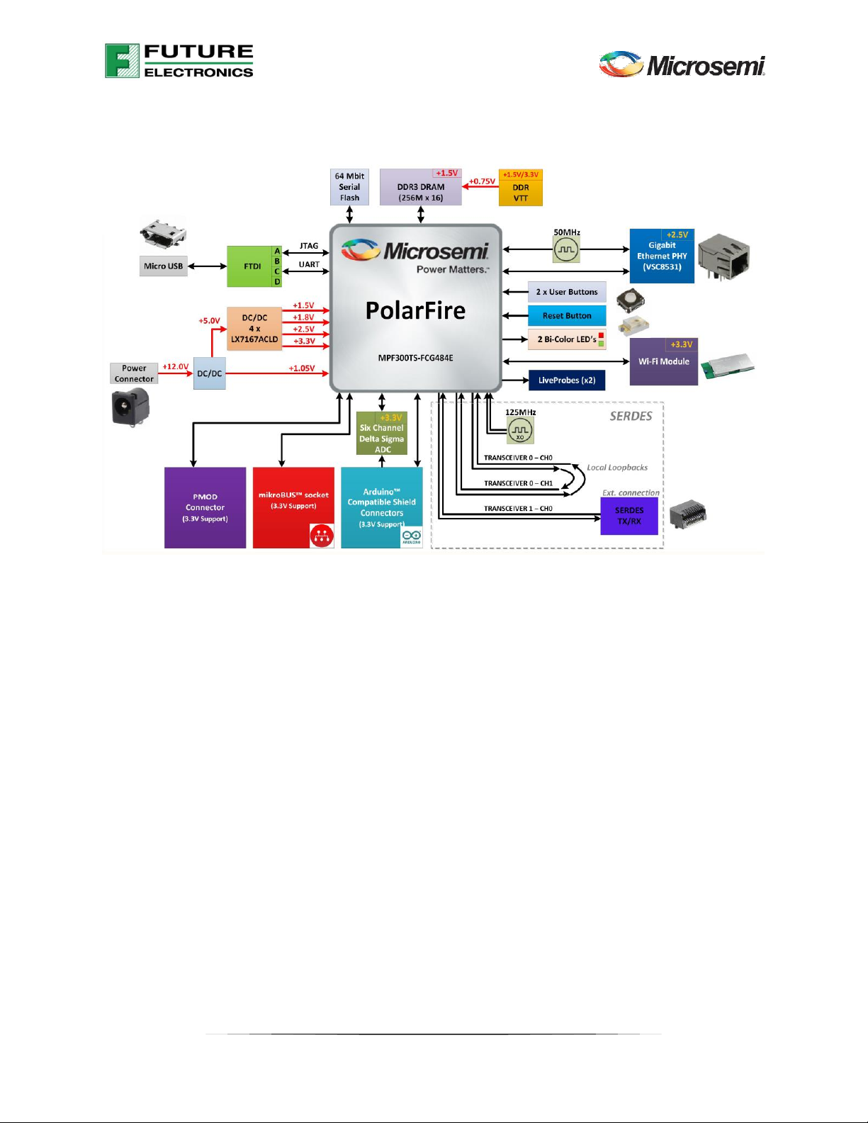
2.2 Block Diagram .................................................................................... 8
2.3 Board Overview .................................................................................. 8
2.4 Powering Up the Board ........................................................................ 11
3 Installation and Setting ............................................................................. 12
3.1 Software Settings ............................................................................... 12
3.2 Hardware Settings .............................................................................. 12
3.2.1 Power Supply LEDs ........................................................................ 12
3.2.2 Test Points ................................................................................. 12
3.2.3 Power Sources ............................................................................. 12
4 Board Components and Operations................................................................ 14
4.1 DDR3 Memory Interface........................................................................ 14
4.2 SPI Serial Flash .................................................................................. 14
4.3 Transceivers ..................................................................................... 15
4.3.1 XCVR0 Interface ........................................................................... 15
4.3.2 XCVR1 Interface ........................................................................... 16
4.3.3 125-MHz Transceiver Reference Clock ................................................. 16
4.4 Microsemi PHY (VSC8531) ..................................................................... 17
4.5 Panasonic Wi-Fi (PAN9320) .................................................................... 18
4.6 Microchip ADC (MCP3903) ..................................................................... 19
4.7 Programming .................................................................................... 19
4.7.1 FTDI ......................................................................................... 19
4.8 System Reset .................................................................................... 20
4.9 50-MHz Oscillator ............................................................................... 20
4.10 User Interface................................................................................... 21
4.10.1 User LEDs ................................................................................... 21
4.10.2 Push-Button Switches..................................................................... 21
4.10.3 Live Probes Header ....................................................................... 22
4.10.4 SFP+ Connector ............................................................................ 22

4.10.5 Arduino™ Compatible Expansion Headers.............................................. 23
4.10.6 MikroBUS™ Compatible Expansion Headers ............................................ 24
4.10.7 PMOD™ Compatible Expansion Connector ............................................. 25
5 Pin List................................................................................................. 26
6 Board Component Placement ...................................................................... 27
7 Demo Design .......................................................................................... 28
8 Appendix: Programming PolarFire FPGA Using the On-Board FlashPro5 ..................... 29

Figures
Figure 1 - Avalanche Block Diagram ..................................................................... 8
Figure 2 - Avalanche Board ............................................................................... 9
Figure 3 - Avalanche Board Power Supply Block diagram............................................ 13
Figure 4 - DDR3 Memory Interface ...................................................................... 14
Figure 5 - SPI Flash Interface ............................................................................ 15
Figure 6 - XCVR0 Interface ............................................................................... 15
Figure 7 - XCVR1 Interface ............................................................................... 16
Figure 8 - Transceiver Reference Clock ................................................................ 16
Figure 9 - PHY Interface.................................................................................. 17
Figure 10 - PAN9320 Block Diagram..................................................................... 18
Figure 11 - Wi-Fi Interface ............................................................................... 18
Figure 12 - ADC Interface ................................................................................ 19
Figure 13 - FTDI Interface ................................................................................ 20
Figure 14 - Reset Circuit.................................................................................. 20
Figure 15 - 50-MHz Clock Oscillator..................................................................... 21
Figure 16 - Live Probes Header.......................................................................... 22
Figure 17 - Silkscreen Top View ......................................................................... 27
Figure 18 - Silkscreen Botton View ..................................................................... 27
Figure 19 - Selecting the On-Board FlashPro5......................................................... 29

Tables
Table 1 - Avalanche Board Components................................................................ 10
Table 2 - Power Supply LEDs............................................................................. 12
Table 3 - I/O Voltage Rails ............................................................................... 12
Table 4 - Wi-Fi LEDs....................................................................................... 18
Table 5 - User LEDs........................................................................................ 21
Table 6 - Push-Button Switches ......................................................................... 21
Table 7 - J11 SFP+ Connector Pinout ................................................................... 23
Table 8 - J3 Arduino Connector Pinout................................................................. 23
Table 9 - J4 Arduino Connector Pinout................................................................. 23
Table 10 - J6 Arduino Connector Pinout ............................................................... 24
Table 11 - J7 Arduino Connector Pinout ............................................................... 24
Table 12 - J8 MikroBUS Connector Pinout ............................................................. 24
Table 13 - J9 MikroBUS Connector Pinout ............................................................. 25
Table 14 - J5 PMOD Connector Pinout.................................................................. 25

6
1Revision History
The revision history describes the changes that were implemented in the document. The
changes are listed by revision, starting with the most current publication.
1.1 Revision 1.0
Revision 1.0 is the first publication of this document.

7
2Getting Started
The Future Electronics - Microsemi Avalanche Development Kit (AVMPF300TS-02-NA/EU) is an
RoHS-compliant, cost optimized kit with general-purpose interfaces that enables you to
evaluate the basic features of the PolarFire family of FPGAs.
The Avalanche Development Kit supports the following interfaces:
2.4 GHz ISM band Wi-Fi module
1 GbE
DDR3 memory
SFP+ connector with one transceiver lane
Arduino™ compatible expansion headers
MikroBUS™ compatible expansion headers
PMOD™ compatible expansion connector
UART interface to FTDI device
SPI interface to SPI flash device
The PolarFire device is programmed using the on-board FlashPro5 programmer. The on-board
FlashPro5 programmer is used to develop and debug embedded applications using
SoftConsole, Identify, or SmartDebug.
2.1 Box Contents
The Avalanche Development Kit includes the following:
Future Electronics - Microsemi Avalanche Development Board featuring the MPF300TS-
1FCG484EES device with 300K logic elements
12V / 2A wall-mounted power adapter
USB-A to Micro B 2.0 cable for UART/JTAG interface to PC
The Avalanche Development Board Quick Start Guide
One-year Libero Gold software license

8
2.2 Block Diagram
The following block diagram shows all the components of the Avalanche Board.
Figure 1 - Avalanche Block Diagram
2.3 Board Overview
The Avalanche Board features a PolarFire MPF300TS-1FCG484EES FPGA with the following
capabilities:
20-Kb dual-port or two-port LSRAM block with a built-in single error correct double
error detect (SECDED) capability
64 × 12 two-port μSRAM block implemented as an array of latches
18 × 18 multiply-accumulate (MACC) block with a pre-adder, a 48-bit accumulator, and
an optional 16 deep × 18 coefficient RO
Built-in μPROM, modifiable at program time and readable at run time, for user data
storage
Digest integrity check for FPGA, μPROM, and sNVM
Low-power features:
oLow device static power
oLow inrush current
oLow power transceivers
oUnique Flash*Freeze mode
High-performance communication interfaces

9
The Avalanche Board supports several standard interfaces, including:
Microsemi VSC8531 with an RJ45 connector for 10/100/1000 Mbps Ethernet
One full-duplex transceiver lane connected through SFP+ connector
DDR3 memory
2.4 GHz ISM band using Panasonic PAN9320 Wi-Fi module
Arduino™ compatible expansion headers
MikroBUS™ compatible expansion headers
PMOD™ compatible expansion connector
One SPI flash device
The following illustration highlights various components of the Avalanche Board.
Figure 2 - Avalanche Board

10
The following table lists the important components of the Avalanche Board.
Component
Label on Board
Description
Feature Device
PolarFire FPGA
MPF300TS-1FCG484EES FPGA with data security.
Power Supply
12V power supply
input
J1
The board is powered by a 12V power source using an external
12 V / 2 A DC jack.
Clocks
50 MHz clock
oscillator
X2
50-MHz clock oscillator with single-ended output (± 50ppm).
125 MHz
differential clock
oscillator
X3
125-MHz oscillator with differential LVDS output (± 50ppm).
FPGA Programming and Debugging
USB-UART
terminal
J2
FTDI programmer interface to program the PolarFire device.
SPI Flash
U15
Microchip 64Mb serial flash SST26VF064B connected to bank 3
of the PolarFire device.
FT4232HL
U7
USB-to-quad serial ports in various configurations.
Live Probes
P4
To be used with SmartDebug
Communication Interfaces
SFP+ connector
J12
SFP connector on one XCVR lane to support the optical
interface with an external interface module
One 10/100/1000
Ethernet RJ45
connector
J10
Ethernet (RJ45) jack with external magnetics interfacing
with Microsemi 10/100/1000 BASE-T PHY (VSC8531) in
RGMII mode. The PHY interfaces with the Ethernet ports of
the PolarFire device.
Wi-Fi Module
MOD1A
Panasonic Pan9320 2.4 GHz ISM band module connected to
bank2 of the PolarFire device.
Arduino header
J3, J4, J6, J7
Connected to bank2
MikroBus header
J8, J9
Connected to bank2
PMod connector
J5
Connected to bank2
Memory
DDR3 Memory
U13
Microchip 64Mb serial flash SST26VF064B
Analog Interface
ADC
J6
Microchip analog converter A/D MCP3903 connected to bank2
of the PolarFire device. Analog inputs available through header
J6 (Arduino).
General Purpose I/O
Switches
SW1, SW2
Push-button switches for user-interface debugging
applications
Light-emitting
diodes
(LEDs)
LED1 to LED11
Two active-low dual colors LEDs connected to some of the user
I/Os for debugging, one active low LED for reset, three active
high LEDs used for indicating power supply and five active high
LEDs used for Wi-Fi module statuses.
Reset switch
SW3
Push-button system reset for the PolarFire device. Users
must program this GPIO for PolarFire device reset
function.
Table 1 - Avalanche Board Components

11
2.4 Powering Up the Board
The Avalanche Board can only be powered up using the 12 V DC jack.

12
3Installation and Setting
This section provides information about the software and hardware settings required to run
the pre-programmed demo design on the Avalanche Board.
3.1 Software Settings
Download and install the latest release of Microsemi Libero® SoC PolarFire software from the
Microsemi website, and register for a free one-year Gold License to the Libero software. The
Libero SoC PolarFire installer includes FlashPro5 drivers. For instructions about installing
Libero SoC PolarFire and SoftConsole, see the Libero Software Installation and Licensing
Guide. For instructions about how to download and install Microsemi DirectCores and driver
firmware cores on the PC where Libero SoC is installed, see the Installing IP Cores and Drivers
User’s Guide.
3.2 Hardware Settings
This section provides information about LEDs, test points and power supply structure on the
Avalanche Board.
3.2.1 Power Supply LEDs
The following table lists the power supply LEDs on the Avalanche Board.
LED
Description
LED1
5.0 V rail
LED2
3.3V rail
LED3
5.0 V rail (USB)
Table 2 - Power Supply LEDs
3.2.2 Test Points
The following test points available on the Avalanche Board:
TP1, TP2: headers
TP3 to TP18
Refer to the schematic for more details.
3.2.3 Power Sources
The following table lists the key power supplies required for normal operation of the
Avalanche Board.
PolarFire Bank
I/O Rail
Voltage
Bank 0, 1
VDD15
1.5 V
Bank 2
3P3V
3.3 V
Bank 3
3P3V
3.3 V
Bank 4
VDD25
2.5 V
Table 3 - I/O Voltage Rails

13
The following figure shows voltage rails (12 V, 5 V, 3.3 V, 2.5 V, 1.8 V, 1.5 V, 1.05 V and 0.9
V) available on the Avalanche Board.
Figure 3 - Avalanche Board Power Supply Block diagram

14
4Board Components and Operations
This section describes the key components of the Avalanche Board and provides information
about important board operations.
4.1 DDR3 Memory Interface
One 4-Gb DDR3 SDRAM chip is provided to serve as flexible volatile memory for user
applications. The DDR3 interface is implemented in HSIO bank0 and bank1.
The DDR3 SDRAM specifications for the PolarFire device are:
One AS4C256M16D3A-12BIN chip connected in fly-by topology.
Density: 512 MB
Data rate: DDR3 16-bit up to 133 MHz clock rate
The DDR3 memory can operates up to 1066 MHz with gearing 1:4 for the 133-MHz PolarFire
fabric implementing a RISC-V system per example. The default board assembly available for
the DDR3 standard has RC terminations.
Figure 4 - DDR3 Memory Interface
For more information, see the Board Level Schematics document (provided separately).
4.2 SPI Serial Flash
The SPI flash specifications for the PolarFire device are:
Density: 64 Mb
Voltage: 2.7 V to 3.6 V (SST26VF064B)
Frequency: 104 MHz
Quantity: 1
SPI mode support : Modes 0 and 3
Dedicated bank: Bank3

15
Figure 5 - SPI Flash Interface
For more information, see the Board Level Schematics document (provided separately).
4.3 Transceivers
The PolarFire MPF300TS-1FCG484EES device has sixteen transceiver lanes, which can be
accessed through a PCB loopback and the SPF+ connector on the board.
4.3.1 XCVR0 Interface
The XCVR0 interface has two lanes connected as follows:
Lanes 0 and 1 are directly routed together to form a loopback
The XCVR0 reference clock is routed directly from the 125 MHz differential clock oscillator to
the PolarFire device.
The XCVR0 TXD pairs are capacitive coupled to the PolarFire device. Serial AC-coupling
capacitors are used to provide common-mode voltage independence.
The following figure shows the XCVR0 interface of the Avalanche Board.
Figure 6 - XCVR0 Interface
PolarFire FPGA
BANK3
SPI Flash
(64 Mb)
DO
DI
CS
Clk
PolarFire FPGA
Lane 0 / RXD
Lane 1 / RXD
Lane 0 / TXD
Lane 1 / TXD
XCVR_0A-REFCLK
125 MHz
Clock

16
4.3.2 XCVR1 Interface
The XCVR1 interface has one lane that is connected to the SFP+ connector. The signals are
routed in the PCB as follows:
Lanes 0 is directly routed to the SFP+ connector.
The XCVR0 reference clock can be used with the XCVR1 interface.
The following figure shows the XCVR1 interface of the Avalanche Board.
Figure 7 - XCVR1 Interface
4.3.3 125-MHz Transceiver Reference Clock
A 125-MHz clock oscillator with an accuracy of +/-50 ppm is available on the board. This clock
oscillator is connected to the FPGA fabric to provide transceiver reference clock.
The transceiver supports reference clock connected as follows:
XCVR 0A reference clock is connected the on-board 125-MHz oscillator.
The following figure shows the XCVR reference clock interface of the Avalanche Board.
Figure 8 - Transceiver Reference Clock
PolarFire FPGA
Controls
Lane 0 / RXD
Lane 0 / TXD
XCVR_0A-REFCLK
125 MHz
Clock
SFP+
Controls
TX
RX
PolarFire FPGA
XCVR_0A-REFCLK
125 MHz
Clock

17
4.4 Microsemi PHY (VSC8531)
The Microsemi VSC8531 device is designed for space-constrained 10/100/1000BASE-T
applications. It features integrated, line-side termination to conserve board space, lower EMI,
and improve system performance. Additionally, integrated RGMII timing compensation
eliminates the need for on-board delay lines.
Microsemi EcoEthernet™ 2.0 technology supports IEEE 802.3az Energy-Efficient Ethernet (EEE)
and power-saving features to reduce power based on link state and cable reach. VSC8531
optimizes power consumption in all link operating speeds and features a Wake-on-LAN (WoL)
power management mechanism for bringing the PHY out of a low-power state using
designated magic packets.
The following figure shows the PHY interface of the Avalanche Board.
Figure 9 - PHY Interface
PolarFire FPGA
GPIO –Bank 4
50 MHz
Crystal
VSC8531
PHY
ETH_TXD[0:3]
ETH_RXD[0:3]
Port 0
RJ 45
MDC/MDIO

18
4.5 Panasonic Wi-Fi (PAN9320)
The Panasonic PAN9320 is a 2.4 GHz ISM band Wi-Fi-embedded module which includes a
wireless radio and an MCU for easy integration of Wi-Fi connectivity into various electronic
devices.
Figure 10 - PAN9320 Block Diagram
The following table shows the different status LEDs of the Wi-Fi Module.
Avalanche Board
Reference
Description
LED 6
Wireless (Wi-Fi) status, active low
LED 7
Error (active during booting), active low
LED 8
IP connectivity (allocated IP), active low
LED 9
MCU status (heartbeat), active low
LED 10
MCU ready (booting ready), active high
Table 4 - Wi-Fi LEDs
The following figure shows the Wi-Fi Module interface.
Figure 11 - Wi-Fi Interface
PolarFire FPGA
GPIO –Bank 2
PAN9320 Wi-
Fi
UART 0
UART 1
Controls
Commands
Data

19
4.6 Microchip ADC (MCP3903)
The Microchip MCP3903 is a six-channel Analog Front End (AFE) containing three pairs made
out of two synchronous sampling Delta-Sigma Analog-to-Digital Converters (ADC) with PGA, a
phase delay compensation block, internal voltage reference, and high-speed 10 MHz SPI
compatible serial interface. The converters contain a proprietary dithering algorithm for
reduced idle tones and improved THD.
The following figure shows the A/D Converter interface.
Figure 12 - ADC Interface
4.7 Programming
The PolarFire device is programmed using the on-board FlashPro5 programmer. For more
information about how to program the device, see Appendix: Programming PolarFire FPGA
Using the On-Board FlashPro5, page 29.
4.7.1 FTDI
The key features of the FT4232HL chip are:
USB 2.0 high-speed (480 Mbps) to UART/MPSSE IC
Single-chip USB-to-quad serial ports in various configurations
Entire USB protocol handled on the chip without requiring USB-specific firmware
programming
USB 2.0 high-speed (480 Mbps) and full-speed (12 Mbps) compatibility
Two multi-protocol synchronous serial engines (MPSSE) on channel A and channel B to
simplify synchronous serial protocol (USB to JTAG, I2C, SPI, or bit-bang) design
Note: FTDI chip requires 1.8 V chip core voltage and +3.3 V I/O voltage
PolarFire FPGA
GPIO –Bank 2
MCP3903 ADC
Controls
SDI
SDO
SCK
Arduino
J6
Channels
0 to 5
Mikro
J8
Channel 0

20
Figure 13 - FTDI Interface
The EEPROM that is connected to the FTDI device is programmed so that Port A of the FTDI
device is recognized as an embedded FlashPro5.
The FTDI USB to serial device provides four separate interfaces. Port A is used for a JTAG
connection to the FPGA, Port C is used as a UART interface to the FPGA. Ports B and D are
unused. When connecting a computer to the baseboard, four separate COM ports are
recognized. The third port in the group of four will be the UART port. This is important when
using a console port program such as HyperTerm or TeraTerm.
4.8 System Reset
DEVRST_N is an input-only reset pad that allows a full reset of the chip to be asserted at any
time. The following figure shows a sample reset circuit that uses a Microchip MCP121T-
240E/TT device
Figure 14 - Reset Circuit
Note: For the User Reset option, please see section 4.10.2
4.9 50-MHz Oscillator
A 50-MHz clock oscillator with an accuracy of +/-50 ppm is available on the board. This clock
oscillator is connected to the FPGA fabric and to Microsemi PHY to provide a system reference
clock to both devices.
An on-chip PolarFire phase-locked loop (PLL) can be configured to generate a wide range of
high-precision clock frequencies.
The pins number of the 50-MHz oscillator are:
PolarFire
FPGA
FTDI
FT4232
UART
Port A
EEPROM
Mini USB
J2
JTAG
Port C
ESD
Table of contents
Other Future Electronics Motherboard manuals