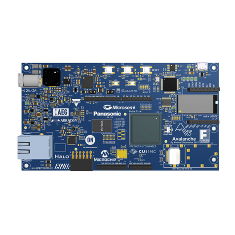
Future Electronics Microsemi User manual

Future Electronics - Microsemi
Creative Development Board
User Guide - Rev. 1

Page 2 – Revision 1
Table of Contents
Introduction . . . . . . . . . . . . . . . . . . . . . . . . . . . . . . . . . . . . . . . . . . . . . . . . . . . 3
Contents and System Requirements . . . . . . . . . . . . . . . . . . . . . . . . . . . . . . . 4
Hardware Components . . . . . . . . . . . . . . . . . . . . . . . . . . . . . . . . . . . . . . . . . . 5
PLL Parts/Usage . . . . . . . . . . . . . . . . . . . . . . . . . . . . . . . . . . . . . . . . . . . . . . . 7
Power Supplies . . . . . . . . . . . . . . . . . . . . . . . . . . . . . . . . . . . . . . . . . . . . . . . . 8
Mini USB Connector for Power, JTAG and UART Connectivity . . . . . . . . . . 10
Programming or Re-Programming the Example Design. . . . . . . . . . . . . . . . 11
Clock Circuits . . . . . . . . . . . . . . . . . . . . . . . . . . . . . . . . . . . . . . . . . . . . . . . . 11
Differential I/O Standards . . . . . . . . . . . . . . . . . . . . . . . . . . . . . . . . . . . . . . . 11
Setup and Running Out-of-the-box demo . . . . . . . . . . . . . . . . . . . . . . . . . . 12
Package Connections . . . . . . . . . . . . . . . . . . . . . . . . . . . . . . . . . . . . . . . . . . 13
Memory Setups . . . . . . . . . . . . . . . . . . . . . . . . . . . . . . . . . . . . . . . . . . . . . . . 17
Schematics – Connectors . . . . . . . . . . . . . . . . . . . . . . . . . . . . . . . . . . . . . . . 18
– FTDI-JTAG . . . . . . . . . . . . . . . . . . . . . . . . . . . . . . . . . . . . . . . 20
– DDR SDRAM. . . . . . . . . . . . . . . . . . . . . . . . . . . . . . . . . . . . . . 22
– FPGA IO . . . . . . . . . . . . . . . . . . . . . . . . . . . . . . . . . . . . . . . . . 24
– FPGA Power-PLL . . . . . . . . . . . . . . . . . . . . . . . . . . . . . . . . . . 26
– Power Supplies. . . . . . . . . . . . . . . . . . . . . . . . . . . . . . . . . . . . 28

Page 3 – Revision 1
Introduction
Thank you for purchasing the Future Electronics - Microsemi Creative Development Board. This
guide provides the information required to easily evaluate the board.
Document Assumptions
This user’s guide assumes:
• You intend to use the Microsemi SoC Products Group Libero® System-on-Chip (SoC) suite.
• You have installed and are familiar with Microsemi SoC Products Group Libero SoC v10.0
or later.
• You are familiar with PCs and the Windows® operating system.
Additional Information
Refer to the Libero SoC Quick Start Guide to get familiar with the Microsemi SoC Products Group
FPGA development flow using Libero SoC.

Page 4 – Revision 1
Contents and System Requirements
This chapter details the contents of the Creative Development Board and lists the power supply and
software system requirements.
Box Contents
The Starter Kit includes the following:
• Future Electronics - Microsemi Creative Development Board
• The Creative Development Board Quick Start Guide
• USB Cable

Page 5 – Revision 1
Hardware Components
This chapter describes the hardware components of the Creative Development Board.
Creative Development Board
Figure 2-1 illustrates a top-level view of the Creative Development Board. The Creative Development
Board consists of the following:
• Microsemi IGLOO2 (M2GL025) or SmartFusion2 (M2S025) FPGA
• Microsemi DC-DC LX7167
• Alliance 32M x 16-bit DDR2 synchronous DRAM (SDRAM)
• Microchip 64Mb serial flash
• Microchip six synchronous sampling 16/24-bit resolution Delta-Sigma A/D converters
• On-board FTDI USB-JTAG adaptor (FlashPro5)
• Arduino™ compatible expansion headers
• MikroBUS™ compatible expansion headers
• PMOD™ compatible expansion connector
• User buttons and LED
Detailed Board Description and Usage
The Creative Development board has various advanced features that are covered in later sections of
this chapter. This board is socketed and is populated with SmartFusion2 FPGA (M2S025) or IGLOO2
FPGA (MSGL025).

Page 6 – Revision 1
Power
Matters.
™
S
martFusion
®
2
I
GLOO
®
2
FPGA
User buttonsPMod connectors
64 Mbit Serial Flash512 Mb DDR2 SDRAM Arduino connectors
Arduino connectorsA/D Converter
Microsemi FPGA
FTDI USB-JTAGUSB
LEDs
mikroBUS
connectors
Hardware Components
Full schematics are available for download from the Future Electronics website:
http://www.futureelectronics.com/en/campaign/microsemi/Pages/CreativeDevelopmentBoard.aspx
The electronic versions of the dedicated schematics can be enlarged to a far greater degree than
shown in the printed version of this manual or even in the electronic version of this manual, hence
the interested reader is referred to the dedicated schematics to see the appropriate level of detail.
Figure 2-1 • Creative Development Board

Page 7 – Revision 1
PLL Parts/Usage
Instructions for PLL on Creative Development Board
IGLOO2 and SmartFusion2 M2GL025 devices have up to six fabric CCC (FAB_CCC) blocks at 3.3V
and a dedicated PLL associated with each CCC to provide flexible clocking to the FPGA fabric
portion of the device. The user has the freedom to use any of the eight PLLs and CCCs to generate
the fabric clocks and the internal HPMS clock from the base fabric clock (CLK_BASE). There is
also a dedicated CCC block for the HPMS (HPMS_CCC) and an associated PLL (MPLL) for HPMS
clocking and de-skewing the CLK_BASE clock. The fabric alignment clock controller (FACC), part
of the HPMS CCC, is responsible for generating various aligned clocks required by the HPMS for
correct operation of the HPMS blocks and synchronous communication with the user logic in the
FPGA fabric.

Page 8 – Revision 1
Mini USB Connector for Power, JTAG and UART Connectivity
The Mini USB Connector is used to power the BB as well as provide an embedded FlashPro5
interface to the Microsemi Libero and SoftConsole tools. More information and downloads for Libero
and SoftConsole can be found here:
http://www.microsemi.com/products/fpga-soc/design-resources/design-software
The mini USB can power the board up to 500mA. The EEPROM that is connected to the FTDI device
ss programmed so that Port A of the FTDI device is recognized as an embedded FlashPro5.
The FTDI USB to serial device provides four separate interfaces. Port A is used for a JTAG
connection to the FPGA, Port C is used as a UART interface to the FPGA. Ports B and D are
unused. When connecting a computer to the baseboard, four separate COM ports are recognized.
The third port in the group of four will be the UART port. This is important when using a console port
program such as HyperTerm or TeraTerm.
FTDI
FT4232
Mini USB
ESD
To Power Block
Port A
Port C UART
JTAG
EEPROM
Igloo2
SmartFusion2

Page 9 – Revision 1
Power Supplies
3.3V DC-DC
1.2V DC-DC

Page 10 – Revision 1
Power Supplies
1.8V DC-DC
0.9V for DDR

Page 11 – Revision 1
Programming or Re-Programming the Example Design
Download the latest version of the Creative Development example design from the Future
Electronics website:
http://www.futureelectronics.com/en/campaign/microsemi/Pages/CreativeDevelopmentBoard.aspx
Clock Circuits
IGLOO2/SmartFusion2 devices have two on-chip RC oscillators—a 1 MHz RC oscillator and a 50
MHz RC oscillator—and up to two main crystal oscillators (32 kHz–20 MHz). These are available to
the user for generating clocks to the on-chip resources and the logic built on the FPGA fabric array.
The second crystal oscillator available on the SmartFusion2 devices is dedicated for RTC clocking.
These oscillators (except the RTC crystal oscillator) can be used in conjunction with the integrated
user phase-locked loops (PLLs) and fabric clock conditioning circuits (FAB_CCC) to generate clocks
of varying frequency and phase. In addition to being available to the user, these oscillators are also
used by the system controller, power-on reset circuitry, MSS during Flash*Freeze mode, and the RTC.
Differential I/O Standards
Configuration of the I/O modules as a differential pair is handled by Microsemi SoC Products Group
Libero software when the user instantiates a differential I/O macro in the design. Differential I/Os
can also be used in conjunction with the embedded Input register (InReg), Output register (OutReg),
Enable register (EnReg), and Double Data Rate registers (DDR). These differential signals are brought
out to the PMOD interface. The differential pairs for the PMOD are in the BANK2 with 4 differential
signal @ 3.3V.

Page 12 – Revision 1
Setup and Running Out-of-the-box demo
Software Installation
Tools are available for download at http://www.microsemi.com/products/fpga-soc/design-resources/
design-software/libero-soc#downloads. You can download either Windows or Linux Libero SoC
development software. Following are instructions for Windows:
• Download and install the latest revision of Libero SoC (and Service Packs) by following
Libero SoC – InstallShield Wizard
License Installation
In order to run Libero SoC, you must first request then install a license.
• Request a free license by logging in to Microsemi SoC Portal
https://soc.microsemi.com/portal/default.aspx?r=1
• Answer all the survey questions
• Select Libero Gold Node Locked for Windows. Your license will arrive by email.
• To install a Node Locked disk ID license in Windows, add or update your LM_LICENSE_FILE
environment variable so it points to the new License.dat file by following the instruction
found in: http://www.microsemi.com/document-portal/doc_view/131602-libero-software-
installation-and-licensing-guide
For more information, to get schematics, software, guides etc., please register and download:
http://www.FutureElectronics.com/CreativeDevelopmentBoard
Running the Out-of-Box Demo
To power up the device out of the box, connect the board via USB Power Connector, as shown in
the picture below, to a USB power source such as a computer. By default, the Green LED will start
blinking slowly every 1 second while the Red LED will blink every 2 seconds.
• Press and hold Switch 1, the Green LED will
start blinking faster (every 0.5 second)
• Press and hold Switch 2, the Red LED will
start blinking faster (every 1 second)
Power
Matters.
™
S
martFusion
®
2
I
GLOO
®
2
FPGA
Reset Red LEDSwitch 1
Green LEDSwitch 2
USB Power
Connector

Page 13 – Revision 1
Package Connections
mikroBUSTM Adaptor
J5 Function FPGA Pin Pin Name Voltage
1 AD_CH0 U6(2) A/D Converter MCP3903-E/SS CH0 5.0V Max
2 MIKRO_RST R11 MSIO134NB4 3.3V
3 MIKRO_CS T12 MSIO138PB4 3.3V
4 MIKRO_SCK R12 MSIO138NB4 3.3V
5 MIKRO_MISO T13 MSIO145PB4 3.3V
6 MIKRO_MOSI R13 MSIO145NB4 3.3V
7 +3.3V – – –
8 GND – – –
J6
1 MIKRO_PWM R10 MSIO131NB4 3.3V
2 MIKRO_INT R9 MSIO130NB4 3.3V
3 MIKRO_RX R8 MSIO126PB4 3.3V
4 MIKRO_TX T8 MSIO122NB4 3.3V
5 MIKRO_SCL T7 MSIO122PB4 3.3V
6 MIKRO_SDA R6 MSIO120PB4 3.3V
7 +5.0V_USB – – –
8 GND – – –
ArduinoTM Connectors
J1 Function FPGA Pin Pin Name Voltage
1 NC – VIN –
2 GND – – –
3 GND – – –
4 +5.0V_USB – – –
5 +3.3V – IOREF –
6 ARD_RESET G1 MSIO97PB7/GB2/CCC_NW0_CLKI1 3.3V
7 +3.3V – – –
8 NC – – –
J2
1 ARD_IO0 P6 MSIO121PB4/PROBE_A 3.3V
2 ARD_IO1 P7 MSIO121NB4/PROBE_B 3.3V
3 ARD_IO2 N7 MSIO125NB4/GB7/CCC_SW1_CLKI2 3.3V
4 ARD_IO3 M7 MSIO125PB4/GB3/CCC_SW0_CLKI3 3.3V
5 ARD_IO4 P8 MSIO126NB4 3.3V
6 ARD_IO5 M8 MSIO129NB4 3.3V
7 ARD_IO6 N8 MSIO129PB4/CCC_SW1_CLKI3 3.3V
8 ARD_IO7 P9 MSIO131PB4/GB11/VCCC_SE0_CLKI 3.3V
J4
1 AD_CH0 U6(2) A/D Converter MCP3903-E/SS CH0 5.0V Max
2 AD_CH1 U6(5) A/D Converter MCP3903-E/SS CH1 5.0V Max
3 AD_CH2 U6(6) A/D Converter MCP3903-E/SS CH2 5.0V Max
4 AD_CH3 U6(9) A/D Converter MCP3903-E/SS CH3 5.0V Max
5 AD_CH4 U6(10) A/D Converter MCP3903-E/SS CH4 5.0V Max
6 AD_CH5 U6(13) A/D Converter MCP3903-E/SS CH5 5.0V Max
J7
1 ARD_IO8 M9 MSIO132PB4 3.3V
2 ARD_IO9 M10 MSIO132NB4 3.3V
3 ARD_IO10 N10 MSIO133NB4 3.3V
4 ARD_IO11 P10 MSIO133PB4/GB15/VCCC_SE1_CLKI 3.3V
5 ARD_IO12 P12 MSIO143PB4 3.3V
6 ARD_IO13 P13 MSIO143NB4 3.3V
7 GND – – –
8 ARD_AVREF – +3.3V –
9 ARD_SDA T9 MSIO130PB4/VCCC_SE0_CLKI 3.3V
10 ARD_SCL T6 MSIO120NB4/CCC_SW0_CLKI2 3.3V

Page 14 – Revision 1
PMod Connectors
J8 Function FPGA Pin Pin Name Voltage
1 PMOD_D0_P L11 MSIO3PB2 3.3V
2 PMOD_D0_N L12 MSIO3NB2 3.3V
3 PMOD_D1_P L14 MSIO5PB2 3.3V
4 PMOD_D1_N L13 MSIO5NB2 3.3V
5 PMOD_D2_P N14 MSIO2PB2 3.3V
6 PMOD_D2_N M13 MSIO2NB2 3.3V
7 PMOD_D3_P M15 MSIO0PB2 3.3V
8 PMOD_D3_N N15 MSIO0NB2 3.3V
9 GND – – –
10 GND – – –
11 +3.3V – – –
12 +3.3V – – –
A/D Converter
U6 Function FPGA Pin Pin Name Voltage
18 ADC_DR_N H4 MSIO99NB7 3.3V
21 ADC_CLK_IN F4 MSIO96PB7/GB6/CCC_NW1_CLKI1 3.3V
23 ADC_CS_N G2 MSIO98NB7 3.3V
24 ADC_SCK F2 MSIO97NB7 3.3V
25 ADC_SDO F3 MSIO96NB7 3.3V
26 ADC_SDI F5 MSIO95NB7 3.3V
27 ADC_RST G5 MSIO95PB7 3.3V
LED and User Buttons
Function FPGA Pin Pin Name Level
LED1_GREEN J16 MSIO11PB2//CCC_NE0_CLKI0 Active High
LED1_RED K16 MSIO4PB2 Active High
LED2_GREEN M16 MSIO1NB2 Active High
LED2_RED N16 MSIO1PB2 Active High
USER_BUTTON1 H12 MSIO27NB1 Active High
USER_BUTTON2 H13 MSIO28NB1 Active High
64 Mbit Serial Flash (SST26VF064B-104I/SM)
U10 Function PFGA Pin Pin Name
1 CE J12 MSIO13NB2/SPI_0_SS0
2 S0 J13 MSIO12NB2/SPI_0_SDI
3 WP H14 MSIO15PB2/SPI_0_SS6
4 GND – VSS
5 SI K12 MSIO13PB2/SPI_0_SDO
6 CLK J14 MSIO12PB2/SPI_0_CLK
7 HOLD G16 MSIO14NB2/SPI_0_SS5
8 +3.3V – VDDI7

Page 15 – Revision 1
32Mx16 DDR2 Synchronous RAM ( AS4C32M16D2A-25BCN )
U3 Function PFGA Pin Pin Name
A1 +1.8V – +1.8V
A2 NC – NC
A3 GND A6 GND
A7 GND A6 GND
A8 MDDR_UDQS_N A10 DDRIO52NB0/MDDR_DQS1_N
A9 +1.8V – +1.8V
B1 MDDR_DQ14 D9 DDRIO49PB0/MDDR_DQ14/CCC_NE1_CLKI3
B2 GND – GND
B3 MDDR_UDQM C10 DDRIO51NB0/MDDR_DM_RDQS1
B7 MDDR_UDQS_P A9 DDRIO52PB0/MDDR_DQS1/GB8/CCC_NE0_CLKI3
B8 GND – GND
B9 MDDR_DQ15 E8 DDRIO49NB0/MDDR_DQ15
C1 +1.8V – +1.8V
C2 MDDR_DQ9 C9 DDRIO54NB0/MDDR_DQ9
C3 +1.8V – +1.8V
C7 +1.8V – +1.8V
C8 MDDR_DQ8 C8 DDRIO54PB0/MDDR_DQ8
C9 +1.8V – +1.8V
D1 MDDR_DQ12 B11 DDRIO50PB0/MDDR_DQ12/GB12/CCC_NE1_CLKI2
D2 GND – GND
D3 MDDR_DQ11 D8 DDRIO53NB0/MDDR_DQ11
D7 MDDR_DQ10 D7 DDRIO53PB0/MDDR_DQ10/CCC_NE0_CLKI2
D8 GND A6 VSS
D9 MDDR_DQ13 B10 DDRIO50NB0/MDDR_DQ13
E1 +1.8V – +1.8V
E2 NC – NC
E3 GND – GND
E7 GND – GND
E8 MDDR_LDQS_N A4 DDRIO58NB0/MDDR_DQS0_N
E9 +1.8V – +1.8V
F1 MDDR_DQ6 C6 DDRIO56NB0/MDDR_DQ6
F2 GND – GND
F3 MDDR_LDQM A3 DDRIO57PB0/MDDR_DM_RDQS0
F7 MDDR_LDQS_P A5 DDRIO58PB0/MDDR_DQS0
F8 GND – GND
F9 MDDR_DQ7 A7 DDRIO55PB0/MDDR_DQ7
G1 +1.8V – +1.8V
G2 MDDR_DQ1 A2 DDRIO60NB0/MDDR_DQ1
G3 +1.8V – +1.8V
G7 +1.8V – +1.8V
G8 MDDR_DQ0 B2 DDRIO60PB0/MDDR_DQ0
G9 +1.8V A1 +1.8V
H1 MDDR_DQ4 B3 DDRIO57NB0/MDDR_DQ4
H2 GND – GND

Page 16 – Revision 1
32Mx16 DDR2 Synchronous RAM ( AS4C32M16D2A-25BCN )
U3 Function PFGA Pin Pin Name
H3 MDDR_DQ3 B5 DDRIO59NB0/MDDR_DQ3
H7 MDDR_DQ2 B6 DDRIO59PB0/MDDR_DQ2
H8 GND – GND
H9 MDDR_DQ5 B7 DDRIO56PB0/MDDR_DQ5
J1 +1.8V – +1.8V
J2 DDR_0.9V J2 DDP 0.9V Reference
J3 GND – GND
J7 GND – GND
J8 MDDR_CLK_P A14 DDRIO45PB0/MDDR_CLK
J9 +1.8V – +1.8V
K2 MDDR_CKE E10 DDRIO47PB0/MDDR_CKE
K3 MDDR_WE_N C11 DDRIO48NB0/MDDR_WE_N
K7 MDDR_RAS_N B12 DDRIO48PB0/MDDR_RAS_N
K8 MDDR_CLK_N A15 DDRIO45NB0/MDDR_CLK_N
K9 MDDR_ODT F16 DDRIO39PB0/MDDR_ODT
L1 NC – NC
L2 MDDR_BA0 C12 DDRIO44PB0/MDDR_BA0
L3 MDDR_BA1 D12 DDRIO44NB0/MDDR_BA1
L7 MDDR_CAS_N A12 DDRIO46NB0/MDDR_CAS_N
L8 MDDR_CS_N D11 DDRIO47NB0/MDDR_CS_N
M2 MDDR_A10 E14 DDRIO37PB0/MDDR_ADDR10
M3 MDDR_A1 E11 DDRIO42PB0/MDDR_ADDR1
M7 MDDR_A2 E12 DDRIO42NB0/MDDR_ADDR2
M8 MDDR_A0 C14 DDRIO43NB0/MDDR_ADDR0
M9 +1.8V – +1.8V
N1 GND – GND
N2 MDDR_A3 B16 DDRIO41PB0/MDDR_ADDR3
N3 MDDR_A5 D16 DDRIO40PB0/MDDR_ADDR5
N7 MDDR_A6 E16 DDRIO40NB0/MDDR_ADDR6
N8 MDDR_A4 C16 DDRIO41NB0/MDDR_ADDR4
P2 MDDR_A7 F15 DDRIO39NB0/MDDR_ADDR7
P3 MDDR_A9 E15 DDRIO38NB0/MDDR_ADDR9
P7 MDDR_A11 F13 DDRIO37NB0/MDDR_ADDR11
P8 MDDR_A8 F14 DDRIO38PB0/MDDR_ADDR8
P9 GND – GND
R1 +1.8V – +1.8V
R2 MDDR_A12 D14 DDRIO36PB0/MDDR_ADDR12
R3 NC – NC
R7 NC – NC
R8 NC – NC

Page 17 – Revision 1
Memory Setup

Page 18 – Revision 1
Schematics – Connectors
Arduino Connectors
Mikro Bus Adaptor

Page 19 – Revision 1
RESET PMOD Connector
USER Buttons and LEDs
Six Channel Delta Sigma A/D Convertor

Page 20 – Revision 1
Schematics – FTDI-JTAG
FTDI USB-JTAG
Table of contents
Other Future Electronics Motherboard manuals