I. DESCRIPTION
The
HAL
Communications Corp. I
D-1
A repeater identifier
is
designed
to
help owners
of
repeater
stations meet
FCC
requirements
for
periodic station identification.
It
automatically transmits the
station call sign at the required intervals whenever the repeater
is
in
use.
The I
D-1
A offers
these
advanced features:
•
TTL
integrated circuits
for
high noise
immunity
and wide operating temperature range
• Reprogrammable diode-matrix read-only memory
for
storage
of
the station call
sign
• Accurate interval
timing
derived
from
the AC power line
• Interval
timing
source
for
emergency
or
portable operation
from
DC
power
• Transistor switch
for
direct
control
of
the repeater keying relay
•
Page
control
input
to
inhibit
identification during paging tones
• Adjustable code
speed
• Low-impedance audio
output
with
adjustments
for
pitch and volume
• Regulated 5
volt
DC
power supply
•
Rugged
G-10 epoxy-glass
circuit
board
Operation
The I
D-1
A identifier
is
completely automatic.
It
senses
when the repeater
has
been actuated
and
immediately transmits the station call sign
by
feeding a keyed audio tone
to
the repeater trans-
mitter.
After
this initial identification
has
been sent, a short
"guard"
period commences.
At
the
same
time,
a three-minute
timing
interval starts.1
If
the repeater
is
again
keyed up during the guard period,
but
remains inactive during the nominal three-minute
timing
interval,
only
the initial identification
is
transmitted. This feature prevents the unnecessary repetition
of
the call
sign
if
the repeater
is
trig-
gered
briefly
by a noise burst
or
by
a short call
to
which there
is
no response.
If,
however, the repeater
is
reactivated after the guard period
but
before the
end
of
the timing
interval, the identifier
will
repeat the call sign
at
the end
of
the longer interval. The identification
will
be
transmitted approximately every three minutes
as
long
as
the repeater
is
activated once
during
each
interval.
If
the repeater
is
held continuously activated, the I
D-1
A
will
identify
at three
minute intervals.
If
the repeater happens
to
be
off
the air
at
the moment the identification
is
to
be
transmitted, a keying transistor
in
the I
D-1
A actuates the repeater keying relay, returning the trans-
mitter
to
the air while the call sign
is
being sent.
Identification may
be
inhibited
by
grounding the
page
control input.
If
this line
is
grounded when
the
timing
interval ends, identification will be delayed
until
the control line
is
released.
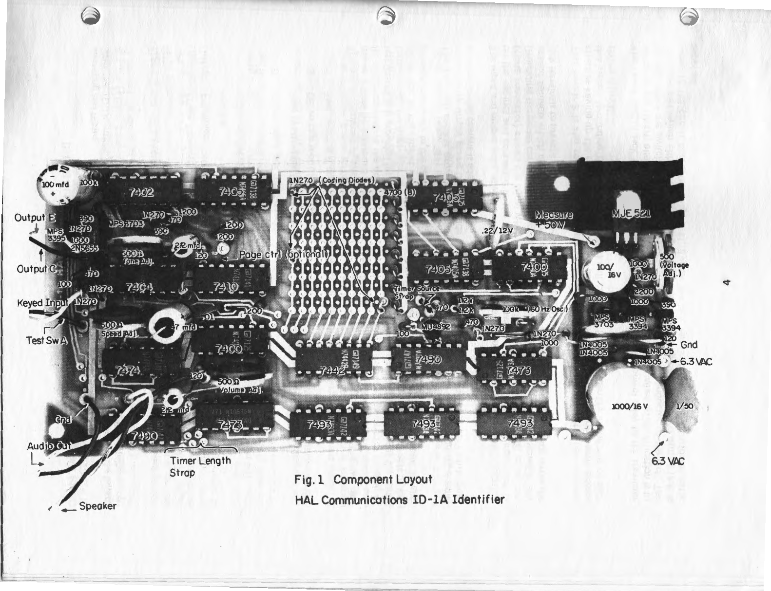
Circuit
Description
The identification
message
is
stored in a diode-matrix read-only memory (ROM). This memory
has
been
specially designed
to
store code characters (dots,
dashes,
or
spaces)
using a
minimum
number
of
diodes. The memory capacity
is
sufficient
to
store the letters
"DE"
plus any amateur call
sign.
1Timing intervals
of
approximately 6, 12,
or
24
minutes may also
be
selected
by
changing the position
of
ajumper
on the
circuit
board,
as
shown in the schematic diagram. The guard period remains the
same.
1