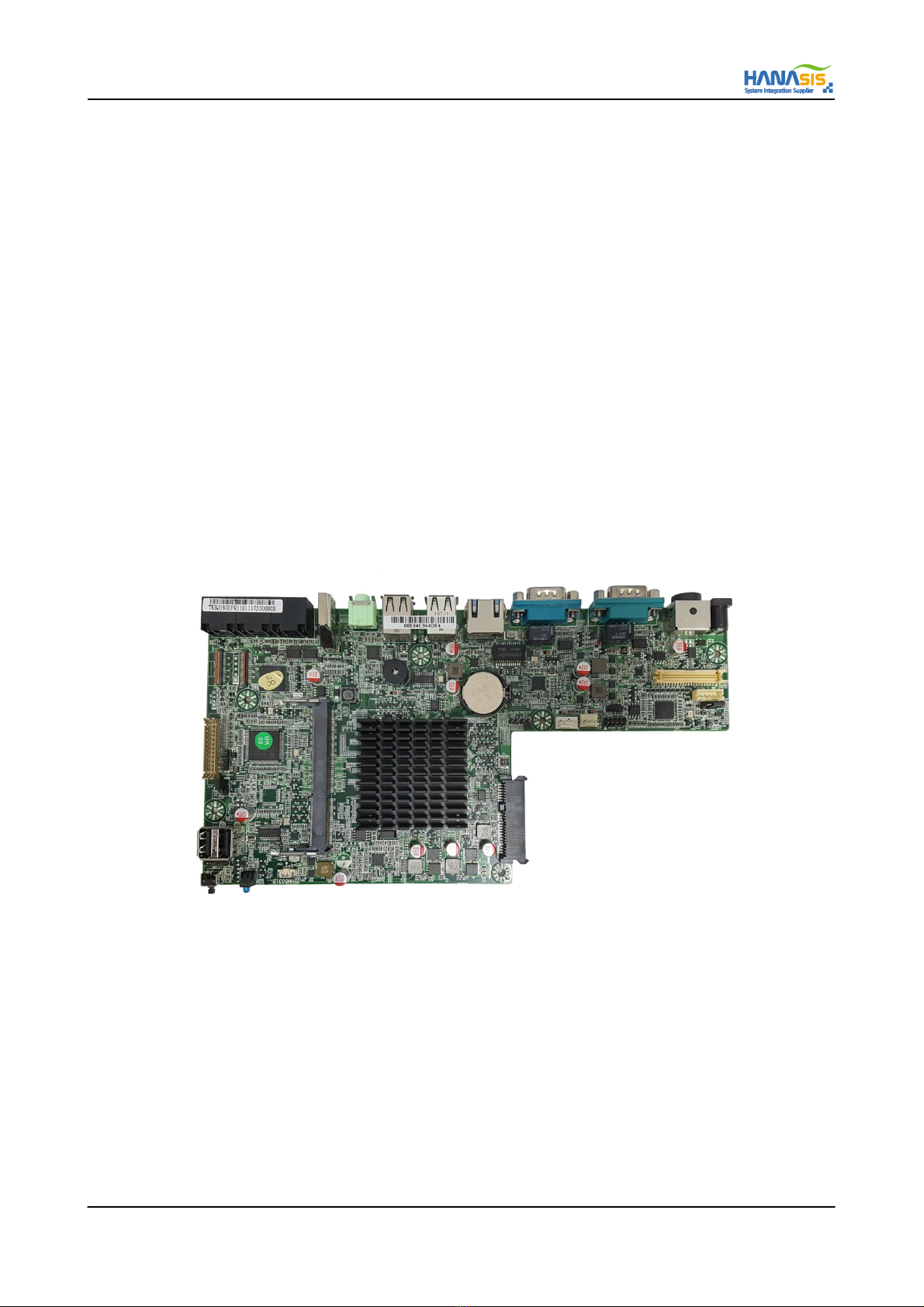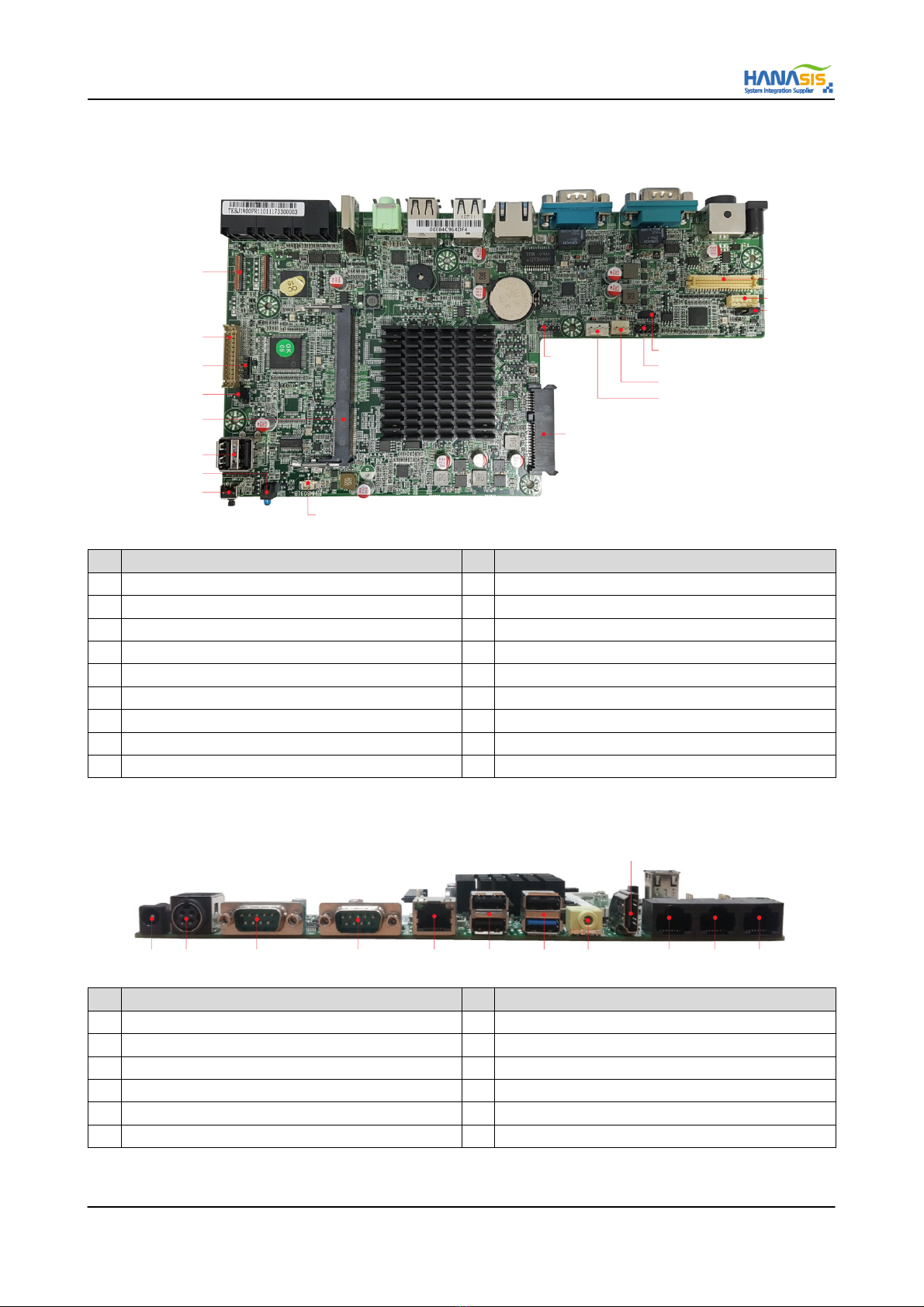
TEB-J1900A/P Mother Board Manual
2 / 26
Copyright Notice:
No part of this manual may be reproduced, transcribed, transmitted, or translated in any language, in any form or by any means,
except duplication of documentation by the purchaser for backup purpose, without written consent of Hanasis&Ruide.
Products and corporate names appearing in this manual may or may not be registered trademarks or copyrights of their respective
companies, and are used only for identification or explanation and to the owners’ benefit, without intent to infringe.
Disclaimer:
Specifications and information contained in this manual are furnished for informational use only and subject to change without
notice, and should not be constructed as a commitment by Hanasis&Ruide.
Hanasis&Ruide assumes no responsibility for any errors or omissions that may appear in this manual.
With respect to the contents of this manual, Hanasis&Ruide does not provide warranty of any kind, either expressed or implied,
including but not limited to the implied warranties or conditions of merchantability or fitness for a particular purpose.
In no event shall Hanasis&Ruide, its directors, officers, employees, or agents be liable for any indirect, special, incidental, or
consequential damages (including damages for loss of profits, loss of business, loss of data, interruption of business and the like),
even if Hanasis&Ruide has been advised of the possibility of such damages arising from any defect or error in the manual or
product.
This device complies with Part 15 of the FCC Rules. Operation is subject to the following two conditions:
(1) this device may not cause harmful interference, and
(2) this device must accept any interference received, including interference that may cause undesired operation.
CALIFORNIA, USA ONLY
The Lithium battery adopted on this motherboard contains Perchlorate, a toxic substance controlled in Perchlorate Best Management
Practices (BMP) regulations passed by the California Legislature. When you discard the Lithium battery in California, USA, please
follow the related regulations in advance.
“Perchlorate Material-special handling may apply, see www.dtsc.ca.gov/hazardouswaste/perchlorate”