Hitex ShieldBuddy TC275 User manual

User Manual
User Manual
4269.40100, 2.4, 2015-05
ShieldBuddy TC275 User Manual
Basic information on the ShieldBuddy TC275 development
board
Connectors, board layout, component placement, power options,
programming
Released

ShieldBuddy TC275 Development Platform
Aurix 32-Bit Triple Core
CONFIDENTIAL
Edition 2015-05
Published by:
Hitex (U.K.) Limited.
University Of Warwick Science Park, Coventry, CV4 7EZ, UK
© 2018 Hitex (U.K.) Limited.
All Rights Reserved.
Legal Disclaimer
The information given in this document shall in no event be regarded as a guarantee of conditions or
characteristics. With respect to any examples or hints given herein, any typical values stated herein and/or any
information regarding the application of the product, Hitex (UK) Ltd. hereby disclaims any and all warranties and
liabilities of any kind, including without limitation, warranties of non-infringement of intellectual property rights of
any third party.
Information
For further information on technology, delivery terms and conditions and prices, please contact the nearest
Hitex Office (www.hitex.co.uk).
ShieldBuddy TC275 Development Platform
Aurix 32-Bit Triple Core
CONFIDENTIAL
Released
3
2.4, 2015-05
Document Change History
Date
Version
Changed By
Change Description
8/8/2014
0.1
M Beach
First version
9/8/2014
0.2
M Beach
Revised top view
20/2/2015
0.3
M Beach/D Greenhill
Revised for Rev B HW
9/4/2015
0.8
M Beach
Added board test
16/9/2015
0.9
M Beach
Corrected P33.6
8/11/2016
1.0
M Beach
Added IDE extensions
29/11/2016
1.1
M Beach
Added new connector diagram
9/1/2017
1.2
M Beach
Changed Fast_digitalWrite()
13/1/2017
1.3
M Beach
Added Wire changes
23/1/2017
1.4
M Beach
Added EEPROM support.
13/2/2017
1.5
M Beach
Added improved SPI support (v1.30)
27/02/2017
1.6
M Beach
Added I2C channel on pins 16 and 17
7/3/2017
1.7
M Beach
Added new analogWrite and TriLib DSP
library
20/3/2017
1.8
M Beach
Added Ethernet bootloader
28/3/2017
1.9
M Beach
Added support for DC step TC275
24/4/2017
2.0
M Beach
Added Tone() functions. Updated CAN
8/5/2017
2.1
M Beach
Added PWM measurement functions
16/6/2017
2.2
M Beach
Corrected I2C pin naming for
SDA1/SCL1
24/7/2017
2.3
M Beach
Added inverted PWM measurement
06/10/2017
2.4
M Beach
Add Eclipse IDE debug setup
12/2/2018
2.5
M Beach
Updates for RevC hardware
We Listen to Your Comments
Is there any information in this document that you feel is wrong, unclear or missing?
Your feedback will help us to continuously improve the quality of this document.
Please send your comments (including a reference to this document) to:

ShieldBuddy TC275 Development Platform
Aurix 32-Bit Triple Core
CONFIDENTIAL
Released
4
2.4, 2015-05

ShieldBuddy TC275 Development Platform
Aurix 32-Bit Triple Core
CONFIDENTIAL
Released
5
2.4, 2015-05
Table of Contents
1Getting Started ...................................................................................................................................9
1.1 What Are The ShieldBuddy TC275 Tools?..........................................................................................9
1.2 Getting Started With The TC275 Toolchain.........................................................................................9
1.3 Using The ShieldBuddy TC275..........................................................................................................10
1.4 Using The Eclipse IDE .......................................................................................................................10
1.5 Debugging Programs Using Eclipse PLS UDE Debug Perspective ..................................................12
1.6 Getting Help .......................................................................................................................................16
2ShieldBuddy TC275 Extensions To The Arduino IDE .................................................................17
2.1 How is the ShieldBuddy Different To Other Arduinos?......................................................................17
2.2 TC275 Processor Architecture...........................................................................................................17
2.3 Serial Ports.........................................................................................................................................19
2.4 Multicore Programming Extensions ...................................................................................................19
2.4.1 Arduino IDE Extensions .....................................................................................................................19
2.4.2 Inter-Core Communications ...............................................................................................................20
2.4.2.1 Inter-Core Communications Example................................................................................................20
2.4.2.2 Using Interrupts To Coordinate and Communicate Between Cores..................................................22
2.4.3 Timers/Ticks/delay(), millis(), micros() Etc.........................................................................................23
2.4.3.1 Core 1.................................................................................................................................................24
2.4.3.2 Core 2.................................................................................................................................................24
2.4.3.3 Direct Fast Access To The System Timer0 .......................................................................................24
2.4.4 Managing the Multicore Memory Map................................................................................................25
2.5 Peripheral And IO Extensions............................................................................................................27
2.5.1 Faster digitalRead & digitalWrite........................................................................................................27
2.5.2 attachInterrupt() Function...................................................................................................................27
2.5.3 Enabling and Disabling Interrupts......................................................................................................27
2.5.4 ADC Read Resolution........................................................................................................................27
2.5.5 Fast ADC Conversions.......................................................................................................................28
2.5.6 analogWrite() & AnalogOut ................................................................................................................29
2.5.6.1 PWM Frequency.................................................................................................................................29
2.5.6.2 Custom PWM Frequencies ................................................................................................................29
2.5.6.3 Fast Update Of AnalogOut() Function ...............................................................................................29
2.5.6.4 DAC0 and DAC1 pins ........................................................................................................................29
2.6 CAN....................................................................................................................................................30
2.6.1 CAN Functions Usage........................................................................................................................30
2.6.1.1 Receiving any message regardless of message ID...........................................................................31
2.7 I2C/Wire Pins & Baudrate ..................................................................................................................32
2.8 EEPROM Support..............................................................................................................................33
2.9 Resetting The ShieldBuddy................................................................................................................33
2.10 SPI Support........................................................................................................................................33
2.10.1 Default Spi..........................................................................................................................................33
2.10.2 Spi Channel 1.....................................................................................................................................34
2.10.3 Spi Channel 2.....................................................................................................................................34
2.11 Aurix DSP Function Library................................................................................................................35
2.12 Ethernet BootLoader/In Application Ethernet Flash Programmer......................................................35
2.12.1 Overview ............................................................................................................................................35
2.12.2 Setting The Network Addresses.........................................................................................................35
2.12.3 Configuring The SPI...........................................................................................................................36
2.13 Using The Bootloader ........................................................................................................................36
2.14 Sending Programs To The ShieldBuddy............................................................................................37
2.15 Tone() Functions................................................................................................................................37
2.16 PWM Measurement Functions...........................................................................................................37
2.16.1 Using The PWM Measurement Functions .........................................................................................38
2.17 General Purpose Timer Interrupts......................................................................................................39
3Hardware Release Notes HW Revision B ......................................................................................40
3.1ShieldBuddy RevB Known Problems.................................................................................................40

ShieldBuddy TC275 Development Platform
Aurix 32-Bit Triple Core
CONFIDENTIAL
Released
6
2.4, 2015-05
3.2 CIC61508 (Safety version only).........................................................................................................40
3.3 VIN Pin...............................................................................................................................................40
4Arduino-Based Connector Details..................................................................................................41
4.1 Board Layout......................................................................................................................................41
4.2 Connector Pin Allocation....................................................................................................................42
4.3 TC275 ASCLIN to ShieldBuddy connector mapping .........................................................................44
5Powering The ShieldBuddy.............................................................................................................47
5.1Selectable Options.............................................................................................................................47
5.2 Restoring an ShieldBuddy with a completely erased FLASH............................................................47
6Underside Component Placement..................................................................................................48
7Appendices.......................................................................................................................................51
7.1 Basic Board Test................................................................................................................................51

ShieldBuddy TC275 Development Platform
Aurix 32-Bit Triple Core
CONFIDENTIAL
Released
7
2.4, 2015-05
List of Figures
Figure 1 TC275 Internal Layout........................................................................................................................17
Figure 2 TC275 Peripherals .............................................................................................................................18
Figure 3 TC275 RAMs......................................................................................................................................25
Figure 4 Top view of ShieldBuddy....................................................................................................................41
Figure 5 Extended IO Connector......................................................................................................................43
Figure 6 SPI Connector....................................................................................................................................43
Figure 7 TC275 to Arduino Connector Mapping ..............................................................................................46
Figure 8 TC275 to Arduino EXT IO Connector Mapping..................................................................................46
Figure 9 Bottom view of ShieldBuddy ..............................................................................................................48

ShieldBuddy TC275 Development Platform
Aurix 32-Bit Triple Core
CONFIDENTIAL
Released
8
2.4, 2015-05
List of Tables
Table 1 SPI Names.........................................................................................................................................34
Table 2 Pins available for tone() function........................................................................................................37
Table 3 Pins available for PWM measurement functions ...............................................................................37
Table 4 ASCLIN to ShieldBuddy connector mapping .....................................................................................44
Table 5 Arduino To ShieldBuddy To TC275 Mapping ....................................................................................44

ShieldBuddy TC275 Development Platform
Aurix 32-Bit Triple Core
CONFIDENTIAL
Released
9
2.4, 2015-05
1 Getting Started
1.1 What Are The ShieldBuddy TC275 Tools?
The main ShieldBuddy toolchain is the Eclipse-based “FreeEntryToolchain” from Hightec/PLS/ Infineon. This is
a full C/C++ development environment with source-level debugger. The familiar Arduino IDE is also available
for the ShieldBuddy. Both IDEs are based on the Infineon iLLD libraries and allow the usual Arduino C++- like
Processing language to be used with the familiar Arduino IO funcitions e.g. digitalWrite(), analogRead(),
Serial.print() etc.. These functions are implemented for all three TC275 cores and can be used without
restriction.
Given the awesome power of the TC275 we expect most users to program it in C in Eclipse, using the iLLD API
directly or working with the underlying SFRs. The neat thing about the ShieldBuddy is that it lets you access the
massive power of the TC275 without knowing anything about the bits and bytes of the peripherals!
1.2 Getting Started With The TC275 Toolchain
If you have never used an Arduino-style board before then
is a good idea to have a look at www.arduino.cc to find out
what it is all about! Although the ShieldBuddy contains
three powerful 32-bit, 200MHz processors, it can be used
in exactly the same way as an ordinary Arduino Uno. The
same Arduino IDE can be used but with an add-on to
allow triple core operation. To use the ShieldBuddy you
will need:
(i) a PC with Windows Vista or later
(ii) The Aurix free toolchain with Eclipse, C/C++ compiler
and UDE debugger from PLS:
http://free-entry-toolchain.hightec-rt.com/
Follow the instructions given as you will need a free
licence file which will be automatically emailed to you.
You will need to copy it to : C:\HIGHTEC\licenses.
(iii) The standard 1.8.0 Arduino IDE installed from:
http://arduino.cc/download.php?f=/arduino-1.8.0-
windows.exe
Make sure you install this in the default directory!
If you do not have admin rights on your PC then use this
version:
https://downloads.arduino.cc/arduino-1.8.0-windows.zip
ShieldBuddy TC275 Development Platform
Aurix 32-Bit Triple Core
CONFIDENTIAL
Released
10
2.4, 2015-05
(iv) The Arduino development environment add-in for Eclipse and the standard Arduino IDE:
http://www.hitex.co.uk/fileadmin/uk-files/downloads/ShieldBuddy/ShieldBuddyMulticoreIDE.zip
Unzip this to a temporary directory using the zip password “ShieldBuddy”. Run the installer and use the
password “ShieldBuddy” to copy the IDE onto your PC.
Install these in the order Aurix freetoolchain, Arduino IDE, ShieldBuddy IDE. We hope to combine these into a
single installer in the near future to make the installation quicker.
1.3 Using The ShieldBuddy TC275
Once all of the above packages have been installed, use the ShieldBuddy just like any other Arduino except that
you have three processors to play with rather than just one. Processor core 0 will run setup() and loop() with
processor cores 1 and 2 running setup1()/setup2() and loop1()/loop2(). There are no special measures required
to write triple-core programs but make sure that that you do not try to use the same peripheral with two different
cores at the same time. Whilst nothing nasty will happen, your programs will probably just not work properly!
Each core is basically identical except that cores 1 and 2 are about 20% faster than core 0, having an extra
pipeline stage. They all can use the same Arduino Processing language functions. When choosing which
ShieldBuddy to use in the Arduino IDE, if you have a board with a CA-step processor (SAK-TC275TP-64
F200W CA EES A), choose “ShieldBuddy TC275”. If you have a DC-step board (SAK-TC275TP-64 F200N
DC), choose “ShieldBuddy TC275_Dx”.
Remember to press the reset button on the ShieldBuddy to make it run the new program.
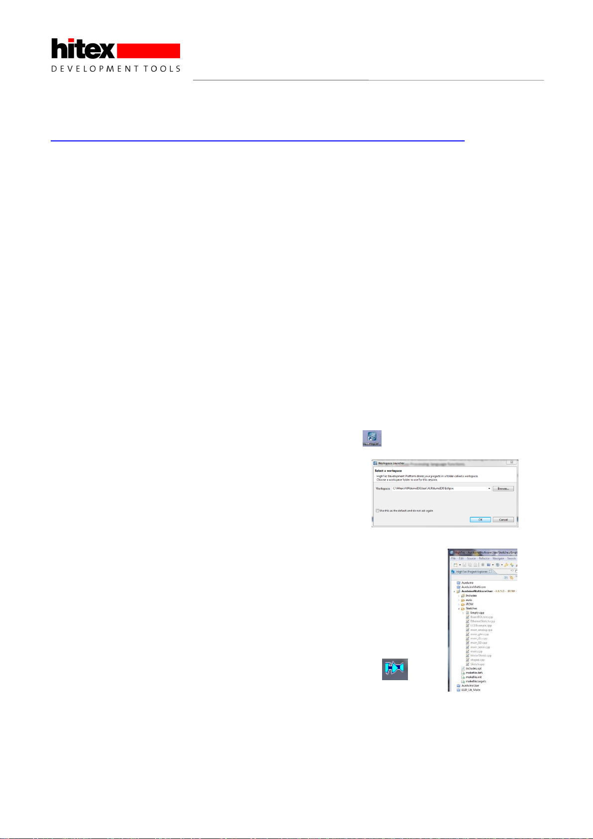
1.4 Using The Eclipse IDE
If you want to use the Eclipse environment, start the toolchain with the icon. When prompted, open the
workspace at:
C:\Hitex\AURDuinoIDE\Eclipse
The default project is AURduinoMulticoreUser:
Arduino-style sketches are stored in the Sketches directory. The default sketch
“Empty.cpp” is a simple program that uses all three cores. You can overwrite the
statements we used with your own.
To get your programs into the ShieldBuddy, use the PLS UDE debugger
Open the workspace (ShieldBuddy with TC275 DC step processor):
“C:\Hitex\AURduinoIDE\Eclipse\AurduinoMulticoreUser\.ude\ShieldBuddyWorkspace_27xD.wsx”
Or (ShieldBuddy with TC275 CA step processor) :
“C:\Hitex\AURduinoIDE\Eclipse\AurduinoMulticoreUser\.ude\ShieldBuddyWorkspace_27xC.wsx”

ShieldBuddy TC275 Development Platform
Aurix 32-Bit Triple Core
CONFIDENTIAL
Released
11
2.4, 2015-05
The program will automatically load. You can run it by clicking the icon and stop it with the icon. To
reset the program, use the icon. You can find more information on using the Eclipse tools and the PLS UDE
debugger in the guide supplied with the FreeToolChain.

ShieldBuddy TC275 Development Platform
Aurix 32-Bit Triple Core
CONFIDENTIAL
Released
12
2.4, 2015-05
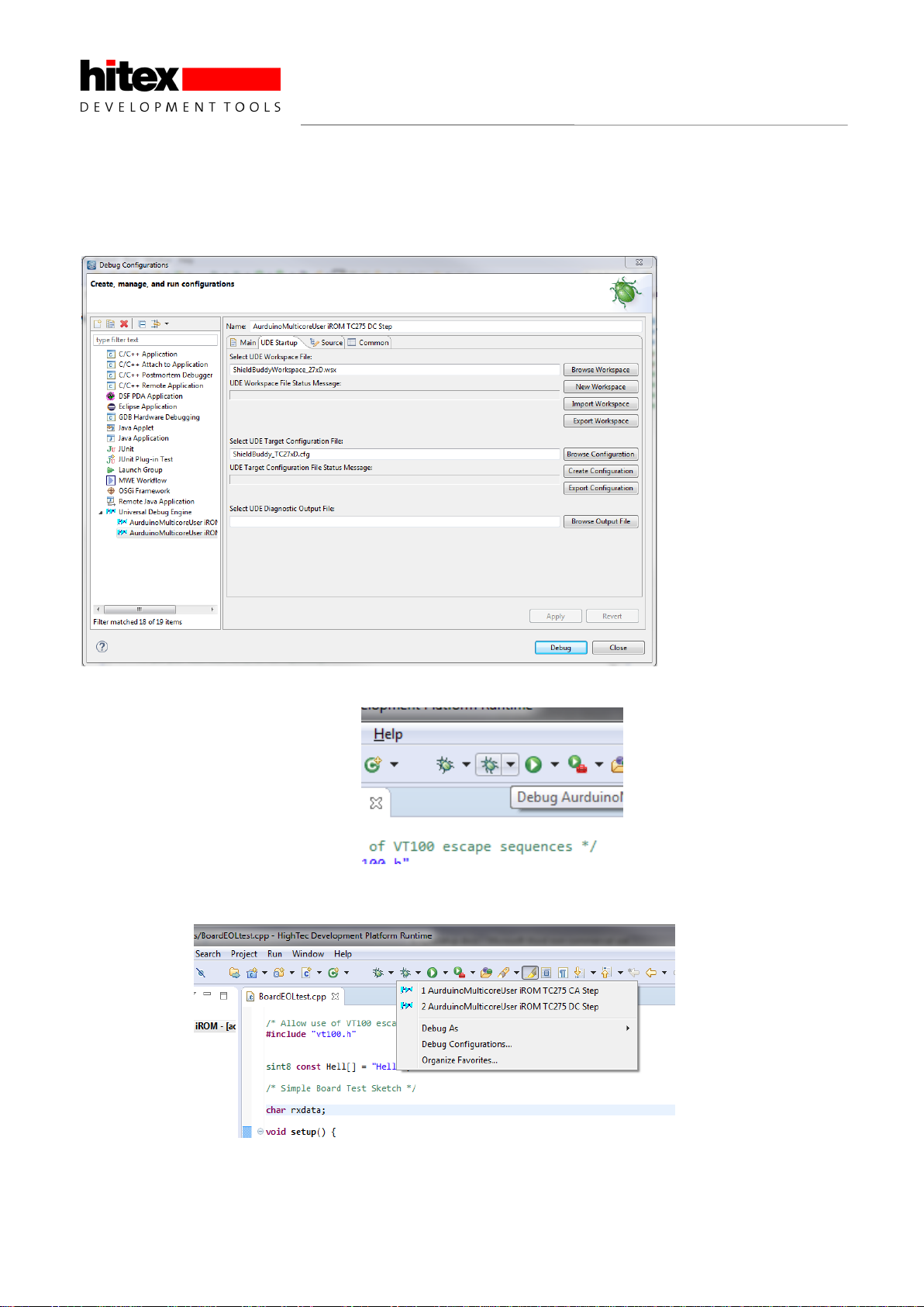
1.5 Debugging Programs Using Eclipse PLS UDE Debug Perspective
Unfortunately some configuring is required to use the UDE perspective for debugging under Eclipse. This is
performed as follows. Please note that this will depend on whether you have a TC275 CA or DC step on your
ShieldBuddy.
Create a new Debug Target to suit your Aurix version. Here we will do the TC275 DC first.
Then create a new debug configuration with …

ShieldBuddy TC275 Development Platform
Aurix 32-Bit Triple Core
CONFIDENTIAL
Released
13
2.4, 2015-05
Here we are setting up for the TC275 DC step. The C/C++ Application will be as shown –you will need to
browse for this.
ShieldBuddy TC275 Development Platform
Aurix 32-Bit Triple Core
CONFIDENTIAL
Released
14
2.4, 2015-05
Under the “UDE Startup” tab, you need to specify the UDE workspace file to use. This is predefined in
“C:\Hitex\AURduinoIDE\Eclipse\AurduinoMulticoreUser\.ude”. The Target Configuration file is predefined in
C:\Hitex\AURduinoIDE\Eclipse\AurduinoMulticoreUser\.ude\.target”. You will need to browse for both of these
files.
Now click the Apply button. You can run the debugger directly from here using “Debug”…
…or you can do it from the Debug icon in Eclipse.

ShieldBuddy TC275 Development Platform
Aurix 32-Bit Triple Core
CONFIDENTIAL
Released
15
2.4, 2015-05
The UDE debug perspective should now open…
If you are using a TC275 CA step board then you need to define a debug configuration for this in the same way
as we did for the DC step.
Create a new Debug Target …

ShieldBuddy TC275 Development Platform
Aurix 32-Bit Triple Core
CONFIDENTIAL
Released
16
2.4, 2015-05
Then create a new debug configuration with …
Now click the Apply button. You can run the debugger directly from here using “Debug”…
…or you can do it from the Debug icon in Eclipse.
You can now use the UDE debug perspective in the usual; Eclipse manner!
1.6 Getting Help
If you need help, there is a new on-line forum at http://ShieldBuddy.boards.net/.
This hardware user manual with the pinouts is at http://www.hitex.co.uk/index.php?id=3650.

ShieldBuddy TC275 Development Platform
Aurix 32-Bit Triple Core
CONFIDENTIAL
Released
17
2.4, 2015-05
2 ShieldBuddy TC275 Extensions To The Arduino IDE
2.1 How is the ShieldBuddy Different To Other Arduinos?
Most Arduino-style boards use AVR or ARM/Cortex processors which are fine for basic messing about with
micros - these chips are everywhere in consumer gadgets and devices. The ShieldBuddy is different, having
the mighty Infineon Aurix TC275 processor. These are normally only to be found in state of the art engine
management systems, ABS systems and industrial motor drives in your favourite German automobile. They
rarely make it out into the daylight of the normal hobbyist/maker world and to date have only been known to a
select few at Bosch, BMW, Audi, Daimler-Benz etc..
The standard Arduino IDE can be used, provided that the ShieldBuddy add-in has been installed. Programs
can be written in exactly the same way as on an ordinary Arduino. However to make best use of the multicore
TC275 processor, there are some special macros and functions available.
2.2 TC275 Processor Architecture
Unlike the AVR, SAM3 etc. used on normal Arduinos, the TC275 has three near-identical 200MHz 32-bit CPU
cores on a shared bus, each with their own local RAM but sharing a common FLASH ROM. The peripherals
(timers, port pins, Ethernet, serial ports etc.) are also shared, with each core having full access to any
peripheral.
Figure 1 TC275 Internal Layout
FPU
System Peripheral Bus (SPB)
Abbreviations:
PFlash: Program Flash
DFlash: Data Flash (EEPROM)
: SRI Slave Interface
: SRI Master Interface
TC1.6E
CPU0
Lockstep
PMI
DMI
24 KB Code
RAM 112 KB RAM
XBAR
PMU0
SRI Cross Bar Interconnect (XBar_SRI)
FPU
OCDS
L1 Debug
Interface/JTAG
DMA
64 channels
M
M/S
M
M/S M/S
FPU
TC1.6P
CPU1
Lockstep
PMI
DMI
32 KB Code
RAM 120 KB RAM
FPU
M/S M/S
DFlash
384 KB
PFlash0
2 MB PFlash1
2 MB
S S S
S
M
32 KB
RAM
S
LMU
FPU
TC1.6P
CPU2
PMI
DMI
32 KB Code
RAM 120 KB RAM
FPU
M/S M/S
M M
System Peripheral Bus (SPB)
Bridge
(SFI)
S
M
SRI Cross Bar Interconnect (XBar_SRI)
To The Peripherals

ShieldBuddy TC275 Development Platform
Aurix 32-Bit Triple Core
CONFIDENTIAL
Released
18
2.4, 2015-05
The TC275 CPU core design has a basic 5ns cycle time which means you can get typically around 150 to 200
32-bit instructions per microsecond. This is seriously fast when you consider that the Arduino Uno’s
Atmega328P only manages around sixteen 8-bit instructions/us! In addition, there is a floating point unit on
each core so using floating point variables does not slow things down significantly.
Figure 2 TC275 Peripherals
With so much computing horsepower available, the TC275 can manage a huge range of peripherals. Besides
commonplace peripherals like CAN, ADC, I2C, Ethernet, SPI etc. the TC275 has possibly the most powerful
signal measurement and generation block to be found on any microcontroller (GTM) plus a an advanced super-
fast delta-sigma analog to digital converter.
The Generic Timer Module (GTM) is the main source of pulse generation and measurement functions
containing over 200 IO channels. It is designed primarily for automotive powertrain control and electric motor
drives. Unlike conventional timer blocks, time-processing units, CAPCOM units etc. it can work in both the time
and angle domains without restriction. This is particularly useful for mechanical control systems, switch-
reluctance motor commutation, crankshaft synchronisation etc.
Under the bonnet the GTM has around 3000 SFRs but fortunately you do not need to know any of these to
realize useful functions! It is enormously powerful and the culmination of 25 years of meeting the needs of high-
end automotive control systems. However it can and indeed has been successfully applied to more general
industrial applications, particularly in the field of motor control where is can drive up to 4 three-phase motors.
The Arduino analogWrite() function makes use of it in a simple way to generate PWM. It can also flash a LED.
There is a second timer block (GPT12) can be used for encoder interfaces. Usefully most port pins can
generate direct interrupts.
With 176 pins required to get these peripherals out and only 100 pins on the Arduino Due form factor, some
functions have had to be limited. The 32 ADC channels have been limited to 12 and the 48 potential PWM
channels are also limited to 12, although more channels can be found on the double row expansion connector, if
needed.
FlexRay
(2 Channels)
System Peripheral Bus (SPB)
ASC + LIN
MultiCAN+
(4 Nodes, 256 MO)
CAPCOM0
( CCU60, CCU61)
BCU
Ports
QSPI 4
GTM
Timer Block
FCE
MSC 2
STM
Sytem Timers
4SENT
(10 Channels)
48 + 12
6*2
(x=0-5)
DS-ADCx
(x=0-7)
VADCx
EtherMAC
GPT12
3
IOM
48 + 12
PSI5-S
Interrupt
Router
PSI5
(3 Channels)
I2C
To the CPU cores & memory

ShieldBuddy TC275 Development Platform
Aurix 32-Bit Triple Core
CONFIDENTIAL
Released
19
2.4, 2015-05
2.3 Serial Ports
The Arduino has the Serial class for sending data to the UART which ultimately ends up as a COM port on the
host PC. The ShieldBuddy has 4 potential hardware serial ports so there are now 4 Serial classes. The default
Serial class that is directed to the Arduino IDE Serial Monitor tool becomes SerialASC on the ShieldBuddy.
Thus Serial.begin(9600) becomes SerialASC.begin(9600) and Serial.print(“Hi”) becomes SerialASC.print(“Hi”)
and so on.
The serial channels are allocated as per:
SerialASC Arduino FDTI USB-COM micro USB
Serial1 RX1/TX1 Arduino J403 pins 17/16
Serial0 RX0/TX0 Arduino J403 pins 15/14
Serial RX/TX Arduino default J402 pins D0/D1
Any of the serial channels can be used from any core but it is not a good idea to access the same serial port
from more than one core at the same time –see the later section on multicore programming.
2.4 Multicore Programming Extensions
2.4.1 Arduino IDE Extensions
The standard Arduino IDE has been extended to allow the
all 3 cores to be used. Anybody used to the default
Arduino sketch might notice though that in addition to the
familiar setup() and loop(), there is now a setup1(), loop1()
and setup2(), loop2(). These new functions are for CPU
cores 1 and 2 respectively. So while Core0 can be used
as on any ordinary Arduino, the lucky programmer can now
run three applications simultaneously.
Core0 can be regarded as the master core in the context of
the Arduino as it has to launch the other two cores and
then do all the initialisation of the Arduino IO, timer tick (for
millis() and micros() and delay()). Thus setup1() and
setup2() are reached before setup()!
Although all three cores are notionally the same, in fact
cores1 and 2 are about 25% faster than core0 as they
have an extra pipeline stage. Thus it is usually best to put
any heavyweight number crunching tasks on these cores.
Writing for a multicore processor can be a bit mind-bending
at first! The first thing to realise is that there is only one
ROM and the Arduino IDE just compiles source code. It
has no idea (and does not need to know) which core a
particular function will run on. It is only when the program
runs that this becomes fixed. Any function called from
setup and loop() will run on core0; any called from setup1()
and loop1() will execute on core1 and so on. Thus is
perfectly possible for the same function you wrote to
execute simultaneously on all three cores. As there is only
one image of this function in the FLASH, the internal bus
structure of the Aurix allows all three cores to access the same instructions at the same addresses (worst case)
at exactly the same time. Note that if this extreme case happens, there will be a slight loss of performance.
Sharing of functions between cores is easy, provided that they do not make use of the peripherals! Whilst there
are three cores, there are only two ADCs. If all three cores want to access the same result register, there is no
particular problem with this. However if you want a timer to generate an interrupt and call a shared function,

ShieldBuddy TC275 Development Platform
Aurix 32-Bit Triple Core
CONFIDENTIAL
Released
20
2.4, 2015-05
then that function might need to know which core it is currently running on! This is easy to do as there is a
macro defined to return the core number.
if(GetCpuCoreID() == 2)
{
/* We must be running on core 2! */
}
Fortunately it is rare to have to do this but it is used extensively in the ShieldBuddy to Arduino translation layer.
2.4.2 Inter-Core Communications
One of the aims of the AURIX multicore design is to avoid the awkward programming issues that can arise in
multicore processors and make the system architect’s job easier. The three independent cores exist within a
single memory space (0x00000000 –0xFFFFFFFF), so they are all able to access any address without
restriction. This includes all the peripherals and importantly all FLASH and RAM areas.
Having a consistent global address space when accessing RAM can considerably ease the passing of data
between cores using shared structures. Supporting high performance when doing this is achieved by the
implementation of a crossbar bus system to connect the cores, memories and DMA systems. Of course there
are protection mechanisms that can generate traps for such accesses if the application requires it, as they may
indicate a program malfunction which would need to be handled in an orderly manner.
The upshot of this is that the programmer does not need to worry about cores accessing the same memory
location (i.e. variable) at the same time. In some multicore processors this would cause an exception and is
regarded as an error. Certainly if you are new to multicore programming, this makes life much easier. Of
course there could be a contention at the lowest level and this can result in extra cycles being inserted but given
the speed of the CPU, this is unlikely to be an issue with Arduino-style applications.
With an application split across three cores, the immediate problem is how to synchronise operations. As the
Aurix design allows RAM locations to be accessed by any core at any time, this is no problem. In the simplest
case, global variables can be used to allow one core to send a signal to another. Here is an example.
2.4.2.1 Inter-Core Communications Example
We want to use the SerialASC.print() function to allow each core to send a message to the Arduino Serial
Monitor –something like “Hello From Core 0”, “Hello From Core 1” etc..
If we do nothing clever and just allow each core’s Loop() to write to the SerialASC, we get a complete jumble of
characters. This is because each core will write to the transmit buffer at random times. The Aurix does not care
that 3 cores are trying to use the same serial port and nothing nasty like an exception will happen. All the
characters are in there from all the cores but not necessarily in the right order.
What we need to do is make sure that each core waits in turn for the other cores to finish writing to the serial
port. This is quite easy using some global variables. However with true multicore programming, weird things
can happen that don’t occur in single core.
Table of contents
Other Hitex Motherboard manuals


