Holtek HT66FV1 0 Series Instruction Manual

HT66FV1x0 Integrated Audio Amplifier Application Guideline
AN0486EN V1.10 1 / 16 June 8, 2021
HT66FV1x0 Integrated Audio Amplifier
Application Guideline
D/N: AN0486EN
Introduction
The Holtek HT66FV1x0 series of MCUs include a 16-bit DAC for digital volume control, a class
AB audio power amplifier, SPI and UART interfaces, etc., making them applicable for use in a wide
range of home appliances, health care products, security protection and many other consumer
electronic products that require an audio function. As these MCUs contain an internal 1.5W high
power audio amplifier together with digital volume control functions, they can cater to customers’
demand for high quality sound without requiring an external power amplifier. With the advantages
of simplified external component requirements and competitive overall costs, the devices should
find excellent use in a wide range of voice playing products.
This text will take the HT66FV1x0 series as an example to introduce the operating principles,
features and usage of the MCU integrated audio power amplifier.
Functional Description
A power amplifier is the most basic device in an audio system. Power amplifiers can amplify a
weak input signal from a sound source or a pre-amplifier and then generate a current large enough
to drive the speaker for voice playing. Some common amplifier types are Class A, Class B, Class
AB and Class D.
Class A Principles
Class A is the simplest type. In a Class A amplifier, the output transistor remains in a conducting
state over the entire range of input signal cycle, i.e., the conduction angle is 360 degrees. As Class
A amplifiers operate within the linear portion of their individual characteristic curve, they have less
transient distortion and crossover distortion problems, however with low efficiency. The quiescent
operating point of the amplifier is near the midpoint of the load line. A load characteristic curve
directly reflects the relation between the load voltage and current change. The intersection of the
load line and the transistor output characteristic curve is the quiescent operating point, which is
used to analyse the circuit quiescent point and distortion situations.

HT66FV1x0 Integrated Audio Amplifier Application Guideline
AN0486EN V1.10 2 / 16 June 8, 2021
IC
IC IC
t
Load Line
Output
Waveform
Quiescent Point
Vi Input Waveform
Quiescent
Point
V
BE
V
CE
Class A
Class B Principles
The quiescent operating point of a Class B amplifier is located on the output characteristic curve
with a base current of zero, namely the cut-off point of the load line. In a Class B amplifier, a single
output transistor conducts only one half of the input signal cycle, that is, the conduction angle is
180 degrees. To amplify a complete signal, two transistors are used, one for the positive output
signal and the other for the negative output signal. A pseudo load, RL, is connected to the amplifier
output port, replacing the normal power receiving component, which is used to debug the power
amplifier circuit. After the debug has been successfully completed, a true load, a speaker is
connected. The efficiency of Class B amplifiers is much improved over Class A amplifiers.
However, at the crossover point from the on to off state of the two transistors, the distortion of Class
B is higher.
IC
IC
IC
t
t
Output
Waveform
Load Line
Quiescent
Point
Quiescet
Point
Vi Input Waveform Crossover
Distortion
V
BE
V
CE
Class B
Class AB Principles
The Class AB design contains the advantages of both Class A and Class B. The quiescent operating
point of Class AB amplifier, which is lower than Class A but higher than Class B, is located between
the load line midpoint and cut-off point, resulting in efficiencies higher than Class A and distortion
lower than Class B. The conduction angle is in the range of 180~360 degrees. By biasing the two
transistors, when the signal is close to zero, both transistors are turned on with a relatively small
current, which is similar to Class A. In the case of a large signal, when one of the transistors turns
off the other must turn on. The two transistors are always turned on alternatively, which is similar
to Class B. The crossover distortion of Class B amplifiers is caused by the fact that neither transistor
can conduct when the input signal is in the range of -0.6V~0.6V. In a Class AB amplifier, a VBB
bias is applied between the two transistors to reduce the crossover distortion.
Q1
V+
Q1
RL
V+
V-
Q2

HT66FV1x0 Integrated Audio Amplifier Application Guideline
AN0486EN V1.10 3 / 16 June 8, 2021
IC IC
Class B
Crossover Distortion
Class AB Crossover
Distortion Eliminated
Q2 On
Q1 On Q1 On
Vbe Vbe
Class AB
Class D Principles
Class D amplifiers operate based on an MOS transistor on/off switching. Transistors can be
completely switched on or off in a very short time providing a relatively high efficiency. However,
this switching mode of operation adds distortion to the output signals. The Class D modulator is a
PWM modulator composed of a comparator and a triangle wave generator. The input signal is
filtered by an integrator to generate a corrected signal, which is used to modulate the triangle wave
to produce the modulated square wave output. A MOSFET driver is used for high power voltage
and current amplification after which the amplified digital signal is filtered by a low-pass filter to
restore the analog audio signal.
Class D
Modulator
MOSEFET
Driver
Low-pass Filter
Class D
Advantages and Disadvantages Comparison – Class AB Amplifiers vs. Other
Power Amplifiers
For Class AB, its efficiency is higher than Class A and its distortion is lower than Class B. The
operating mode of Class D is totally different from Class AB. In a Class D amplifier, some high
frequency harmonics will be generated therefore EMI will be greater. Class AB amplifiers have a
significant cost advantage over Class D amplifiers, because the latter are usually two or three times
the price of the former. In general, Class AB amplifiers have the advantages of higher efficiency, lower
distortion and lower costs, which make them the most widely used design in audio amplifier
applications at present.
Q1
RL
V+
V-
Q2

HT66FV1x0 Integrated Audio Amplifier Application Guideline
AN0486EN V1.10 4 / 16 June 8, 2021
The advantages and disadvantages of the aforementioned amplifier types are summarised in the table
below.
Class A
Class B
Class AB
Class D
Operating Point
Location
Load line midpoint Load line cut-off point
Between load line midpoint
and cut-off point
Transistors operate in a
switching mode
Conduction Angle
θ=360°
θ=180°
180°<θ<360°
Switching status
Distortion
Lower distortion
Higher than Class AB with
crossover distortion
Crossover distortion can be
eliminated
Higher distortion
Power Transfer
Efficiency
Lowest efficiency, under
50%
Efficiency in the rage of
50%~78.5%
Efficiency in the rage of
50%~78.5%
Highest efficiency,
higher than 85%
Main Application
s Low power amplifiers
with small distortion High power amplifiers General audio speakers High power or high
efficiency amplifiers
Amplifier Electrical Characteristics
The characteristics of the HT66FV1x0 integrated Class AB amplifier is listed in the following table
(Ta=25°C).
Total Harmonic Distortion – THD
When a sinusoidal signal of a particular frequency is input to the power amplifier, harmonics based
on input frequency multiples are generated due to factors such as the amplifier internal circuit or
external component non-linear distortion. The ratio between the root mean square value of these
harmonic amplitudes and the input frequency amplitude is called the total harmonic distortion.
Noise – N
In addition to the harmonic distortion described above, there might be other interference caused by
circuit and components, such as thermal noise, etc.
The total harmonic distortion and noise are combined to describe the output noise index, which
should be as small as possible. The typical value of (THD+N)/S can be as low as 0.2% for the
HTFV1x0 series.
Maximum Output Power – POUT
This character reflects the output capacity of an audio power amplifier. Usually the audio amplifier
manufacturer will provide several product POUT values for certain operating voltages and rated load
conditions. The output power of the MCU integrated power amplifier is 1.5W when VDD is 5V and
(THD+N)/S equals 10%.
Users should select a proper speaker according to the amplifier output power and impedance. The
speaker power is usually a little higher than the amplifier power. It is suggested that the speaker
impedance should match the corresponding load parameters listed below.

HT66FV1x0 Integrated Audio Amplifier Application Guideline
AN0486EN V1.10 5 / 16 June 8, 2021
Symbol Parameter
Test Condition
Min. Typ. Max. Unit
V
DD
Condition
AV
DD_PA
Audio Power Amplifier
Operating Voltage – – 2.2 – 5.5 V
(THD+N)/S
(THD+N)/S 5V 8Ω load,
Output power=500mW – 0.2 – %
P
OUT Output Power
3V
8Ω load, (THD+N)/S=1%
–
410
–
mW
8Ω load, (THD+N)/S=10%
–
550
–
mW
5V
8Ω load, (THD+N)/S=1%
–
1200
–
mW
8Ω load, (THD+N)/S=10% – 1500 – mW
Note: Sine wave input @1kHz & -6dB.
Operating Principles
The HT66FV1x0 includes an integrated Class AB high output power audio amplifier, which will
be introduced in this section. Using its integrated SPI interface the HT66FV1x0 reads digital audio
data from the external Flash ROM and writes it into the 16-bit DAC data registers PLADH and
PLADL. Each piece of data will be converted into a corresponding audio analog voltage signal by
the DAC after which the speaker will play the corresponding sound.
The HT66FV1x0 voice playing function block diagram is shown as follows. DAEN and PAEN are
the DAC and amplifier enable bits respectively, which can be cleared to zero to reduce power
consumption when the voice playing function is not used. The USVC[6:0] field is used for digital
volume adjustment.
PLADH
PLADL
USV C[6:0]
16-bit D/A +
PowerAmplifier
ker
Voice Playing Controller Registers
The overall voice playing function of the HT66FV1x0 is controlled using a series of registers. Two
control registers exist to control the 16-bit D/A converter and power amplifier functions together
with the speaker mute control. Two data registers exist to store the data which is to be played.
USVC Register
Bit
7
6
5
4
3
2
1
0
Name
MUTEB
USVC6
USVC5
USVC4
USVC3
USVC2
USVC1
USVC0
R/W
R/W
R/W
R/W
R/W
R/W
R/W
R/W
R/W
POR 0 0 0 0 0 0 0 0
Bit7 MUTEB: Speaker mute control
0: Mute speaker output
1: Enable speaker output
Bit6~0 USVC6~USVC0: Speaker volume control
These bits are used to control the volume which ranges from -32dB to 6dB.

HT66FV1x0 Integrated Audio Amplifier Application Guideline
AN0486EN V1.10 6 / 16 June 8, 2021
PLAC Register
Bit
7
6
5
4
3
2
1
0
Name
–
–
–
–
–
–
PAEN
DAEN
R/W – – – – – – R/W R/W
POR
–
–
–
–
–
–
0
0
Bit7~2 Unimplemented, read as “0”
Bit1 PAEN: Power amplifier enable control
0: Disable
1: Enable
Bit0 DAEN: 16-bit D/A converter enable control
0: Disable
1: Enable
Note that the 16-bit D/A converter and power amplifier will all be disabled when the MCU enters
the IDLE/SLEEP mode.
PLADL Register
Bit
7
6
5
4
3
2
1
0
Name
P_D7
P_D6
P_D5
P_D4
P_D3
P_D2
P_D1
P_D0
R/W
R/W
R/W
R/W
R/W
R/W
R/W
R/W
R/W
POR
0
0
0
0
0
0
0
0
Bit7~0 P_D7~P_D0: Paly data low byte register bit7~bit0
This register is used to store the 16-bit play data low byte.
PLADH Register
Bit
7
6
5
4
3
2
1
0
Name
P_D15
P_D14
P_D13
P_D12
P_D11
P_D10
P_D9
P_D8
R/W R/W R/W R/W R/W R/W R/W R/W R/W
POR
0
0
0
0
0
0
0
0
Bit7~0 P_D15~P_D8: Paly data high byte register bit7~bit0
This register is used to store the 16-bit play data high byte. Note that the low byte play data register
should first be modified followed by the high byte play data register being written if the 16-bit play
data is necessary to be updated.

HT66FV1x0 Integrated Audio Amplifier Application Guideline
AN0486EN V1.10 7 / 16 June 8, 2021
Hardware Description
The HT66FV1x0 MCU includes an integrated voice playing controller and voice data stored in an
external SPI Flash ROM can be read via the integrated SPI interface. This makes voice content
changes more convenient. A complete 5V application circuit is shown below.
AVDD_PA is connected to the VCC power and AVSS_PA is the power amplifier ground pin. SP+
and SP- are externally connected to a speaker. AUD is the DAC output pin and AUD_IN is the
power amplifier input pin. The audio signal output on the AUD pin will first be filtered by a low-
pass RC filter and then input to the AUD_IN pin via capacitive coupling. Whether to connect a
variable resistor to AUD/AUD_IN is optional according to the desired volume control method. A
10µF capacitor is connected to the BIAS pin for bias reference voltage stabilisation and filtering.
Pin
Description
SP+
Power amplifier output positive end
SP-
Power amplifier output negative end
AUD_IN
Power amplifier input
BIAS
Power amplifier internal reference voltage
AUD
16-bit DAC output
AVDD_PA
Power amplifier positive power supply
AVSS_PA
Power amplifier negative power supply
PCB Layout Considerations
When placing components, priority should be given to the power supply filter capacitors which
should be located as close to the MCU as possible. This is also the case for the SPI Flash ROM
and especially the SPI clock line which should be as short as possible.
To avoid noise interference caused by instantaneous large currents during audio amplifier
operations, two separate power supplies are required, VDD for digital power and AVDD_PA
for analog power.

HT66FV1x0 Integrated Audio Amplifier Application Guideline
AN0486EN V1.10 8 / 16 June 8, 2021
The audio amplifier power pin AVDD_PA should be wired directly to the positive power supply
and the line width should not be less than 12mil.
To avoid noise interference caused by instantaneous large currents during audio amplifier
operations, two separate grounds are required, VSS for digital ground and AVSS_PA for analog
ground.
The audio amplifier ground pin AVSS_PA should be wired directly to the negative power
supply and the line width should not be less than 12mil.
The VSS and AVSS_PA are two separate grounds and should be implemented with copper
layers.
Ensure that enough space is reserved for the power and ground lines when placing components.
The power amplifier outputs, SP+/SP-, tracks should be thick and free of through holes.
As right angles tend to accumulate charge resulting in point discharge effects, which can
influence the PCB stability, it is better to route tracks using 45-degree angles or arc angles.
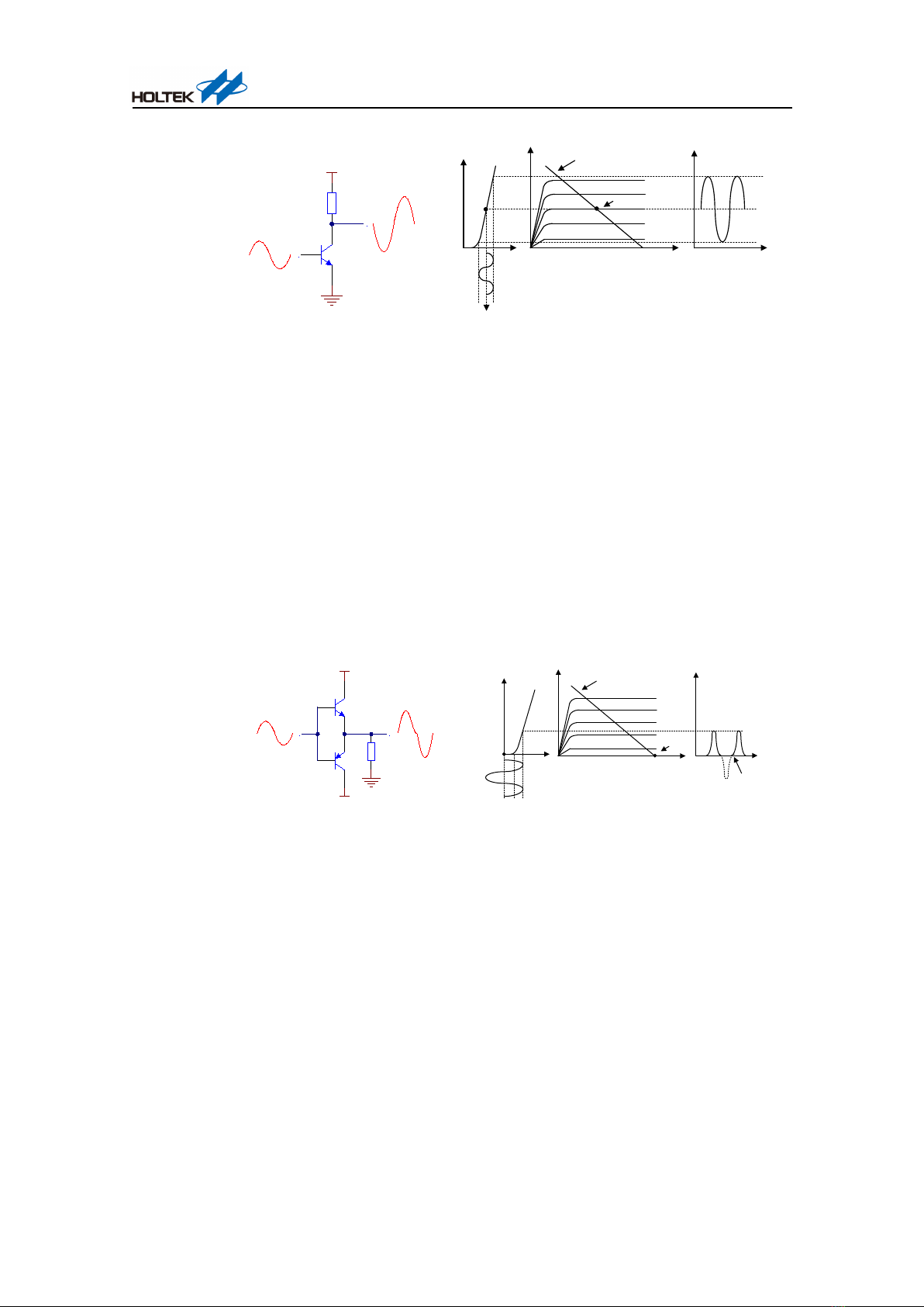
Software Description
Voice Playing Controller Setup
The HT66FV1x0 controls the voice playing function using several registers, as described below.
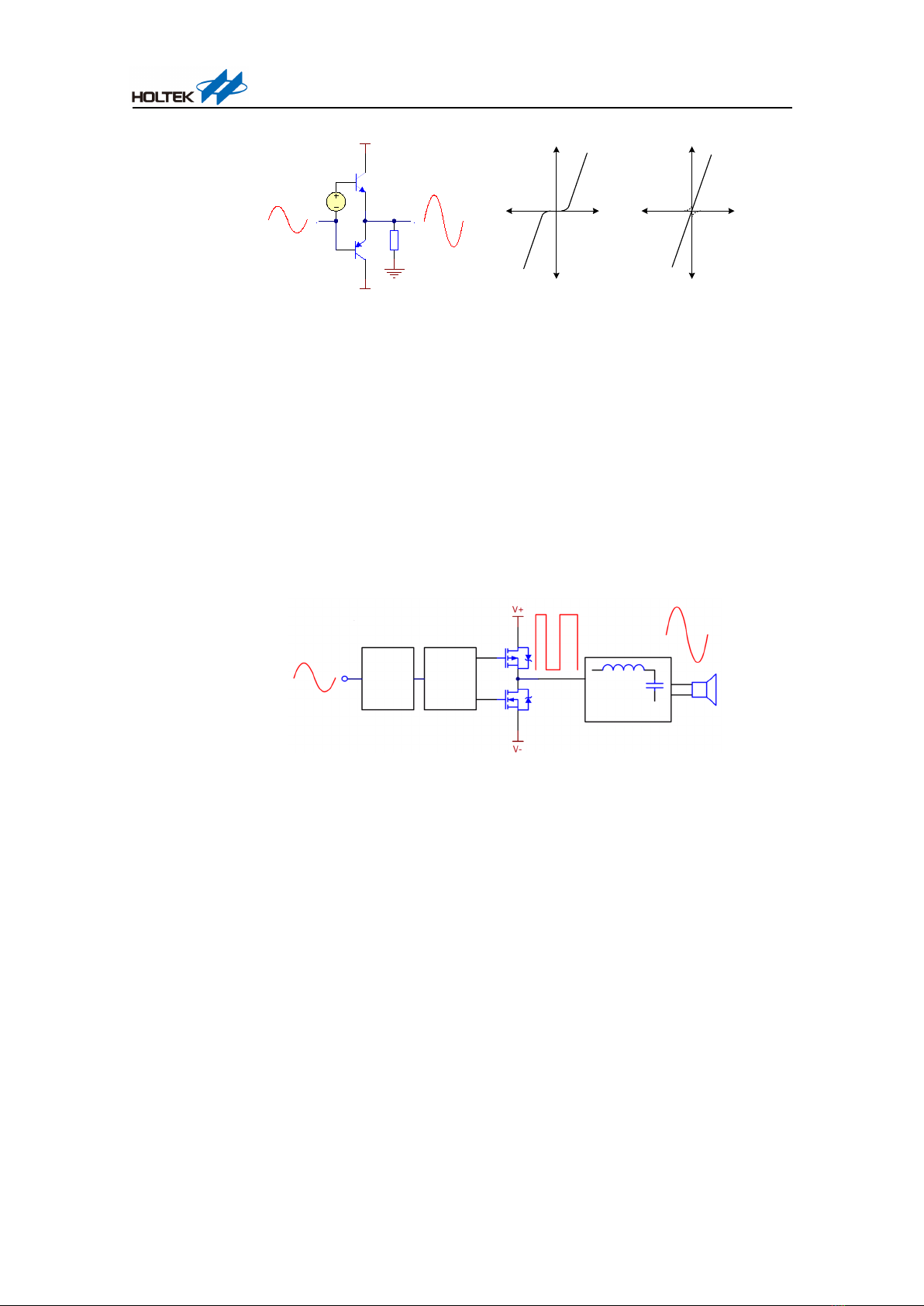
1. When the PAEN (PLAC.1) bit is set high, the power amplifier is enabled. When the DAEN
(PLAC.0) bit is set high, the 16-bit D/A converter is enabled.
2. When the MUTEB (USVC.7) bit is set high, the speaker is enabled.
3. There are two methods for volume control.
Analog volume control: Externally connect a variable resistor between the DAC output pin,
AUD, and the power amplifier analog input pin, AUD_IN. The DAC output signal is first
attenuated via the resistor divider and then input to the power amplifier. This method is
suitable for applications which use a rotary knob to adjust volume.
Digital volume control: Use the USVC6~USVC0 software bits to control the speaker
volume. This can be used to adjust the speaker volume within a range of +6dB to -32dB.
Each stage is 0.5dB for high volume applications or 1dB for low volume applications.
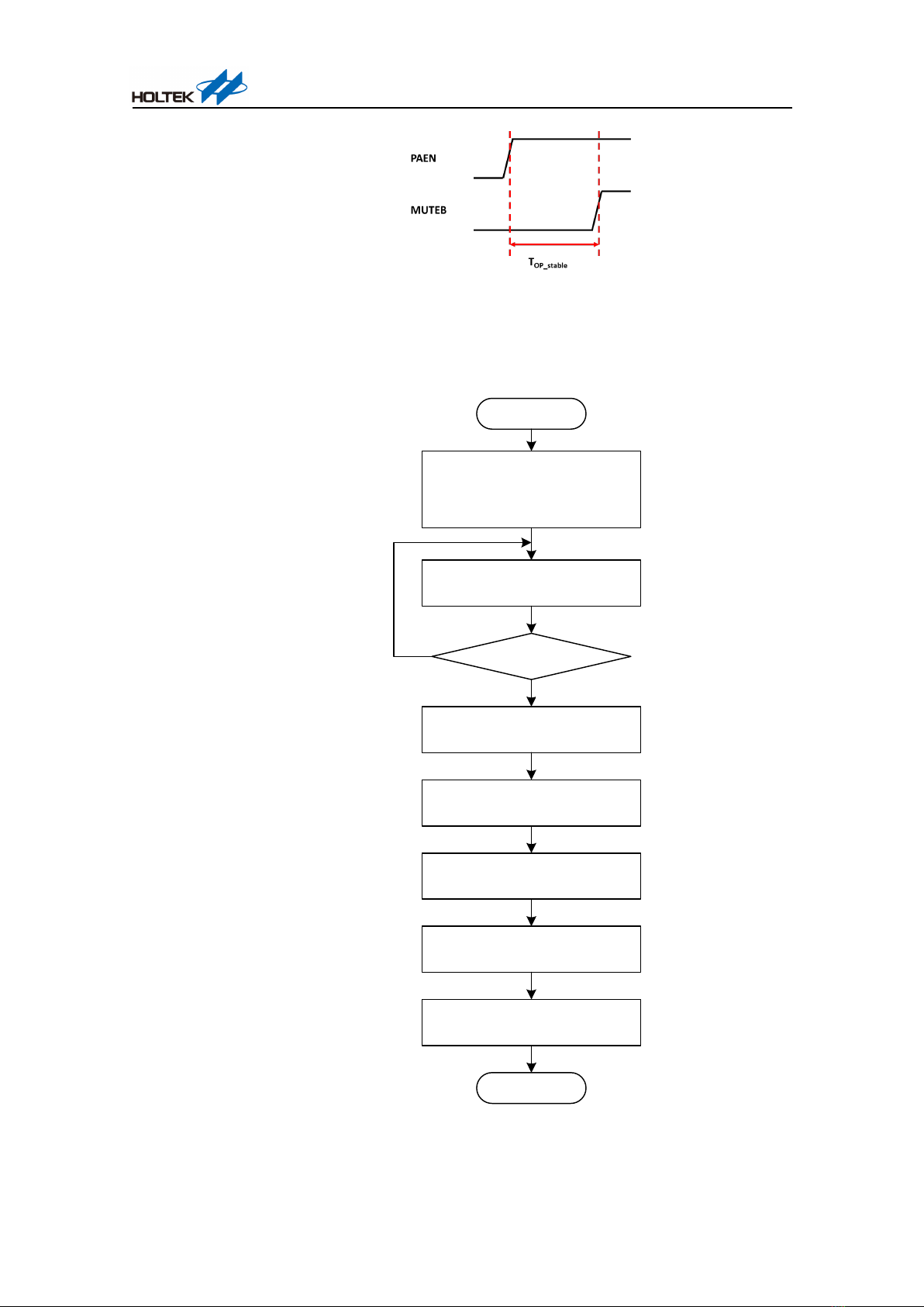
4. Voice data is stored in the external SPI Flash ROM. The MCU reads voice data from the SPI
Flash using its integrated SPI interface.
5. Each 16-bit section of voice data is placed in the PLADL and PLADH registers. Use a timer to
generate interrupt signals at regular intervals, read the voice data from the SPI Flash each time
an interrupt is generated and write it into the 16-bit DAC. After this the analog signal amplified
by the integrated power amplifier will be output to drive the speaker to produce sound.

HT66FV1x0 Integrated Audio Amplifier Application Guideline
AN0486EN V1.10 9 / 16 June 8, 2021
Power On/Off Pop Noise
Pop noise is produced by the transient impact of various operations at the moment of power on or
power off of audio devices. To suppress pop noise, pay special attention to the following processes.
Process of Starting Voice Playing
(1) Power On Sequence
Power On
SPI On
(pin PC7/SCSAB→1)
Ramp Up
Ready
SPI On
Enable VDDIO
PBS0[1:0]→11B
Enable SPI Pin
PCS1→0x55
set SAMLS, SACSEN
SPIAC0→0x00
SPIAC1→0x0C
set SPIAEN
SPIAEN→1
Return
When starting to read the Flash, setting the PC7/SCSAB pin from 1 to 0 will cause V33 to
change instantaneously, which will affect VCC resulting in unstable output. To solve this
problem, set the PC7/SCSAB pin from 1 to 0 and then initiate the ramp up process. This will
ensure a stable power supply when playing voices with reduced pop noise.
(2) Ramp Up
When powering on, charge the output pins (SP+/SP-) gradually to a level of 1/2 VDD, wait for
a certain time until the power amplifier has a stable output, then output voice to the speaker. By
following this sequence, pop noise can be effectively suppressed. The specific settings are
summarised below.
Initial status: (PLADH/PLADL)=0000H, DAEN=1, PAEN=0, MUTEB=1,
USVC6~USVC0=000_0000
Increase the value of PLADH/PLADL gradually from 0000H to 8000H
Volume setup: USVC6~USVC0 =target value
MUTEB=0
Enable the power amplifier (PAEN=1), wait for a certain time until it has a stable output
Enable the speaker (MUTEB=1) for voice playing

HT66FV1x0 Integrated Audio Amplifier Application Guideline
AN0486EN V1.10 10 / 16 June 8, 2021
Note: Generally speaking, the time shown in the figure should be greater than 200ms to
effectively suppress pop noise. A longer time will ensure a better suppression effect. This
time varies with different speakers.
Ramp up software flow as shown below
Ramp Up
Voice Playing Register Initialisation
(PLADL=0 ; PLADH=0 ; DAE N=1 ;
PAEN=0 ; MUTEB=1 ;
USVC6~USVC0=000_0000)
16-bit Play Data (PLADH/PLADL)+1
PLADH/PLADL=8000H?
Volume Setup
(USVC6~USVC0 = Target Value)
Mute Speaker Output
(MUTEB=0)
Enable Power Amp lifier Output
(PAEN=1)
Delay 200ms*
Enable Speaker Output
(MUTEB=1)
Return
Y
N
*: This time is not fixed but should be adjusted according to the actual condition.

HT66FV1x0 Integrated Audio Amplifier Application Guideline
AN0486EN V1.10 11 / 16 June 8, 2021
Process of Stopping Voice Playing
(1) Ramp Down
When powering off:
Disable the power amplifier (PAEN=0)
Increase PLADH/PLADL gradually to 8000H
Volume setup: USVC6~USVC0=000_0000
Decrease PLADH/PLADL gradually from 8000H to 0000H
Disable the DAC and speaker (DAEN=0, MUTEB=0)
Ramp down software flow as shown below
Ramp Down
Disable Power Amplifier
(PAEN=0)
PLADH/PLADL=8000H? PLADH/PLADL>8000H? 16-bit Play Data
(PLADH/PLADL)+1
16-bit Play Data
(PLADH/PLADL)-1
Volume Setup
(US VC6~USVC0=000_0000)
16-bit Play Data
(PLADH/PLADL)-1
PLADH/PLADL=0000H?
Disable Speaker and DAC
(MUT EB=0, DAEN=0)
Return
Y
Y
NN
Y
N
(2) Power Off Sequence
Similar to the power on sequence, setting the PC7/SCSAB pin from 0 to 1 will cause
instantaneous change of V33, which will affect VCC resulting in unstable output. Initiate the
ramp down process first when the SPI is still on (PC7/SCSAB=0) before setting the pin from 0
to 1 to disable the SPI function. This will reduce pop noise.

HT66FV1x0 Integrated Audio Amplifier Application Guideline
AN0486EN V1.10 12 / 16 June 8, 2021
Power Off
Ramp Down
SPI Off
(pin PC7/SCSAB→0)
Off
SPI Off
clear SPIAEN
SPIAEN→0
clear SAMLS, SACSEN
SPIAC1→0x00
Disable SPI Pin
PCS1→0x00
Disable VDDIO
PBS0[1:0]→00B
Return
The following provides the demo codes for the ramp up and ramp down software flows, which aim
to avoid pop noise when switching on/off the DAC and audio power amplifier. Demo code settings
are as follows (fSYS=8MHz).
(1) Power On Sequence settings using ASM language
MAIN_START:
CALL SPI_ON
CALL RAMP_UP
(2) SPI On settings using ASM language
SPI_ON:
; enable VDDIO
MOV A,PBS0
OR A,03H
MOV PBS0,A
; enable SPI pins
MOV A,01010101B
MOV PCS1,A
; set SAMLS, SACSEN
CLR SPIAC0
MOV A, 0CH
MOV SPIAC1, A
; set SPIAEN
SET SPIAEN
RET
(3) Ramp Up settings using ASM language
RAMPUP:
MOV A,00H
MOV PLADL,A ; initialise DAC 16-bit data
MOV PLADH,A
SET DAEN ; enable 16-bit D/A converter
CLR PAEN ; disable power amplifier
MOV A,80H ; MUTEB=1 to enable speaker; volume=000_0000
MOV USVC, A
LOOP1:

HT66FV1x0 Integrated Audio Amplifier Application Guideline
AN0486EN V1.10 13 / 16 June 8, 2021
CALL DELAY_10US
MOV A,1 ; increase PLADH/PLADL from 0000H to 8000H
ADDM A,PLADL
MOV A,0
ADCM A,PLADH
SNZ PLADH.7
JMP LOOP1
MOV A,00H ; volume = target value, MUTEB=0 to disable speaker
MOV USVC, A
SET PAEN ; enable power amplifier
CALL DELAY_200MS ; wait before power amplifier is stable
SET MUTEB ; MUTEB=1 to enable speaker
RET
(4) Power On Sequence settings using V3 C language
SPI_ON();
RAMP_UP();
(5) SPI On settings using V3 C language
void SPI_ON(void)
{
_pbs0 = _pbs0 | 0x03; // enable VDDIO
_pcs1 = 0x55; // enable SPI pins
// set SAMLS, SACSEN
_spiac0 = 0x00;
_spiac1 = 0x0C;
_spiaen = 1; // set SPIAEN
}
(6) Ramp Up settings using V3 C language
void RAMP_UP(void)
{
unsigned int j;
_pladl = 0x00; // initialise DAC 16-bit data
_pladh = 0x00;
_daen = 1; // enable 16-bit D/A converter
_paen = 0; // disable power amplifier
_usvc = 0x80; // MUTEB=1 to enable speaker; volume=000_0000
PLAD = 0x0000;
while(PLAD != 0x8000) // increase PLADH/PLADL from 0000H to 8000H
{
GCC_CLRWDT();
GCC_DELAY(10);
PLAD+=1;
_pladl = PLAD;
_pladh = PLAD >>8;
}
_usvc = 0x00; // volume = target value, MUTEB=0 to disable speaker
_plac = 0x03; // enable power amplifier
for(j= 0;j<300;j++) // wait before power amplifier is stable
{
GCC_CLRWDT();
GCC_DELAY(4000);
}
_usvc = 0x80; // MUTEB=1 to enable speaker
}
(7) Ramp Down settings using ASM language
RAMPDOWN:
CLR PAEN ; disable power amplifier
COMPARE_EQUAL: ; increase PLADH/PLADL gradually to 8000H
MOV A,PLADH
XOR A,80h

HT66FV1x0 Integrated Audio Amplifier Application Guideline
AN0486EN V1.10 14 / 16 June 8, 2021
SNZ Z
JMP COMPARE_LARGER
MOV A,PLADL
XOR A,00h
SNZ Z
JMP COMPARE_LARGER
JMP VOICE_OFF
COMPARE_LARGER:
CALL DELAY_10US
SZ PLADH.7
JMP DECREASE ; jump if PLAD>8000H
JMP INCREASE ; jump if PLAD<8000H
DECREASE:
MOV A,0FFH
ADDM A,PLADL
MOV A,0FFH
ADCM A,PLADH
JMP COMPARE_EQUAL
RET
INCREASE:
MOV A,1
ADDM A,PLADL
MOV A,0
ADCM A,PLADH
JMP COMPARE_EQUAL
VOICE_OFF:
MOV A,80H ; volume=000_0000
MOV USVC, A
LOOP2:
CALL DELAY_10US
MOV A,0FFH ; decrease PLADH/PLADL from 8000H to 0000H
ADDM A,PLADL
MOV A,0FFH
ADCM A,PLADH
SZ PLADL
JMP LOOP2
SZ PLADH
JMP LOOP2
CLR MUTEB ; disable speaker output
CLR DAEN ; disable 16-bit D/A converter
RET
(8) Power Off Sequence settings using ASM language
MAIN_START:
CALL RAMP_DOWN
CALL SPI_OFF
(9) SPI Off settings using ASM language
SPI_OFF:
CLR SPIAEN ; clear SPIAEN
CLR SPIAC1 ; clear SAMLS, SACSEN
CLR PCS1 ; disable SPI pin
MOV A,PBS0 ; disable VDDIO
AND A,0FCH
MOV PBS0,A
RET
(10) Ramp Down settings using V3 C language
void RAMP_DOWN(void)
{
_paen=0; // disable power amplifier
PLAD =((unsigned int)_pladh<<8) | _pladl;
while(PLAD != 0x8000) // increase PLADH/PLADL gradually to 8000H

HT66FV1x0 Integrated Audio Amplifier Application Guideline
AN0486EN V1.10 15 / 16 June 8, 2021
{
GCC_CLRWDT();
GCC_DELAY(10);
if(PLAD > 0x8000)
{
PLAD--;
_pladl = PLAD;
_pladh = PLAD >>8;
}
else
{
PLAD++;
_pladl = PLAD;
_pladh = PLAD >>8;
}
}
_usvc = 0x80; // volume=000_0000
while(PLAD) // decrease PLADH/PLAD from 8000H to 0000H
{
GCC_CLRWDT();
GCC_DELAY(10);
PLAD-=1;
_pladl = PLAD;
_pladh = PLAD >>8;
}
_usvc = 0x00; // disable speaker output
_daen = 0; // disable 16-bit D/A converter
}
(11) Power Off Sequence settings using V3 C language
RAMP_DOWN();
SPI_OFF();
(12) SPI Off settings using V3 C language
void SPI_OFF(void)
{
_spiaen = 0x00; // clear SPIAEN
_spiac1 = 0x00; // clear SAMLS, SACSEN
_pcs1 = 0x00; // disable SPI pin
_pbs0 = _pbs0 & 0xFC; // disable VDDIO
}
Conclusion
By using this HT66FV1x0 series integrated audio power amplifier functional introduction, users should
have a better understanding of the Holtek 8-bit MCU integrated power amplifier function application.
Versions and Modification Information
Date
Author
Version
Modification
2021.3.12
李玉梅
V1.10
Solve the problem of insufficient pop noise processing
2018.4.30
藍愛娣
V1.00
First version

HT66FV1x0 Integrated Audio Amplifier Application Guideline
AN0486EN V1.10 16 / 16 June 8, 2021
Reference File
Reference file: HT66FV130/140/150/160 datasheet.
For more information refer to the Holtek’s official website www.holtek.com.
Disclaimer
All information, trademarks, logos, graphics, videos, audio clips, links and other items appearing
on this website ('Information') are for reference only and is subject to change at any time without
prior notice and at the discretion of Holtek Semiconductor Inc. and its related companies
(hereinafter 'Holtek', 'the company', 'us', 'we' or 'our'). Whilst Holtek endeavors to ensure the
accuracy of the Information on this website, no express or implied warranty is given by Holtek to
the accuracy of the Information. Holtek will bear no responsibility for any incorrectness or leakage.
Holtek will not be liable for any damages (including but not limited to computer virus, system
problems or data loss) whatsoever arising in using or in connection with the use of this website by
any party. There may be links in this area, which allow you to visit the websites of other companies.
These websites are not controlled by Holtek. Holtek will bear no responsibility and no guarantee to
whatsoever Information displayed at such sites. Hyperlinks to other websites are at your own risk.
Limitation of Liability
In any case, the Company has no need to take responsibility for any loss or damage caused when
anyone visits the website directly or indirectly and uses the contents, information or service on the
website.
Governing Law
This disclaimer is subjected to the laws of the Republic of China and under the jurisdiction of the
Court of the Republic of China.
Update of Disclaimer
Holtek reserves the right to update the Disclaimer at any time with or without prior notice, all
changes are effective immediately upon posting to the website.
Table of contents