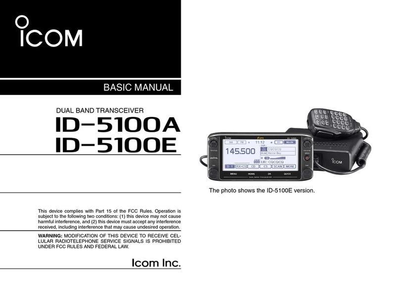
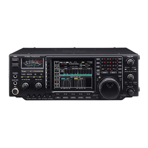
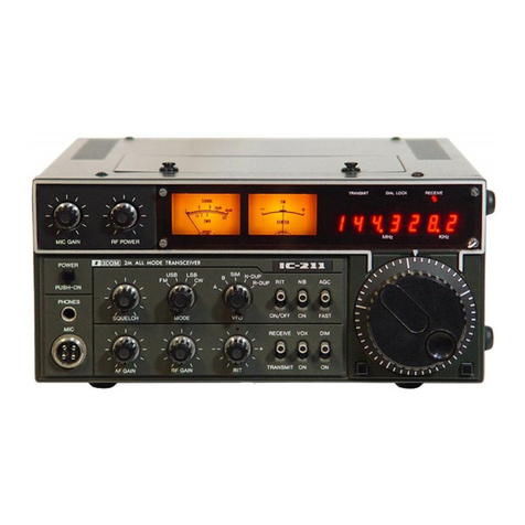
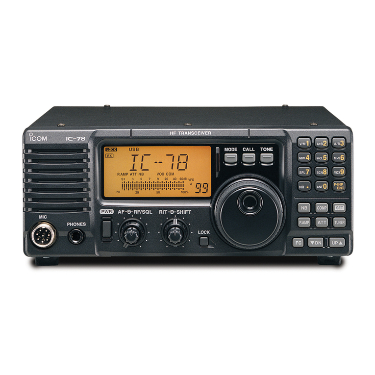
Icom IC-7851 Building instructions

S-15119XZ-C1
March 2015
THE TRANSCEIVER

This service manual describes the latest technical informa-
tion for the IC-7850/IC-7851 THE TRANSCEIVER, at the time of
publication.
ONLY connect the transceiver to an AC outlet that is
85 to 265 V.
DO NOT expose the transceiver to rain, snow or liquids.
DO NOT apply an RF signal of more than 20 dBm (100 mW) to
the antenna connector. This could damage the transceiver’s
front-end.
To upgrade quality, any electrical or mechanical parts
and internal circuits are subject to change without notice
or obligation.
MODEL VERSION VERSION
NUMBER
IC-7851
USA [#02]
EUR [#03]
FRA [#04]
UK [#05]
ITR [#06]
ESP [#07]
KOR [#08]
IC-7850 USA-01 [#22]
EUR-01 [#23]
Be sure to include the following four points when ordering
replacement parts:
1. 10-digit Icom part number
2. Component name
3. Equipment model name and unit name
4. Quantity required
<ORDER EXAMPLE>
1110003491 S.IC TA31136FNG IC-7851 MAIN UNIT 5 pieces
8820001210 Screw 2438 screw IC-7851 Top cover 10 pieces
Addresses are provided on the inside back cover for your
convenience.
ORDERING PARTS
1. Make sure that the problem is internal before dis-assem-
bling the transceiver.
2. DO NOT open the transceiver until the transceiver is dis-
connected from its power source.
3. DO NOT force any of the variable components. Turn them
slowly and smoothly.
4. DO NOT short any circuits or electronic parts. An insulated
tuning tool MUST be used for all adjustments.
5. DO NOT keep power ON for a long time when the trans-
ceiver is defective.
6. DO NOT transmit power into a Standard Signal Generator
or a Sweep Generator, otherwise the RF power may dam-
age them.
7. ALWAYS connect a 50 dB to 60 dB attenuator between the
transceiver and a Deviation Meter or Spectrum Analyzer,
when using such test equipment.
8. READ the instructions of the test equipment thoroughly
before connecting it to the transceiver.
REPAIR NOTES
INTRODUCTION CAUTION
(IC-7851)
Icom, Icom Inc. and the Icom logo are registered trademarks of Icom Incorporated (Japan) in Japan, the United States, the
United Kingdom, Germany, France, Spain, Russia, and/or other countries.

TABLE OF CONTENTS
SECTION 1 SPECIFICATIONS
SECTION 2 INSIDE VIEWS
SECTION 3 ADJUSTMENT PROCEDURES
3-1 PREPARATION ................................................................................................... 3-1
3-2 FINAL AND DRIVER IDLING CURRENT ADJUSTMENTS................................ 3-5
3-3 PRESET ADJUSTMENTS .................................................................................. 3-7
3-4 REF ADJUSTMENTS ......................................................................................... 3-8
3-5 ID ADJUSTMENTS............................................................................................. 3-9
3-6 TX ADJUSTMENTS ............................................................................................ 3-10
3-7 RX ADJUSTMENTS ........................................................................................... 3-14
3-8 SCOPE ADJUSTMENT ...................................................................................... 3-21
3-9 TUNER ADJUSTMENT....................................................................................... 3-21
SECTION 4 PARTS LIST
SECTION 5 MECHANICAL PARTS
SECTION 6 BOARD LAYOUTS
SECTION 7 BLOCK DIAGRAM
SECTION 8 VOLTAGE DIAGRAM

1-1
SECTION 1
.
SPECIFICATIONS
■Specifications
DGeneral
• Frequency coverage (unit: MHz):
Receiver 0.030000–60.000000*1
Transmitter 0.135700–0.137800*2, 1.800000–1.999999*2,
3.500000–3.999999*2, 5.255000 – 5.405000*1, *2,
7.000000–7.300000*2, 10.100000–10.150000*2,
14.000000–14.350000*2, 18.068000–18.168000*2,
21.000000–21.450000*2, 24.890000–24.990000*2,
28.000000–29.700000*2, 50.000000–54.000000*2
*1Some frequency ranges are not guaranteed.
*2Depending on versions.
• Operating mode: USB/LSB (J3E), CW (A1A), RTTY (F1B), PSK31/63
(G1B), AM (A3E), FM (F3E)
• Number of memory channels:101 (99 regular, 2 scan edges)
• Antenna connectors:SO-2394 (antenna impedance: 50 Ω)
• Operating temperature range: 0˚C to +50˚C, +32˚F to +122˚F
• Frequency stability:Less than ±0.05 ppm (approximately 5 minutes after turning ON
the main power, [I/O], ON, 0–50˚C (32–122˚F), 54.000000 MHz)
• Frequency resolution: 1 Hz (minimum)
• Power supply requirement: 85–265 V AC (universal input)
• Power consumption:
Power OFF Standby 15 VA typical (at 100 V AC)
Remote Standby 20 VA typical (at 100 V AC)
Receive Standby 150 VA typical
Maximum audio 150 VA typical
Transmit at 200 W 800 VA
• Dimensions (projections not included): 425 (W)×149 (H)×435 (D) mm, 16.7 (W)×5.9 (H)×17.1 (D) in
• Weight: Approximately 23.5 kg, 52 lb
• ACC 1 connectors: 8-pin DIN connector2
• ACC 2 connectors: 7-pin DIN connector2
• EXT-DISPLAY connector: DVI-I
• CI-V connector: 2-conductor 3.5 (d) mm (1⁄8)
• KEYBOARD connector: USB-A
DTransmitter
• Transmit output power:
SSB, CW, RTTY, PSK, FM Less than 5–200 W
AM Less than 5–50 W
137 kHz band More than –20 dBm (Europe version only)
• Modulation system:
SSB P.S.N. modulation
AM Low power modulation
FM Phase modulation
• Spurious emission:
Harmonics More than 60 dB (HF bands)
More than 70 dB (50 MHz band)
Spurious (except harmonics) More than 50 dB (HF bands)
More than 70 dB (50 MHz band)
Out of band emission More than 40 dB (HF bands)
More than 60 dB (50 MHz band)
• Carrier suppression: More than 63 dB
• Unwanted side-band suppression: More than 70 dB
• ∂TX variable range: ±9.999 kHz
• Microphone connector: 8-pin connector (600 Ω)
• ELEC-KEY connector: 3-conductor 6.35 (d) mm (1⁄4)
• KEY connector: 3-conductor 6.35 (d) mm (1⁄4)
• RELAY connector: Phono (RCA)
• ALC connector: Phono (RCA)
1-2
DReceiver
• Receive system: Double conversion superheterodyne system
• Intermediate frequencies:
1st 64.455 MHz (MAIN band)
64.555 MHz (SUB band)
2nd 36 kHz
• Sensitivity:
SSB, CW, RTTY, PSK (BW=2.4 kHz, 10 dB S/N)
0.100–1.799 MHz 0.5 µV (pre-amp 1 ON)
1.800–29.990 MHz 0.16 µV (pre-amp 1 ON)
50.000–54.000 MHz 0.13 µV (pre-amp 2 ON)
AM (BW=6 kHz, 10 dB S/N)
0.100–1.799 MHz 6.3 µV (pre-amp 1 ON)
1.800–29.990 MHz 2 µV (pre-amp 1 ON)
50.000–54.000 MHz 1 µV (pre-amp 2 ON)
FM (BW=15 kHz, 12 dB SINAD)
28.000–29.990 MHz 0.5 µV (pre-amp 1 ON)
50.000–54.000 MHz 0.32 µV (pre-amp 2 ON)
• Selectivity (with optimum roofing filter):
SSB, RTTY (BW=2.4 kHz) More than 2.4 kHz/–3 dB
Less than 3.6 kHz/–60 dB
CW/RTTY/PSK (BW=500 Hz) More than 500 Hz/–3 dB
Less than 700 Hz/–60 dB
AM (BW=6 kHz) More than 6.0 kHz/–3 dB
Less than 15.0 kHz/–60 dB
FM (BW=15 kHz) More than 12.0 kHz/–6 dB
Less than 20.0 kHz/–60 dB
• Spurious and image rejection ratio: More than 70 dB
• Squelch sensitivity (pre-amp OFF):
SSB, CW, RTTY, PSK31/63 Less than 5.6 µV
FM Less than 1 µV
• RIT variable range: ±9.999 kHz
• Audio output power: More than 2.6 W at 10% distortion with an 8 Ωload
• PHONES connector: 3-conductor 6.35 (d) mm (1⁄4)
• EXT-SP connectors: 2-conductor 3.5 (d) mm (1⁄8)/8 Ω2 (for main and sub)
DAntenna tuner
• Matching impedance range: 16.7 to 150 Ωunbalanced (HF bands; VSWR better than 3:1)
20 to 125 Ωunbalanced (50 MHz band; VSWR better than 2.5:1)
• Minimum operating input: 8 W (HF bands)
15 W (50 MHz band)
• Tuning accuracy: VSWR 1.5:1 or less
• Insertion loss (after tuning) : Less than 1.0 dB
*The LCD display may have cosmetic imperfections that appear as small or dark spots. This is not a malfunction
or defect, but a normal characteristic of LCD displays.
Spurious signals may be received near the following frequencies. These are made in the internal circuit and does
not indicate a transceiver malfunction.
• 0.150 MHz, 1.049 MHz, 19.660 MHz and 24.576 MHz
Spurious waveforms may be displayed on the spectrum scope screen regardless of the transceiver’s condition
(Tx or Rx). They are made in the scope circuit. This does not indicate a transceiver malfunction.
All stated specifications are typical and subject to change without notice or obligation.

2-1
SECTION 2
.
INSIDE VIEWS
DSP UNIT
MAIN UNIT
LOGIC UNIT
SCOPE UNIT PA200W UNIT
NETWORK UNIT
PBT2 UNIT
OSC UNIT
TENKEY UNIT
VR-E UNIT
DISPLAY UNIT
SD UNIT
VR-D UNIT
VR-C UNIT
MIC UNIT
SW-A UNIT
JACK UNIT
LED UNIT
PBT1 UNIT
SW-C UNIT
FILTER UNIT
ANT-SW UNIT
CONNECT UNIT
DIGISEL-B UNIT
RF-B UNIT
RF-A UNIT
DIGISEL-A UNIT
FRONT PANEL
REAR PANEL
FRONT PANEL
REAR PANEL
•UNIT LOCATION (Bottom side)
•UNIT LOCATION (Top side)

2-2
• DISPLAY UNIT
MULTIPLEXER
(IC203)
MULTIPLEXER
(IC202)
D/A CONVERTER
(IC261)
FRONT CPU
(IC301)
LCD DIMMER
CONTROLLER
(Q403)
LCD DIMMER
CONTROLLER
(Q401)
MULTIPLEXER
(IC201)
MULTIPLEXER
(IC205)
RESET IC
(IC271)
SERIAL-TO-PARALLEL
CONVERTER
(IC207)
FRONT CPU CLOCK
(X301)
LCD BRIGHTNESS
CONTROLLER
(IC411)
HIGH ACCURACY
VOLTAGE DETECTOR
(IC251)
S/P CONVERTER
(IC206)
MULTIPLEXER
(IC204)
LCD DIMMER
CONTROLLER
(IC421)

2-3
• LOGIC UNIT
EEPROM
(IC5021)
PULSE
TRANSFORMER
(T5041)
GDC
(IC4001)
DDR2 SDRAM
(IC3151)
DDR2 SDRAM
(IC3101)
FLASH ROM
(IC3251)
FLASH ROM
(IC3201)
BUFF
(IC1041)
VIDEO SIGNAL D/A CONVERTER
(IC4201)
DC-DC CONVERTER
(IC2301)
DC-DC CONVERTER
(IC2201)
DC-DC CONVERTER
(IC2351)
COOLING FAN
CURRENT DETECTOR
(IC1021)
DC-DC CONVERTER
(IC2241)
EEPROM WITH PATCH FILE
(IC6065)
SD CARD CONTROLLER
(IC3601)
RAM
(IC3301)
SDRAM
(IC4151)
SDRAM
(IC4101)
MAIN CPU (1)
(IC3001)
MAIN CPU (2)
(IC6001)
DC-DC CONVERTER
(IC2221)
1/4 FREQUENCY DIVIDER
(IC2161)
DC-DC CONVERTER
(IC2241)
DC-DC CONVERTER
(IC2121)
DC-DC CONVERTER
(IC2101)
DIV VIDEO PROCESSOR
(IC4251)
FPGA
(IC3401)

2-4
• DSP UNIT
LEVEL CONVERTER
(IC181)
DC-DC CONVERTER
(IC171)
DSP
(IC401)
FLASH MEMORY
(IC451)
DSP
(IC301)
DC-DC CONVERTER
(IC151)
FLIP-FLOP LOGIC GATE
(IC201)
TRIPLE BUFFER GATE
(IC186)
FLASH MEMORY
(IC351)

2-5
1st IF FILTERS
Band-pass filters
• RF-A/-B UNIT
2nd MIXER
(IC3402)
DRIVER
(IC3351)
SERIAL-TO-PARALLEL
CONVERTER
(IC1902)
SERIAL-TO-PARALLEL
CONVERTER
(IC1905)
1st MIXER
(IC2102)
1st LO AMP
(Q2203)
ROOFING FILTER
2nd LO AMP
(IC3802)
+5 V REGULATOR
(IC3851)
2nd MIXER
(IC3401)
SERIAL-TO-PARALLEL
CONVERTER
(IC1901)
1st LO AMP
(Q2204)
TRI-STATE LOGIC GATE
(IC1904)

2-6
• SCOPE UNIT
SDRAM
(IC571)
+3.3 V REGULATOR
(IC36)
PLL IC
(IC401)
IF AMP
(Q91)
+5 V REGULATOR
(IC31)
DEMULTIPLEXER
(IC581)
BUFFER
(IC603)
+1.2 V REGULATOR
(IC503)
DSP
(IC501)
FLASH MEMORY
(IC502)
IF AMP
(IC311)
PLL IC
(IC101)
RF SW
(IC212)
BROADBAND
MMIC AMP
(IC481)
BROADBAND
MMIC AMP
(IC171)
2nd IF FILTER
(BW=10 kHz)
(FI212)
BUFFER
(IC604)
BUFFER
(IC602)
2nd IF FILTER
(BW=25 kHz)
(FI211)
A/D CONVERTER
(IC601)

2-7
• PA200W UNIT
PWR AMP
(Q401)
PRE-DRIVE AMP
(Q201)
YGR AMP
(Q101)
PWR AMP
(Q402)
TX/RX CONTROLLER
(Q1)
DC AMP
(IC601)
DRIVE AMP
(Q301)
+8 V REGULATOR
(IC2)
POWER AMP
CURRENT DETECTOR
(IC502)
DRIVER AMP
CURRENT DETECTOR
(IC501)
THERMISTOR
(R3)
TX/RX CONTROLLER
(Q2)

• CTRL UNIT
RELAY CTRL
(IC403)
RELAY CTRL
(IC402)
TUNER CPU
(IC1)
FLASH MEMORY
(IC2)
RELAY CTRL
(IC55)
RELAY CTRL
(IC56)
MOTOR DRIVERS
(Q3 to Q10)
FLIP-FLOP LOGIC GATE
(IC156)
DC AMP
(IC101)
COMPARATOR
(???)
2-8

3-1
SECTION 3
.
ADJUSTMENT PROCEDURE
MREQUIRED EQUIPMENT
3-1 PREPARATION
EQUIPMENT SPECIFICATION EQUIPMENT SPECIFICATION
RF power
(terminated type)
Measuring range : 10–300 W
Frequency range : 1.8–60 MHz
Impedance : 50
SWR : Less than 1.2 : 1
Standard Signal
Generator (SSG)
Frequency range : 0.1–100 MHz
Output level : –20 dBµ to 90 dBµ
(–127 to –17 dBm)
Frequency Counter
Frequency range : 0.1–100 MHz
Frequency accuracy :
±0.5 ppm or better
Input level : Less than 1 mW
AC Millivoltmeter Measuring range : 10 mV to 10 V
Digital multimeter
Input impedance : 50 k/DC or more
Measuring range : Voltage: 0.1–30V
Current: 5A/30A
External Speaker Input impedance : 8
Capacity : More than 5 W
Audio Generator Frequency range : 300–3000 Hz
Output level : 1–500 mV Attenuator Power attenuation : 50 or 60 dB
Capacity : More than 200 W
RF-A UNIT
RF-A UNIT
RF-B UNIT
RF-A UNIT
RF-A UNIT
RF-A UNIT
MAIN UNIT
MAIN UNIT
MAIN UNIT
RF-A/-B UNIT cover
Bottom cover
MREMOVING COVERS

3-2
MUNITS LOCATION
MCONNECTION
RF-B UNITRF-A UNIT
MAIN UNIT
<Bottom view>
RF-A UNIT
RF-A UNIT
MAIN UNIT
L
B
<Rear view>
<Front view>
AC millivolt meter
Speaker (8 Ω)
3.5 mm (1/8’’ ) monoral plug
+
−
+
Short plug:
(Short)
3.5 mm (1/8’’ ) monoral plug
RF-A UNIT
RF-A UNIT
MAIN UNIT
RF power meter
SSG CAUTION !
DO NOT select an TX adjustment item while an SSG
is connected to the antenna connector.
Audio
generator
PTT
[MIC]
AC millvolt
meter
Digital multimeter
Frequency counter
100 Ω dummy load
(SWR=2)
−

3-3
While holding down, turn ON the power.
RF-A UNIT
RF-A UNIT
MAIN UNIT
<Adjustment main menu screen>
CAUTION: When a TX adjustment item is selected,
the transceiver automatically transmits.
RF-A UNIT
RF-A UNIT
MAIN UNIT
Adjusts the value for the item.
Adjustment presets (page 4-17)
Enters to the ID adjustment (page 4-15)
Reference signal adjustment (page 4-17)
Transmitter adjustment (page 4-13)
Receiver adjustment (page 4-15)
Scope adjustment (page 4-15)
Stores the adjustment value.
MENTERING THE ADJUSTMENT MODE
1) Insert the short pin to the [REMOTE] jack.
2) While holding down the [SSB] and [CW] keys, turn ON the power.
MQUITTING THE ADJUSTMENT MODE
1) Remove the short pin from the [REMOTE] jack.
2) Turn OFF the power, and then turn ON the power again.
MMAIN ADJUSTMENT MENU

3-4
Adjusts
Selects the previous adjustment item
jp
Return to main adjustment menu
Stores the adjustment value
Adjustment item name
Selects the next adjustment item
Adjustment value
RF-A UNIT
RF-A UNIT
MAIN UNIT
MADJUSTMENT SCREEN EXAMPLE

3-5
ADJUSTMENT OPERATION ADJUSTMENT
ITEM VALUE
IDLING CURRENT
ADJUSTMENT
-PREPARATION-
1•Disconnect W261 (Power cable) from EP501 and EP502 (PA200W
UNIT). (See the next page.) ––
-ADJUSTMENT- 2 1) Push [F-3] (ID) to enter the ID Adjustment menu.
2) Select the item [FINAL ID SET], and then push [F-7].
• “FINAL1 IDV” appears.
[FINAL ID SET] Push [F-7].
3 1) While holding down [F-6], turn the main dial to set the
adjustment value.
2) While holding down [F-6], push [F-7].
• “FINAL2 IDV” appears.
[FINAL1 IDV]
“00”
4 1) While holding down [F-6], turn the main dial to set the
adjustment value.
2) While holding down [F-6], push [F-7].
[FINAL2 IDV]
“00”
5•Select the item [DRIVER ID SET], and then push [F-7].
• “DRIVER IDV” appears.
[DRIVER ID
SET]
Push [F-7].
6 1) While holding down [F-6], turn the main dial to set the
adjustment value.
2) While holding down [F-6], push [F-7].
• Returns to the Adjustment menu.
[DRIVER IDV]
“00”
7 1) Turn OFF the power.
2) Connect W261 to EP501 and EP502 (PA200W UNIT). ––
3-2 FINAL AND DRIVER IDLING CURRENT ADJUSTMENTS
(Necessary only when the final or drive amplifier has been replaced.)
• ID adjustment screen
RF-A UNIT
RF-A UNIT
MAIN UNIT

3-6
• REMOVING THE POWER CABLE
Power cable
W621

3-7
ADJUSTMENT OPERATION ADJUSTMENT
ITEM/POINT VALUE
EXTERNAL
METER
-PREPARATION-
1•Push [F-1] (PRESET) to enter the Preset menu.
–
–
-ADJUSTMENT- 2 1) Push [F-5] (ID-APC).
2) Turn the main dial to set the adjustment value to “11.0 A.”
3) Push [F-7] (SET).
• Returns to the preset menu.
[ID APC REF] “11.0 A”
(On the screen)
3 1) Connect a voltmeter to the [METER] terminal.
2) Push [F-1] (Ext Met) to enter the External Meter adjust-
ment mode.
––
4 1) Turn the main dial to set the output voltage to “0 V.”
2) Push [F-7] (SET). [EXT-METER A] 0 V
5 1) Turn the main dial to set the output voltage to “0 V.”
2) Push [F-7] (SET). [EXT-METER B] 0 V
6 1) Push [F-3] (EXIT).
• Returns to the External Meter adjustment mode.
2) Push [F-6] (EXIT).
• Returns to the main adjustment menu.
––
3-3 PRESET ADJUSTMENTS
• PRESET screen
RF-A UNIT
RF-A UNIT
MAIN UNIT
Other manuals for IC-7851
3
This manual suits for next models
1
Table of contents
Other Icom Transceiver manuals

Icom
Icom IC ?2A User manual

Icom
Icom IC-F3161T User manual

Icom
Icom IC-V201 User manual

Icom
Icom IC-F621 User manual

Icom
Icom IC-M802 User manual

Icom
Icom IC-F3162D series User manual

Icom
Icom IC-706 User manual

Icom
Icom IC-F6020 Series User manual

Icom
Icom iV86 Installation and operating instructions

Icom
Icom IC-F70T User manual