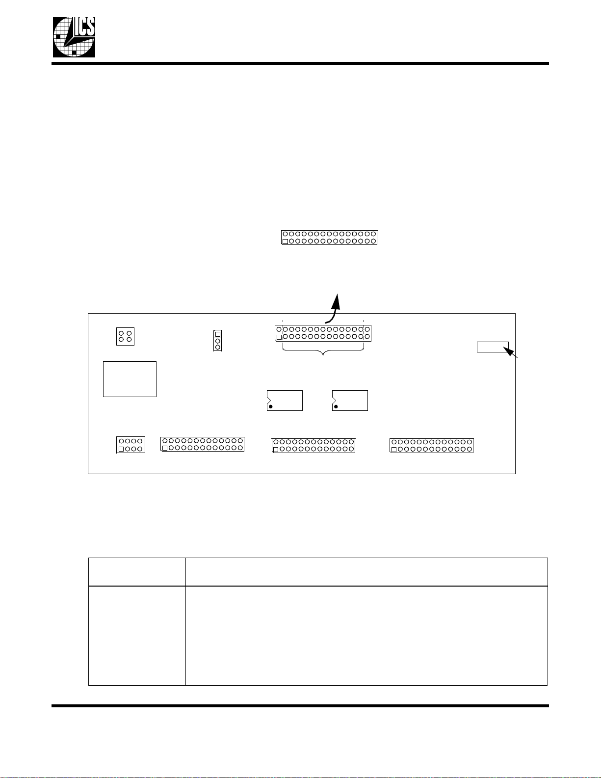
Chapter 1 Daughterboard Layouts
1531DaRevA 6/13/00 Copyright © 2000 Integrated Circuit Systems, Inc. All rights reserved. June, 2000
3
ICS1531 Daughterboard – Preliminary
JP7 Jumper 7.
Controls voltage to an LCD panel as follows:
•Pins 1 and 3 = Ground
•Pin 2 = +12 V
•Pin 4 = +5 V
JP8 Jumper 8.
Controls voltage to JP9 as follows:
•Pins 1 and 2 = +3.3 V to JP9 pins 1 and 2
•Pins 2 and 3 = +5 V to JP9 pins 1 and 2
JP9 Jumper 9.
Alternative connector for low-voltage differential signals (LVDS).
JP10 Jumper 10.
Selects input voltage to LVDS Daughterboard as follows:
•Pins 1 and 3 = +5 V
•Pins 2, 4, 6, 8 = Ground
•Pins 5 and 7 = +12 V
Serial number of
Daughter Board Serial number.
Unique serial number, located near the right top side of the LVDS Daughterboard.
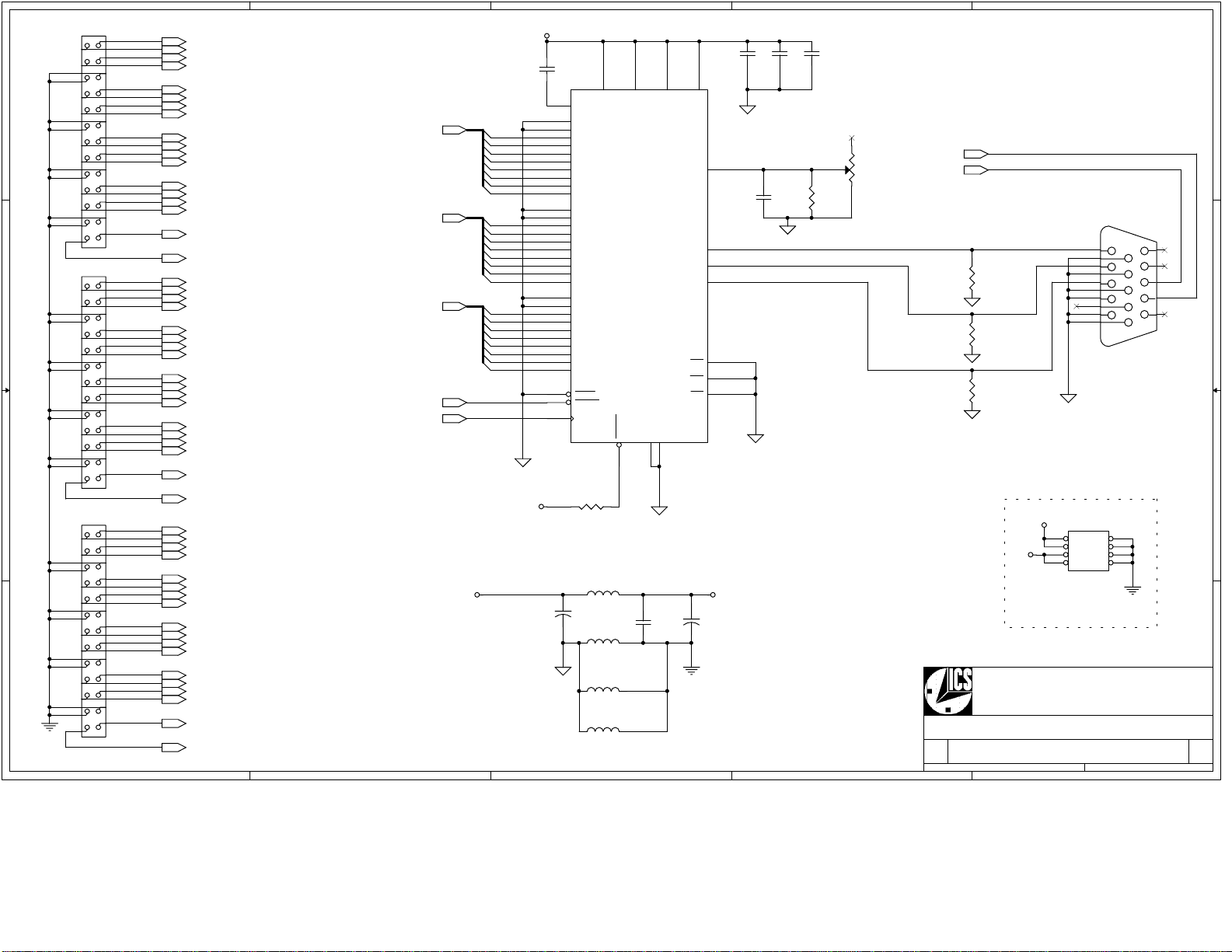
U13 Integrated Circuit 13.
LT1086CTvoltage regulator. Provides +3.3-V operating voltage to U14 and U15.
U14, U15 Integrated Circuit 14, 15
Low-voltage differential signaling (LVDS) transmitters.
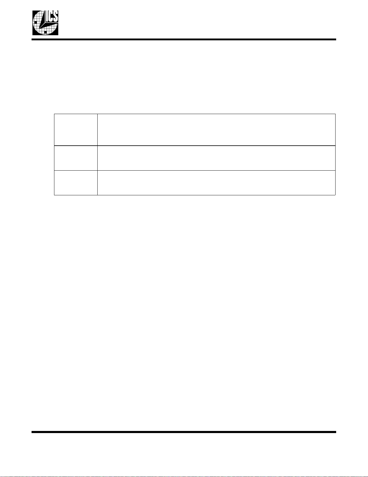
Table 1-1. LVDS Daughterboard Components (Continued)
Component #
and Label (If Any) Component Name, Function, and Settings
Pin Number
and Name Function Pin Number
and Name Function
1 - V5 / V3.3 Connects to JP8 Pin2 to
select either 5 or 3.3 V 16 - GND Ground
2 - V5 / V3.3 17 - TXE 0p Transmit Even 0 +
3 - GND Ground 18 - TXE 0m Transmit Even 0 -
4 - GND Ground 19 - TXE 1p Transmit Even 1 +
5 - TXO 0p Transmit Odd 0 + 20 - TXE 1m Transmit Even 1 -
6 - TXO 0m Transmit Odd 0 - 21 - TXE 2p Transmit Even 2 +
7 - TXO 1p Transmit Odd 1 + 22 - TXE 2m Transmit Even 2 -
8 - TXO 1m Transmit Odd 1 - 23 - TXE 3p Transmit Even 3 +
9 - TXO 2p Transmit Odd 2 + 24 - TXE 3m Transmit Even 3 -
10 - TXO 2m Transmit Odd 2 - 25 - TXE Ckp Transmit Even Clock +
11 - TXO 3p Transmit Odd 3 + 26 - TXE Ckm Transmit Even Clock -
12 - TXO 3m Transmit Odd 3 - 27 - GND Ground
13 - TXO Ckp Transmit Clock + 28 - GND Ground
14 - TXO Ckm Transmit Clock - 29 - V12 +12 V
15 - GND Ground 30 - V12 +12 V