inforce 6309 User manual

Confidential and Proprietary –Inforce Computing, Inc.
NO PUBLIC DISCLOSURE PERMITTED: Please report postings of this document on public
Restricted Distribution: Not to be distributed to anyone who is not an employee of either Inforce
Computing or its subsidiaries without the express approval of Inforce Computing.
Not to be used, copied, reproduced, or modified in whole or in part, nor its contents revealed in
any manner to others without the express written permission of Inforce Computing, Inc.
Inforce Computing is a trademark of Inforce Computing Incorporated, registered in the United
States and other countries. All Inforce Computing Incorporated trademarks are used with
permission. Other product and brand names may be trademarks or registered trademarks of their
respective owners.
This technical data may be subject to U.S. and international export, re-export, or transfer
(“export”) laws. Diversion contrary to U.S. and international law is strictly prohibited.
Inforce Computing, Inc.
48820 Kato Road, # 600B
Fremont, CA 94538
U.S.A.
© 2018 Inforce Computing, Inc.
Inforce 6309™
User Guide
002685 Rev H
November 13, 2018
Submit technical questions at:
http://www.inforcecomputing.com/techweb/
Inforce 6309™ User Guide Revision History
002685 Rev H MAY CONTAIN U.S. AND INTERNATIONAL EXPORT CONTROLLED INFORMATION i
Confidential and Proprietary –Inforce Computing, Inc.
Provided under NDA
Revision History
Revision
Date
Description
Author
A
12/January/2016
Initial Release
DJ
B
11/April/2016
Updated Figures 1, 2, 3, 9, and 10
Updated Tables 1 and 2
Updated Section 4.1.8
DJ
C
7/July/2016
Added Section 3.4
DJ
D
25/April/2017
Updated Table 1(Temperature
Specifications) in Section 2.3
MSS
E
7/July/2017
Updated Preface & Section 1
MSS
F
24/October/2018
Updated Figure 1
Added section 3.4.3
DJ
G
6/November/2018
Updated Block Diagram with Crystals
Added Warning about RF interference
section 2.2
FCC warning sentence in 2.3
DD
H
13/November/2018
RED & CE Frequencies and Power
updated section 2.2
MM
Approval Record
Function
Name
Date
Checked By
SS/DJ
13/November/2018
Reviewed By
VPS
13/November/2018
Approved By
PSD
13/November/2018

Inforce 6309™ User Guide License Agreement
002685 Rev H MAY CONTAIN U.S. AND INTERNATIONAL EXPORT CONTROLLED INFORMATION ii
Confidential and Proprietary –Inforce Computing, Inc.
Provided under NDA
License Agreement
Your use of this document is subject to and governed by those terms and conditions in the Inforce
Computing Purchase and Software License Agreement for the APQ8016 based Inforce 6309 development
platform, which you or the legal entity you represent, as the case may be, accepted and agreed to when
purchasing a Inforce 6309 development platform from InforceComputing Inc. (“Agreement”). You may use
this document, which shall be considered part of the defined term “Documentation” for purposes of the
Agreement, solely in support of your permitted use of the Inforce 6309 development platform under the
Agreement. Distribution of this document is strictly prohibited without the express written permission of
InforceComputing Inc. and its respective licensors, which they can withhold, condition or delay in its sole
discretion.
InforceComputing is a trademark of InforceComputing Inc., registered in USA and other countries.
Qualcomm is a trademark of Qualcomm Inc, registered in the United States and other countries. Other
product and brand names used herein may be trademarks or registered trademarks of their respective
owners.
This document contains technical data that may be subject to U.S. and international export, re-export, or
transfer (“export”) laws. Diversion contrary to U.S. and international law is strictly prohibited.

Inforce 6309™ User Guide Preface
002685 Rev H MAY CONTAIN U.S. AND INTERNATIONAL EXPORT CONTROLLED INFORMATION iii
Confidential and Proprietary –Inforce Computing, Inc.
Provided under NDA
Preface
This User Guide familiarizes the end user with the specification, interfaces, setup, and usage of the Inforce
6309 board.
Intended Audience
This User Guide is intended for technically qualified personnel. It is not intended for general audiences.
Document Organization
The chapters in this document are arranged as follows:
1. Scope
2. Hardware Specification
3. System Setup and Usage
4. Appendix A
5. Contact Information
Conventions
The following conventions are used in this document:
CAUTION
Cautions warn the user about how to prevent damage to hardware or loss of data.
NOTE
Notes call attention to important information.
References
1. IFC6309X Schematics, 002546
2. IFC6309 Hardware Reference Manual, 002547
Note
This document is subject to change without notice.
Support Information
Every effort has been made to ensure the accuracy of the User Guide. If you have any comments,
questions, or ideas regarding this document, contact Inforce’s technical support at:
techsupport@inforcecomputing.com

Inforce 6309™ User Guide Terminology
002685 Rev H MAY CONTAIN U.S. AND INTERNATIONAL EXPORT CONTROLLED INFORMATION iv
Confidential and Proprietary –Inforce Computing, Inc.
Provided under NDA
Terminology
The table below gives descriptions to some common terms used in the User Guide.
Term
Description
CSI
Camera Serial Interface
DDR
Double Data Rate
DSI
Display Serial Interface
eMMC
Embedded Multimedia Card
HD
High Definition
HDMI
High-Definition Multimedia Interface
I2C
Inter-Integrated Circuit
JTAG
Joint Test Action Group
LED
Light-Emitting Diode
MAC
Media Access Control
MIPI
Mobile Industry Processor Interface
OS
Operating System
OTG
On The Go
PCIe
Peripheral Component Interconnect Express
SATA
Serial Advanced Technology Attachment
SBC
Single Board Computer
SDC
Secure Digital Controller
SPI
Serial Peripheral Interface
UART
Universal Asynchronous Receiver Transmitter
USB
Universal Serial Bus

Inforce 6309™ User Guide Table of Contents
002685 Rev H MAY CONTAIN U.S. AND INTERNATIONAL EXPORT CONTROLLED INFORMATION v
Confidential and Proprietary –Inforce Computing, Inc.
Provided under NDA
Table of Contents
1. SCOPE.................................................................................................................................................1
2. HARDWARE SPECIFICATION ...........................................................................................................2
2.1 INTRODUCTION ................................................................................................................................2
2.2 ARCHITECTURE................................................................................................................................2
2.3 SYSTEM SPECIFICATION ................................................................................................................3
2.4 ELECTRICAL CHARACTERISTICS ..................................................................................................4
2.5 BOARD LAYOUT AND SUBSYSTEMS.............................................................................................4
3. SYSTEM SETUP AND USAGE...........................................................................................................6
3.1 HARDWARE SETUP..........................................................................................................................6
3.2 HARDWARE OPERATION.................................................................................................................6
3.2.1 CONFIGURATION SWITCHES..................................................................................................6
3.2.2 LED INDICATIONS .....................................................................................................................8
3.2.3 CONNECTOR COORDINATES..................................................................................................9
3.2.4 STEPS TO BOOT INFORCE 6309 SBC...................................................................................10
3.3 POWER MEASUREMENT...............................................................................................................11
3.3.1 5V RAIL.....................................................................................................................................11
3.3.2 VPH RAIL..................................................................................................................................11
3.4 ANTENNA CONFIGURATIONS.......................................................................................................11
3.4.1 GPS ANTENNA SELECTION...................................................................................................12
3.4.2 WI-FI ANTENNA SELECTION..................................................................................................12
3.4.3 WIFI / BT RF TX SPECFICIATIONS.........................................................................................13
4. APPENDIX A......................................................................................................................................14
4.1 CONNECTOR PIN ASSIGNMENTS ................................................................................................14
4.1.1 EXPANSION CONNECTOR.....................................................................................................14
4.1.2 ADD-ON INTERFACE PINOUT#...............................................................................................15
4.1.3 FRONT PANEL HEADER PINOUT...........................................................................................16
4.1.4 MIPI CAMERA INTERFACE PINOUT#.....................................................................................17
4.1.5 LVDS INTERFACE PINOUT#....................................................................................................18
4.1.6 DEBUG UART INTERFACE PINOUT.......................................................................................19
4.1.7 I2S INTERFACE........................................................................................................................19
4.1.8 JTAG INTERFACE....................................................................................................................20
4.1.9 BATTERY INTERFACE PINOUT..............................................................................................21
4.1.10 RF CONNECTORS#................................................................................................................21
5. CONTACT INFORMATION ...............................................................................................................22

Inforce 6309™ User Guide Table of Figures
002685 Rev H MAY CONTAIN U.S. AND INTERNATIONAL EXPORT CONTROLLED INFORMATION vi
Confidential and Proprietary –Inforce Computing, Inc.
Provided under NDA
Table of Figures
Figure 1: Block Diagram................................................................................................................................2
Figure 2: Inforce 6309 Board Locations (Top View) .....................................................................................4
Figure 3: Inforce 6309 Board Locations (Bottom View)................................................................................5
Figure 4: Configuration Switch SW4.............................................................................................................6
Figure 5: LED Locations on the Board..........................................................................................................8
Figure 6: Top Connector Coordinates...........................................................................................................9
Figure 7: Bottom Connector Coordinates .....................................................................................................9
Figure 8: Lock Screen Display....................................................................................................................10
Figure 9: 5V Current Measurement ............................................................................................................11
Figure 10: VPH Current Measurement .......................................................................................................11
Figure 11: GPS Antenna Topology.............................................................................................................12
Figure 12: Wi-Fi Antenna Topology ............................................................................................................12
Figure 13: Expansion Connector ................................................................................................................14
Figure 14 : Add-On Interface Header..........................................................................................................15
Figure 15: Front Panel Header....................................................................................................................16
Figure 16: MIPI Camera Connector............................................................................................................17
Figure 17: LVDS Connector........................................................................................................................18
Figure 18 : Debug Header...........................................................................................................................19
Figure 19 : I2S Header................................................................................................................................19
Figure 20 : JTAG Header............................................................................................................................20
Figure 21 : Battery HDR..............................................................................................................................21
Figure 22 : RF Connectors..........................................................................................................................21

Inforce 6309™ User Guide Table of Tables
002685 Rev H MAY CONTAIN U.S. AND INTERNATIONAL EXPORT CONTROLLED INFORMATION vii
Confidential and Proprietary –Inforce Computing, Inc.
Provided under NDA
Table of Tables
Table 1: System Hardware Specification......................................................................................................3
Table 2: Inforce 6309 Board Locations.........................................................................................................5
Table 3: Boot Selection.................................................................................................................................7
Table 4: USB Mode Selection.......................................................................................................................7
Table 5: Display Selection.............................................................................................................................7
Table 6: Auto Boot Selection.........................................................................................................................7
Table 7: LED Indications...............................................................................................................................8
Table 8: GPS Antenna Selection Configurations........................................................................................12
Table 9: Wi-Fi Antenna Selection Configurations.......................................................................................13
Table 10: Connector J8 Pinout ...................................................................................................................14
Table 11: Connector P6 Pinout...................................................................................................................15
Table 12: Connector P1 Pinout...................................................................................................................16
Table 13: Connector J11/12 Pinout ............................................................................................................17
Table 14 : Connector P3 Pinout..................................................................................................................18
Table 15 : Connector P2 Pinout..................................................................................................................19
Table 16 : Connector P5 Pinout..................................................................................................................19
Table 17: Connector P4 Pinout...................................................................................................................20
Table 18 : Connector J14 Pinout ................................................................................................................21

Inforce 6309™ User Guide Scope
002685 Rev H MAY CONTAIN U.S. AND INTERNATIONAL EXPORT CONTROLLED INFORMATION 1
Confidential and Proprietary –Inforce Computing, Inc.
Provided under NDA
1. SCOPE
This document describes the system setup and usage of Qualcomm Snapdragon 410 processor-based
Inforce 6309 Single Board Computer (SBC).
Anti-Static Handling Procedures
SBC has exposed PCB and chips. Accordingly, proper anti-static precautions should be employed when
handling the kit, including:
Use a grounded anti-static mat
Use a grounded wrist or foot strap
Hardware Identification Labels
Labels are present on the Inforce 6309 board. The following information is conveyed on the Inforce 6309
board:
Serial Number
Ethernet MAC Address
Wi-Fi and BT MAC Address
Product Revision

Inforce 6309™ User Guide Hardware Specification
002685 Rev H MAY CONTAIN U.S. AND INTERNATIONAL EXPORT CONTROLLED INFORMATION 2
Confidential and Proprietary –Inforce Computing, Inc.
Provided under NDA
2. HARDWARE SPECIFICATION
2.1 INTRODUCTION
The Inforce 6309 SBC can be used to develop, test, and deploy end-user product solutions around
Qualcomm Snapdragon 410, APQ8016 processor.
2.2 ARCHITECTURE
The functional diagram of the Inforce 6309 SBC is shown below.
Figure 1: Block Diagram

Inforce 6309™ User Guide Hardware Specification
002685 Rev H MAY CONTAIN U.S. AND INTERNATIONAL EXPORT CONTROLLED INFORMATION 3
Confidential and Proprietary –Inforce Computing, Inc.
Provided under NDA
2.3 SYSTEM SPECIFICATION
The following table shows the hardware specification of the Inforce 6309 SBC.
Table 1: System Hardware Specification
Processor and Peripherals
Processor
Qualcomm Snapdragon 410 APQ8016 (14mm × 12mm package)
Memory Devices
Main Memory
and Storage
1GB LPDDR, 8GB eMMC
I/O Interfaces
Interfaces
1× USB v2.0 (Debug), 2× USB v2.0 (Host), 1× HDMI, 1× LVDS#, 1× Dual MIPI-CSI#,1× UART,
1× UFL-Wi-Fi/BT#,1× UFL-GPS#, 1× uSD, 1× Headset Out, 1× Front-Panel Header, 1×
Expansion Header, 1× Add-On Interface#,1× Ethernet#, 1× I2S Header, 1× JTAG#, 1× Battery
Header
Form Factor
Mechanical
85mm × 54mm (credit-card form factor)
Power
Power Input
12V DC jack and 12V from add-on interface#
Others
Temperature
Specification
Commercial: 0°C to 70°C
Extended: –30°C to 85°C
Software
Operating System
Linux and Android
#Optional Interfaces.
NOTE
The system has been validated at ambient temperature ranges of 0°C to 55°C and –10ºC to 70ºC for commercial
and extended variants respectively.
The USB debug and the USB host/Ethernet interfaces are mutually exclusive.
HDMI and LVDS interfaces are mutually exclusive.
CAUTION
"This device complies with part 15 of the FCC Rules. Operation is subject to the following two conditions: (1) This
device may not cause harmful interference, and (2) this device must accept any interference received, including
interference that may cause undesired operation.”
This equipment has been tested and found to comply with the limits for a Class A digital device, pursuant to part
15 of the FCC Rules. These limits are designed to provide reasonable protection against harmful interference when
the equipment is operated in a commercial environment. This equipment generates, uses, and can radiate radio
frequency energy and, if not installed and used in accordance with the instruction manual, may cause harmful
interference to radio communications. Operation of this equipment in a residential area is likely to cause harmful
interference in which case the user will be required to correct the interference at his own expense.
Changes or modifications to this unit not expressly approved by the party responsible for compliance could void
the user’s authority to operate the equipment.
To comply with FCC's RF radiation exposure limits for general population/uncontrolled exposure, the antenna(s)
used for this transmitter must be installed to provide a separation distance of at least 20 cm from all persons and
must not be collocated or operating in conjunction with any other antenna or transmitter.
Inforce 6309™ User Guide Hardware Specification
002685 Rev H MAY CONTAIN U.S. AND INTERNATIONAL EXPORT CONTROLLED INFORMATION 4
Confidential and Proprietary –Inforce Computing, Inc.
Provided under NDA
2.4 ELECTRICAL CHARACTERISTICS
Power Supplies
The Inforce 6309 board is operated from the following sources:
12V DC jack/12V from add-on interface
3.7V battery operation (with limited functionality)
NOTE
12V is the default power supply
For battery operation:
Populate: R43, R275
Depopulate: R79, R51, R274
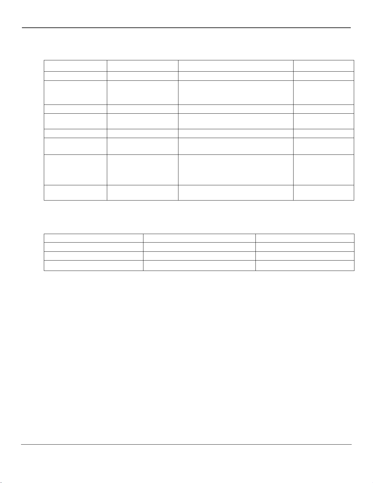
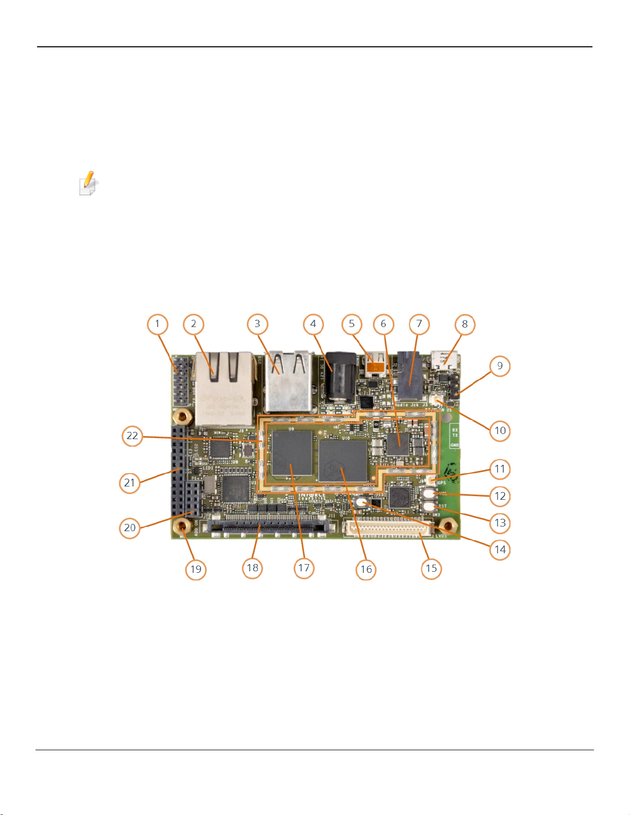
2.5 BOARD LAYOUT AND SUBSYSTEMS
Figure 2: Inforce 6309 Board Locations (Top View)
Inforce 6309™ User Guide Hardware Specification
002685 Rev H MAY CONTAIN U.S. AND INTERNATIONAL EXPORT CONTROLLED INFORMATION 5
Confidential and Proprietary –Inforce Computing, Inc.
Provided under NDA
Figure 3: Inforce 6309 Board Locations (Bottom View)
Table 2: Inforce 6309 Board Locations
No.
Description
No.
Description
1
Front Panel Header
16
APQ8016 Processor
2
RJ45 Ethernet Connector#
17
eMCP Memory
3
USB Type A Dual Connector
18
51-Pin Camera Interface#
4
DC Power Jack
19
Mounting Holes
5
uHDMI Connector
20
Add-On Interface for PoE/RS485 Card#
6
PM8916 PMIC
21
Expansion Interface
7
3.5mm Mic In–Speaker Out Combo Jack
22
Placeholders for Top Shield#
8
Micro-AB USB Connector
23
Placeholders for Bottom Shield#
9
Debug UART
24
BT/Wi-Fi PCB Antenna
10
BT/WLAN UFL Connector#
25
GPS PCB Antenna
11
GPS UFL Connector#
26
Boot Select/Configuration Switches
12
Vol + Button
27
Battery Header
13
Vol –Button
28
I2S Header
14
Power Button
29
JTAG Header#
15
LVDS Connector#
30
uSD Interface
#Optional Interfaces.
Inforce 6309™ User Guide System Setup and Usage
002685 Rev H MAY CONTAIN U.S. AND INTERNATIONAL EXPORT CONTROLLED INFORMATION 6
Confidential and Proprietary –Inforce Computing, Inc.
Provided under NDA
3. SYSTEM SETUP AND USAGE
3.1 HARDWARE SETUP
Set the proper boot configuration using the boot-selection switch on the board.
Refer to Section 3.2.1 for more details on various boot configuration settings.
Refer to LED locations on the board.
Refer to Section 3.2.4 for booting.
3.2 HARDWARE OPERATION
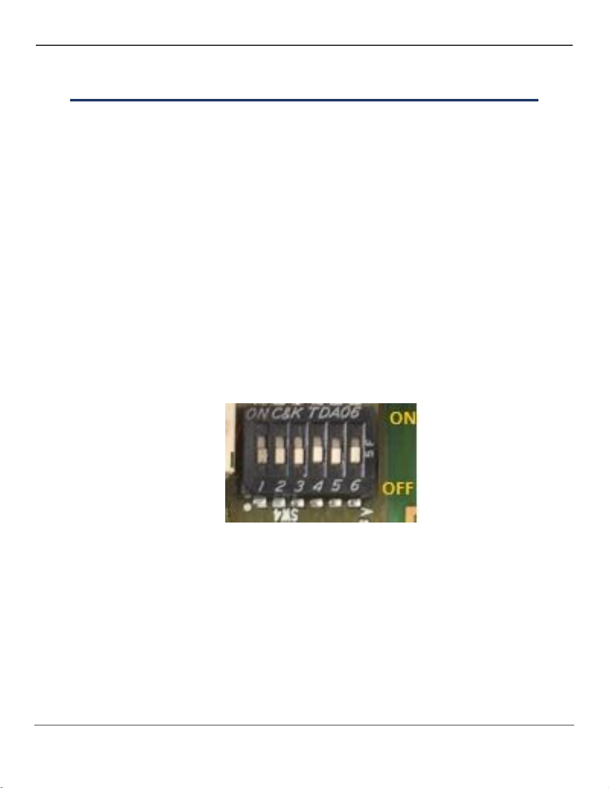
3.2.1 CONFIGURATION SWITCHES
SW4 switch on the Inforce 6309 board can be used for configuring the board for various modes of
operations.
Each position on SW4 has a defined functionality:
Boot configuration —Positions 1 and 2
USB mode selection —Position 3
Display selection —Position 4
Boot-on power —Position 5
Figure 4: Configuration Switch SW4
Inforce 6309™ User Guide System Setup and Usage
002685 Rev H MAY CONTAIN U.S. AND INTERNATIONAL EXPORT CONTROLLED INFORMATION 7
Confidential and Proprietary –Inforce Computing, Inc.
Provided under NDA
Table 3: Boot Selection
FORCED_USB_BOOT
(Position-1)
BOOT_CONFIG1
(Position-2)
Function
ON
X
Forces to QFIL mode
OFF
OFF
SDC1 (eMMC) followed by SDC2 (uSD) followed by USB
OFF
ON
SDC2 (uSD) followed by SDC1 (eMMC) followed by USB
Table 4: USB Mode Selection
USB_SW_SEL
(Position-3)
Function
ON
Forces to Host Mode
OFF
Auto Switch Mode
Table 5: Display Selection
DSI_SELECT_SW
(Position-4)
Function
ON
Forces HDMI Output
OFF
Auto Switch Mode
Table 6: Auto Boot Selection
CBLPWR_N
(Position-5)
Function
ON
Directly boots when powered UP
OFF
Waits for PWR button for booting
NOTE
“X” in the above table indicates a DON’T CARE situation, i.e., the functionality is independent
of that switch position.
Position 6 of SW4 is reserved for future use in the Inforce 6309 board.
Inforce 6309™ User Guide System Setup and Usage
002685 Rev H MAY CONTAIN U.S. AND INTERNATIONAL EXPORT CONTROLLED INFORMATION 8
Confidential and Proprietary –Inforce Computing, Inc.
Provided under NDA
3.2.2 LED INDICATIONS
Table 7: LED Indications
Ref. Des.
Function
LED State
DS1
User LED (PMIC GPIO 01)
User configurable
DS2
WLAN Status LED
ON: When WLAN is switched ON
DS3
BT Status LED
ON: When BT is switched ON
DS4
User LED (PMIC GPIO 02)
User configurable
DS5
User LED (APQ GPIO 120)
User configurable
DS6
User LED (APQ GPIO 95)
User configurable
D1
CPU RESET LED
ON: When CPU is out of RESET
Figure 5: LED Locations on the Board

Inforce 6309™ User Guide System Setup and Usage
002685 Rev H MAY CONTAIN U.S. AND INTERNATIONAL EXPORT CONTROLLED INFORMATION 9
Confidential and Proprietary –Inforce Computing, Inc.
Provided under NDA
3.2.3 CONNECTOR COORDINATES
Figure 6: Top Connector Coordinates
Figure 7: Bottom Connector Coordinates
Inforce 6309™ User Guide System Setup and Usage
002685 Rev H MAY CONTAIN U.S. AND INTERNATIONAL EXPORT CONTROLLED INFORMATION 10
Confidential and Proprietary –Inforce Computing, Inc.
Provided under NDA
3.2.4 STEPS TO BOOT INFORCE 6309 SBC
1. Remove the Inforce 6309 board carefully from the anti-static bag.
NOTE
Handle with care, while plugging, to avoid physical damage.
2. Connect the display through HDMI or LVDS interfaces.
3. Configure the boot and selection switches.
4. Connect the 12V power adapter to the wall socket.
5. Switch ON the power to the wall socket and press the POWER button, if the board is not in the
auto-power ON mode.
Android Version: After a few minutes, the "android" logo followed by the lock screen will be
displayed on the screen as shown in Figure 8.
NOTE
Carefully connect the DC connector to the jack provided on the board.
Once the processor is out of reset, D1 LED will glow.
CAUTION
Use only the DC adaptor provided by Inforce Computing.
Do not use the third party DC adaptor without our technical support, as it may damage
your board.
Figure 8: Lock Screen Display
NOTE
First time booting might take longer than the normal booting.
Screenshots shown above are for reference only; the actual display may vary depending
on the software release.
Inforce 6309™ User Guide System Setup and Usage
002685 Rev H MAY CONTAIN U.S. AND INTERNATIONAL EXPORT CONTROLLED INFORMATION 11
Confidential and Proprietary –Inforce Computing, Inc.
Provided under NDA
3.3 POWER MEASUREMENT
The Inforce 6309 board has a current sense resistor and test points on 5V and 3.7V rails for current/power
measurement.
3.3.1 5V RAIL
TP5 and TP6 shall be used for the current measurement.
Both are on the bottom side of the Inforce 6309 board.
Figure 9: 5V Current Measurement
3.3.2 VPH RAIL
TP7 and TP8 shall be used for the current measurement.
Both are on the bottom side of the Inforce 6309 board.
Figure 10: VPH Current Measurement
3.4 ANTENNA CONFIGURATIONS
Both GPS and Wi-Fi interfaces have provision for onboard PCB antenna and external Antenna.

Inforce 6309™ User Guide System Setup and Usage
002685 Rev H MAY CONTAIN U.S. AND INTERNATIONAL EXPORT CONTROLLED INFORMATION 12
Confidential and Proprietary –Inforce Computing, Inc.
Provided under NDA
Default Antenna Configurations are given below:
Wi-Fi Interface, Onboard PCB Antenna is default.
GPS Interface, external antenna connector is default.
3.4.1 GPS ANTENNA SELECTION
Figure 11: GPS Antenna Topology
Refer configurations listed below to change the default GPS antenna path.
Table 8: GPS Antenna Selection Configurations
3.4.2 WI-FI ANTENNA SELECTION
Figure 12: Wi-Fi Antenna Topology
Table of contents
Other inforce Motherboard manuals

Popular Motherboard manuals by other brands


Asus
Asus STRIX B250G GAMING quick start guide

Microchip Technology
Microchip Technology MCP19117 user guide

Texas Instruments
Texas Instruments bq24295EVM-549 user guide

MSI
MSI H310M PRO-M2 user guide

Texas Instruments
Texas Instruments TMUX-24PW-EVM user guide

NXP Semiconductors
NXP Semiconductors LPC55S36-EVK quick start guide