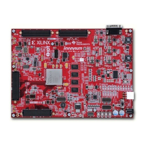
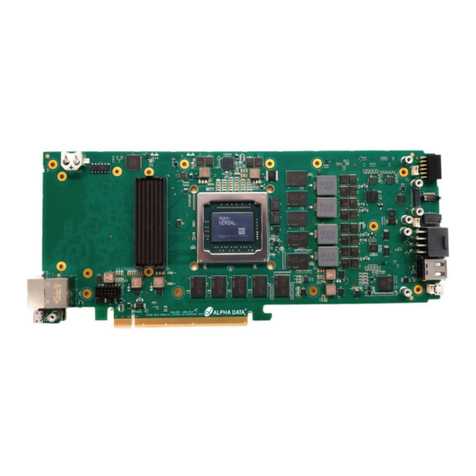
Inrevium TB-7VX-690T-PCIEXP Instructions for use

TB-7VX-690T/980T/1140T-PCIEXP Hardware User’s Manual
1
Rev.
1.0
4
TB-7VX-690T/980T/1140T-PCIEXP
Hardware User’s Manual
Rev.1.04

TB-7VX-690T/980T/1140T-PCIEXP Hardware User’s Manual
2
Rev.
1.0
4
Revision History
Version Date Description Publisher
Rev.1.0 2013/5/28 Preliminary Yanagisawa
Rev.1.01 2013/12/9 Release Version Yoshioka
Rev.1.02 2014/0318
Modified worng informations Yoshioka
Rev.1.03 2014/10/7 Additional specification based on FMC4 limitation Yoshioka
Rev.1.04 2014/10/27
Added Section 9 Initial Switch Settings Yoshioka

TB-7VX-690T/980T/1140T-PCIEXP Hardware User’s Manual
3
Rev.
1.0
4
Table of Contents
1. Related Documents and Board Accessories...................................................................................... 8
2. Overview ............................................................................................................................................ 8
3. Feature............................................................................................................................................... 8
4. Block Diagram.................................................................................................................................... 9
5. External View of the Board............................................................................................................... 10
6. Board Specification........................................................................................................................... 10
7. Description of Each Component ...................................................................................................... 12
7.1. Power Supply Structure ............................................................................................................ 12
7.2. Oscillator ................................................................................................................................... 13
7.2.1. Programmable clock generator.......................................................................................... 15
7.2.2. Clock Switch ...................................................................................................................... 16
7.3. FMC Connector Interface.......................................................................................................... 17
7.3.1. FMC1 HPC Connector (High-Pin Count)........................................................................... 18
7.3.2. FMC2 HPC Connector (High-Pin Count)........................................................................... 24
7.3.3. FMC3 HPC Connector (High-Pin Count)........................................................................... 30
7.3.4. FMC4 HPC Connector (High-Pin Count)........................................................................... 36
7.4. DDR3 SO-DIMM Interface ........................................................................................................ 42
7.5. PCI Express Edge Interface...................................................................................................... 49
7.6. PMOD Interface ........................................................................................................................ 51
7.7. QSPI-FLASH............................................................................................................................. 52
7.8. USB3.0...................................................................................................................................... 53
7.9. LED ........................................................................................................................................... 54
7.10. GPIO Interface....................................................................................................................... 55
7.11. DIPSW................................................................................................................................... 56
7.12. PUSHSW............................................................................................................................... 57
7.13. Power Connector for FAN ..................................................................................................... 58
7.14. Battery Control....................................................................................................................... 58
7.15. XADC Pinheader................................................................................................................... 59
8. Configuration.................................................................................................................................... 60
9. Initial Settings................................................................................................................................... 60

TB-7VX-690T/980T/1140T-PCIEXP Hardware User’s Manual
4
Rev.
1.0
4
List of Figures
Figure 4-1 Block Diagram .................................................................................................................. 9
Figure 5-1 Component Side of the Board ........................................................................................ 10
Figure 6-1 Board Dimension Diagram...............................................................................................11
Figure 7-1 Power Supply Structure.................................................................................................. 12
Figure 7-2 Clock Structure ............................................................................................................... 13
Figure 7-3 Programable Clock Connection...................................................................................... 15
Figure 7-4 Connection of clock switch ............................................................................................. 16
Figure 7-5 High-Pin Count Pin Layout ............................................................................................. 17
Figure 7-6 DIMM1 and DIMM2......................................................................................................... 42
Figure 7-7 QSPI Layout ................................................................................................................... 52
Figure 7-8 LED Layout..................................................................................................................... 54
Figure 7-9 GPIO Pin Layout............................................................................................................. 55
Figure 7-10 DIPSW Structure........................................................................................................... 56
Figure 7-11 PUSHSW Structure....................................................................................................... 57
Figure 7-12 Power Connector for FAN............................................................................................. 58
Figure 7-13 Battery........................................................................................................................... 58
Figure 7-14 XADC Structure ............................................................................................................ 59
Figure 9-1 location of SW and CN(Juspmer)................................................................................... 60
List of Tables
Table 7-1 Details of Onboard Oscillator ........................................................................................... 14
Table 7-2 Clock Selection................................................................................................................. 16
Table 7-3 FMC1 Connector Pinout................................................................................................... 18
Table 7-4 FMC2 Connector Pinout................................................................................................... 24
Table 7-5 FMC3 Connector Pinout................................................................................................... 30
Table 7-6 FMC4 Connector Pinout................................................................................................... 36
Table 7-7 DDR3 SO-DIMM-1 Pinout................................................................................................ 43
Table 7-8 DDR3 SO-DIMM-2 Pinout Table....................................................................................... 46
Table 7-9 PCI Express Edge Pinout Table....................................................................................... 49
Table 7-10 PCI Express Lane Width Configuration.......................................................................... 50
Table 7-11 PMOD Pinout Table........................................................................................................ 51
Table 7-12 QSPI Pinout Table.......................................................................................................... 52
Table 7-13 USB3.0 Pin Assign......................................................................................................... 53
Table 7-14 LED Pinout Table............................................................................................................ 54
Table 7-15 GPIO Pinout Table.......................................................................................................... 55
Table 7-16 DIPSW Pinout Table....................................................................................................... 56
Table 7-17 PUSHSW Pinout ............................................................................................................ 57
Table 7-18 External Power Supply Connector Pinout Table ............................................................ 58
Table 7-19 Battery Control signal Pinout Table................................................................................ 58
Table 7-20 XADC Pinout Table......................................................................................................... 59
Table 9-1 Initial Settings................................................................................................................... 60

TB-7VX-690T/980T/1140T-PCIEXP Hardware User’s Manual
5
Rev.
1.0
4
Introduction
Thank you for purchasing the TB-7VX-690T/980T/1140T-PCIEXP board. Before using the product, be
sure to carefully read this user manual and fully understand how to correctly use the product. First read
through this manual, then always keep it handy.
SAFETY PRECAUTIONS Be sure to observe these precautions
Observe the precautions listed below to prevent injuries to you or other personnel or damage to property.
Before using the product, read these safety precautions carefully to assure correct use.
These precautions contain serious safety instructions that must be observed.
After reading through this manual, be sure to always keep it handy.
The following conventions are used to indicate the possibility of injury/damage and classify precautions if
the product is handled incorrectly.
Indicates the high possibility of serious injury or death if the product is handled
incorrectly.
Indicates the possibility of serious injury or death if the product is handled
incorrectly.
Indicates the possibility of injury or physical damage in connection with houses or
household goods if the product is handled incorrectly.
The following graphical symbols are used to indicate and classify precautions in this manual.
(Examples)
Turn off the power switch.
Do not disassemble the product.
Do not attempt this.
Danger
Warning
Caution
!

TB-7VX-690T/980T/1140T-PCIEXP Hardware User’s Manual
6
Rev.
1.0
4
In the event of a failure, disconnect the power supply.
If the product is used as is, a fire or electric shock may occur. Disconnect the power supply
immediately and contact our sales personnel for repair.
If an unpleasant smell or smoking occurs, disconnect the power supply.
If the product is used as is, a fire or electric shock may occur. Disconnect the power supply
immediately. After verifying that no smoking is observed, contact our sales personnel for
repair.
Do not disassemble, repair or modify the product.
Otherwise, a fire or electric shock may occur due to a short circuit or heat generation. For
inspection, modification or repair, contact our sales personnel.
Do not touch a cooling fan.
As a cooling fan rotates in high speed, do not put your hand close to it. Otherwise, it may
cause injury to persons. Never touch a rotating cooling fan.
Do not place the product on unstable locations.
Otherwise, it may drop or fall, resulting in injury to persons or failure.
If the product is dropped or damaged, do not use it as is.
Otherwise, a fire or electric shock may occur.
Do not touch the product with a metallic object.
Otherwise, a fire or electric shock may occur.
Do not place the product in dusty or humid locations or where water may
splash.
Otherwise, a fire or electric shock may occur.
Do not get the product wet or touch it with a wet hand.
Otherwise, the product may break down or it may cause a fire, smoking or electric shock.
Do not touch a connector on the product (gold-plated portion).
Otherwise, the surface of a connector may be contaminated with sweat or skin oil, resulting
in contact failure of a connector or it may cause a malfunction, fire or electric shock due to
static electricity.
Warning
!
!
!
!
!
!
!

TB-7VX-690T/980T/1140T-PCIEXP Hardware User’s Manual
7
Rev.
1.0
4
Do not use or place the product in the following locations.
Humid and dusty locations
Airless locations such as closet or bookshelf
Locations which receive oily smoke or steam
Locations exposed to direct sunlight
Locations close to heating equipment
Closed inside of a car where the temperature becomes high
Staticky locations
Locations close to water or chemicals
Otherwise, a fire, electric shock, accident or deformation may occur due to a short circuit or heat
generation.
Do not place heavy things on the product.
Otherwise, the product may be damaged.
■Disclaimer
This product is an evaluation board for Xilinx Virtex-7 FPGA. Tokyo Electron Device Limited assumes no
responsibility for any damages resulting from the use of this product for purposes other than those
stated.
Even if the product is used properly, Tokyo Electron Device Limited assumes no responsibility for any
damages caused by:
(1) Earthquake, thunder, natural disaster or fire resulting from the use beyond our responsibility, acts by
a third party or other accidents, the customer’s willful or accidental misuse or use under other
abnormal conditions.
(2) Secondary impact arising from use of this product or its unusable state (business interruption or
others)
(3) Use of this product against the instructions given in this manual.
(4) Malfunctions due to connection to other devices.
Tokyo Electron Device Limited assumes no responsibility or liability for:
(1) Erasure or corruption of data arising from use of this product.
(2) Any consequences or other abnormalities arising from use of this product, or
(3) Damage of this product not due to our responsibility or failure due to modification
This product has been developed by assuming its use for research, testing or evaluation. It is not
authorized for use in any system or application that requires high reliability.
Repair of this product is carried out by replacing it on a chargeable basis, not repairing the faulty devices.
However, non-chargeable replacement is offered for initial failure if such notification is received within
two weeks after delivery of the product.
The specification of this product is subject to change without prior notice.
The product is subject to discontinuation without prior notice.
Caution
!
!

TB-7VX-690T/980T/1140T-PCIEXP Hardware User’s Manual
8
Rev.
1.0
4
1. Related Documents and Board Accessories
Related documents:
All documents relating to this board can be downloaded from our website. Please refer to attached paper
of the products.
Board Fixer:
Fan/heat sink set (Fan: 1, Heat sink: 1, M3 X 20 screw: 2, Washer: 2)
XH connector (JST: B3B-XH-A): 1
DDR3-SO-DIMM: 4G byte x2
Board Accessories:
Board foot set (Rubber foot: 7, M3 X 6 screw: 14, M3 X 10 spacer: 7)
AC/DC power supply (12V/15A): 1
AC power supply cable with a power switch: 1
DC power supply cable: 1
microSD card for FPGA Configuration (2G byte): 1
2. Overview
This board is the high-speed and high-density PCI Express Gen3 evaluation board equipped with Xilinx
Virtex7 Series FPGA “XC7VX690T/980T-2FFG1926 or 1140T-2FLG1926”.
3. Feature
- PCI Express Gen3(x8) interface
- High-Pin Count FMC connector x 4
Due to limitation of the number of FPGA pins, all the defined FMC connector pins are not
connected. For more information, refer to the corresponding connector pinout table contained
in this document.
FMC4 has a limitation of GTH usage. For more detail, please refer to section 7.3.4
- DDR3 SO-DIMM: 4GB x 2
- QSPI Flash for user application
- USB 3.0 device connector
- PMOD connector
- Various clock sources
- For operation: PushSWs, DipSWs, PinHeaders
- For monitoring: LEDs
- Configuration from microSD Card(Spartan3 FPGA is configuration controller)
- Configuration from BPI Flash(Spartan3 FPGA is configuration controller)
- JTAG interface to Virtex-7 FPGA directly.

TB-7VX-690T/980T/1140T-PCIEXP Hardware User’s Manual
9
Rev.
1.0
4
4. Block Diagram
The following figure shows the block diagram of this board.
FPGA
XC7VX690T/
VX980T
VX1140T
DDR3SO-DIMM#1(4GB)
[JAE]
MM80-204B1-1
CLK,ADDR,CMD
DATA[63:0],DQS,DM
DDR3SO-DIMM#2(4GB)
[JAE]
MM80-204B1-E1
CLK,ADDR,CMD
DATA[63:0],DQS,DM
PCIEExpress
Gen3
Edgex8
CLK
JitterAttenuator
[IDT]
ICS874003DGI-02
8pair
8pair
MicroSD
config
Cotroller
XC3S400AN-
5FGG400C
MicroSDConnector
[Hirose]
DM3AT-SF-PEJM5
ModeSwitch
[Copal]
SA-7050B
AREASwitch
[Copal]
SA-7050B
OSC50MHz
[Tamadevice]
CX104BC
50.000MHZ
PushSwitch
[Alps]
SKQYAAE010
I2CPinHeader
[Fci]
68001-104HLF
NorFlash
[Micron]
PC28F00AG18FE
SPIFlash
[Micron]
M25P40-
VMN6TPB
USB3.0
[Cypress]
CYUSB3014
-BZXI
OSC233MHz
[IDT]
4MA233333Z4AACUGI
OSC233MHz
[IDT]
4MA233333Z4AACUGI
OSC200MHz
[IDT]
4MA200000Z4AACUGI
OSC25MHz
[TXC]
7C-25.000MBA-T
ProgrammableCLK
[IDT]
ICS849N202I
Xtal40MHz
[TXC]
7M-40.000MAHE-T
CLKbuffer
[IDT]
ICS854104AGLF
FMC1(Highpincount)
[Samtec]
ASP-134486-01
IO(GTH):10CH
GC:2pair/IO:34pair
CLK(GTH):2pair
CLKSwitch
[Ti]
SN65LVDS250DBT
MMCXconnector
[Samtec]
MMCX-J-P-H-ST-TH1
MMCXconnector
[Samtec]
MMCX-J-P-H-ST-TH1
FMC2(Highpincount)
[Samtec]
ASP-134486-01
IO(GTH):10CH
GC:2pair/IO:34pair
CLK(GTH):2pair
CLKSwitch
[Ti]
SN65LVDS250DBT
MMCXconnector
[Samtec]
MMCX-J-P-H-ST-TH1
MMCXconnector
[Samtec]
MMCX-J-P-H-ST-TH1
FMC3(Highpincount)
[Samtec]
ASP-134486-01
IO(GTH):10CH
GC:2pair/IO:34pair
CLK(GTH):2pair
CLKSwitch
[Ti]
SN65LVDS250DBT
MMCXconnector
[Samtec]
MMCX-J-P-H-ST-TH1
MMCXconnector
[Samtec]
MMCX-J-P-H-ST-TH1
FMC4(Highpincount)
[Samtec]
ASP-134486-01
IO(GTH):10CH
GC:2pair/IO:34pair
CLK(GTH):2pair
CLKSwitch
[Ti]
SN65LVDS250DBT
MMCXconnector
[Samtec]
MMCX-J-P-H-ST-TH1
MMCXconnector
[Samtec]
MMCX-J-P-H-ST-TH1
JTAGconnector
[Molex]
87832-1420
Systemmonitor
connector[Fci]
67997-114HLF
PMODconnector
[Samtec]
SSW-106-01-F-D
FANconnector
[JST]
B3B-XH-A
QSPIFlash
[Micron]
N25Q512A11G1240F
MMCXconnector
[Samtec]
MMCX-J-P-H-ST-TH1
MMCXconnector
[Samtec]
MMCX-J-P-H-ST-TH1
OSCsocket
[Aries]
1108800
LEDx12
[Rohm]
SML-310MT
DipSwitchx12
[Copal]
CHS-04B
PinHeaderx16
[Fci]
68001-110HLF
PushSwitchx4
[Alps]
SKQYAAE010
OSC200MHz
CL284BB-200.000MHz
OSC200MHz
CL284BB-200.000MHz
OSC200MHz
CL284BB-200.000MHz
Figure 4-1 Block Diagram

TB-7VX-690T/980T/1140T-PCIEXP Hardware User’s Manual
10
Rev.
1.0
4
5. External View of the Board
The following figures show the external views of the board.
Figure 5-1 Component Side of the Board
6. Board Specification
External Dimensions: W:312mm x H:130mm (non-compliance with PCI-Express specification)
Number of Layers: 16 Layers
Board Thickness: 1.7 mm
Material: FR-5
FPGA: Xilinx XC7VX690T/980T-2FFG1926, XC7VX1140T-2FLG1926
BPI-FLASH: Micron PC28F00AG 18FE
QSPI-FLASH: Micron N25Q512A11G1240F
FMC Connector (High-Pin): Samtec ASP-134486-01
DDR3 SO-DIMM: JAE MM80-204B1-1, MM80-204B1-E
MMCX Connector: Samtec MMCX-J-P-H-ST-TH1
PMOD Connector: Samtec SSW-106-01-F-D
USB3.0 Connector: TE Connectivity 1932259-1
General-Purpose I/F(GPIO):FCI 68001-110HLF

TB-7VX-690T/980T/1140T-PCIEXP Hardware User’s Manual
11
Rev.
1.0
4
Figure 6-1 Board Dimension Diagram

TB-7VX-690T/980T/1140T-PCIEXP Hardware User’s Manual
12
Rev.
1.0
4
7. Description of Each Component
7.1. Power Supply Structure
The following figure provides the internal power supply structure. The power is provided through a 12V
ATX power connector.
Power
Connector FPGA:Vccint
1.0V/37.5A
LTC3855
LTC3600 FPGA:Vccauxio
2.0V/1.28A
LTM4627 FMC-OptionBoard
FPGA:Vcco
1.8V/13.2A
LTM4620
FPGA:Vcco
1.8V/4.9A
FPGA:Vcco
1.5V/8.43A
LTM4628
FPGA:Vccaux
1.8V/3.4A
VCC_3P3V
3.3V/3.07A
LTC3025 MGTVCCAUX_1P8V
1.8V/0.13A
LTC3617 DDR3_0P75V
0.75V/2.7A
TLV70218DBV V7_VCCADC_1P8V
1.8V/0.2A
REF3012 V7_VREFP_1P25V
1.25V/0.01A
LTM4627 MGTAVTT_1P2V
1.2V/4.6A
LT3070
LT3070 MGTAVCC_1P05V_L
1.05V/3.8A
LT3070 MGTAVCC_1P05V_R0
1.05V/1.9A
LT3070 MGTAVCC_1P05V_R1
1.05V/1.9A
LTC3600 S3_VCCINT_1P2V
1.2V/0.51A
LTM4627 FMC-OptionBoard
3.3V/12A
FMC-OptionBoard
12V/4A
Figure 7-1 Power Supply Structure

TB-7VX-690T/980T/1140T-PCIEXP Hardware User’s Manual
13
Rev.
1.0
4
7.2. Oscillator
This board provides the following clock sources.
U34
ClockBuffer
X10
40Mhz
P
N
P
N
C35:Bank_17(IO)
D35:Bank_17(IO)
P
N
P
N
U64
ClockSwitch
AD8:MGTREFCLK0P_114
AD7:MGTREFCLK0N_114
AF8:MGTREFCLK1P_114
AF7:MGTREFCLK1N_114
P
N
CN24
(FMC1_MMCX_CLK_P)
CN25
(FMC1_MMCX_CLK_N)
P
N
P
N
CN14
FMC1
G16:Bank_34(MC)
G15:Bank_34(MC)
K19:Bank_35(MC)
J19:Bank_35(MC)
P
N
P
N
U65
ClockSwitch
K8:MGTREFCLK0P_117
K7:MGTREFCLK0N_117
M8:MGTREFCLK1P_117
M7:MGTREFCLK1N_117
P
N
CN26
(FMC2_MMCX_CLK_P)
CN27
(FMC2_MMCX_CLK_N)
P
N
P
N
CN15
FMC2
P
N
K11:Bank_36(MC)
J11:Bank_36(MC) P
N
H28:Bank_16(MC)
H29:Bank_16(MC)
P
N
K37:MGTREFCLK0P_217
K38:MGTREFCLK0N_217
M37:MGTREFCLK1P_217
M38:MGTREFCLK1N_217
L21:Bank_33(MC)
K21:Bank_33(MC)
H19:Bank_35(MC)
H18:Bank_35(MC)
AD37:MGTREFCLK0P_214
AD38:MGTREFCLK0N_214
AF37:MGTREFCLK1P_214
AF38:MGTREFCLK1N_214
CN30
(FMC4_MMCX_CLK_P)
CN31
(FMC4_MMCX_CLK_N)
L26:Bank_13(MC)
K27:Bank_13(MC)
K33:Bank_15(MC)
K34:Bank_15(MC)
FPGA
AR26:Bank_11(MC)
AT26:Bank_11(MC)
P
N
X7
OSC
200Mhz
AT20:Bank_31(MC)
AU20:Bank_31(MC)
X8 P
N
OSC
200Mhz
AU18:Bank_31(SC)
AU17:Bank_31(SC)
X9 P
N
OSC
200Mhz
CN23
PCIExpress edge
P
N
P
N
P
N
P
N
AP8:MGTREFCLK0P_112
AP7:MGTREFCLK0N_112
AT8:MGTREFCLK1P_112
AT7:MGTREFCLK1N_112
AV8:MGTREFCLK0P_111
AV7:MGTREFCLK0N_111
C33:Bank_17(MC)
C34:Bank_17(MC)
P
N
CN46(MMCX_CLK_P)
CN47(MMCX_CLK_N)
P
N
P
N
P
N
U53
ProgrammableClock
P
N
P
N
P
N
U66
ClockSwitch
P
N
CN28
(FMC3_MMCX_CLK_P)
CN29
(FMC3_MMCX_CLK_N)
P
N
P
N
CN16
FMC3
P
N
P
N
P
N
P
N
P
N
U67
ClockSwitch
P
N
P
N
P
N
CN17
FMC4
P
N
P
N
P
N
X11 OSC
25Mhz
U42
ClockBuffer
E33:Bank_17(MC)
U55
OSC
Socket Level
Shifter
U70
Figure 7-2 Clock Structure

TB-7VX-690T/980T/1140T-PCIEXP Hardware User’s Manual
14
Rev.
1.0
4
Table 7-1 Details of Onboard Oscillator
Source
Signal Name Signal
Format FPGA
Pin# Note
X7 DDR3_IF_1_CLK_200MHz_P /N LVDS AR26/AT26 DDR3_IF_1 system clock
X8 CLK_200M_P/N LVDS AT20/AU20 User clock
X9 DDR3_IF_2_CLK_200MHz_P/N LVDS AU18/AU17 DDR3_IF_2 system clock
CN23 PCIE_100M_REFCLK_P/N
PCIE_125M_REFCLK_P/N
PCIE_250M_REFCLK_P/N LVDS AP8/AP7
AT8/AT7
AV8/AV7
PIC Express Edge to
differential buffer
U55 V7_RSVCLK LVCMOS18 E33 OSC Socket spare clock
CN46
CN47 MMCX_CLK_P/N LVDS C33/C34 MMCX external supplied
clock
U53 PLL_CLK_P/N LVDS Programmable clock(U53)
generate device Source
clock is OSC or FPGA.
U64 FMC1_MGTREFCLK0_P/N
FMC1_MGTREFCLK1_P/N LVDS AD8/AD7
AF8/AF7
Programmable clock(U53)
or MMCX (CN24/CN25),
FMC1(CN14),
MGT reference clock 0/1
CN14 FMC1_CLK0_M2C_P/N
FMC1_CLK1_M2C_P/N LVDS G16/G15
K19/J19 FMC1 reference clock 0/1
U65 FMC2_MGTREFCLK0_P/N
FMC2_MGTREFCLK1_P/N LVDS K8/K7
M8/M7
Programmable clock(U53)
or MMCX (CN26/CN27 ),
FMC2(CN15),
MGT reference clock 0/1
CN15 FMC2_CLK0_M2C_P/N
FMC2_CLK1_M2C_P/N LVDS K11/J11
H28/H29 FMC2 reference clock 0/1
U66 FMC3_MGTREFCLK0_P/N
FMC3_MGTREFCLK1_P/N LVDS K37/K38
M37/M38
Programmable clock(U53)
or MMCX (CN28/CN29 )
FMC3(CN16)
MGT reference clock 0/1
CN16 FMC3_CLK0_M2C_P/N
FMC3_CLK1_M2C_P/N LVDS L21/K21
H19/H18 FMC3 reference clock 0/1
U67 FMC4_MGTREFCLK0_P/N
FMC4_MGTREFCLK1_P/N LVDS AD37/AD38
AF37/AF38
Programmable clock(U53)
MMCX (CN30/CN31 )
FMC4(CN17)
MGT reference clock 0/1
CN17 FMC4_CLK0_M2C_P/N
FMC4_CLK1_M2C_P/N LVDS L26/K27
K33/K34 FMC4 reference clock 0/1

TB-7VX-690T/980T/1140T-PCIEXP Hardware User’s Manual
15
Rev.
1.0
4
7.2.1. Programmable clock generator
This board has a programmable clock generater “ICS849N202I(U53)”for reference clock of Virtex-7
FPGA GTH Transceiver.
The initial setting is below.
ICS849N202I: 156.25MHz
SW5: all OFF.
Please used by default settings.
If using ICS849N202I for other frequency, please feel free to contact our support web
Figure 7-3 Programable Clock Connection
Output clock is distributed by Clock buffer(U34) then clocks are provide to each GTH group.

TB-7VX-690T/980T/1140T-PCIEXP Hardware User’s Manual
16
Rev.
1.0
4
7.2.2. Clock Switch
Reference clock of GTH is selectable by “SN65LVDS250(U64,U65,U66,U67)”
Clock Switch has 4 clock sources and select 2 clocks for GTH reference clock.
Figure 7-4 Connection of clock switch
Clock Sources
・FMCxx_CLK_P/N: From ICS849N202I programmable clock.
・FMCxx_MMCX_CLK_P/N: From MMCX(CN24,25/CN26,27/CN28,29/CN30.31).
・FMCxxx_GBTCLK0_M2C_P/N: From FMC(GBTCLK0_M2C_P/N)
・FMCxxx_GBTCLK1_M2C_P/N: From FMC(GBTCLK1_M2C_P/N)
Which Switch is related which FMC.
FMC1(CN14) : SW14
FMC2(CN15) : SW15
FMC3(CN16) : SW16
FMC4(CN17) : SW17
Table 7-2 Clock Selection
OUTPUT CHANNEL 1 OUTPUT CHANNEL 2
S10 S11 1Y/1Z S20 S21 2Y/2Z
OFF OFF 1A/1B OFF OFF 1A/1B
OFF ON 2A/2B OFF ON 2A/2B
ON OFF 3A/3B ON OFF 3A/3B
ON ON 4A/4B ON ON 4A/4B

TB-7VX-690T/980T/1140T-PCIEXP Hardware User’s Manual
17
Rev.
1.0
4
7.3. FMC Connector Interface
This board has 4 Samtec FMC connectors.
High-Pin Count: 4 (CN14,CN15,CN16,CN17)
The following provides the pinout table. Note that all pins are not connected to the FPGA.
Figure 7-5 High-Pin Count Pin Layout

TB-7VX-690T/980T/1140T-PCIEXP Hardware User’s Manual
18
Rev.
1.0
4
7.3.1. FMC1 HPC Connector (High-Pin Count)
The board uses the High-Pin Count connector. Due to limitation of the number of FPGA pins (Banks), all
FMC connector pins are not connected. The connector is interfaced as shown below.
HighSpead: TX 10ch, RX 10ch
LowSpead: LA 36Pair (include 2 pair clocks)
Table 7-3 FMC1 Connector Pinout
Bank
No.
Pin
No.
A
B
Pin
No.
Bank
No.
GND
1
RES1
MGTHRXP1_113
AL6 DP1_M2C_P
2
GND
MGTHRXN1_113
AL5 DP1_M2C_N
3
GND
GND 4
DP9_M2C_P Y4 MGTHRXP1_115
GND 5
DP9_M2C_N Y3 MGTHRXN1_115
MGTHRXP2_113
AJ6 DP2_M2C_P
6
GND
MGTHRXN2_113
AJ5 DP2_M2C_N
7
GND
GND 8
DP8_M2C_P AA6 MGTHRXP0_115
GND 9
DP8_M2C_N AA5 MGTHRXN0_115
MGTHRXP3_113
AH4 DP3_M2C_P
10
GND
MGTHRXN3_113
AH3 DP3_M2C_N
11
GND
GND 12
DP7_M2C_P AC6 MGTHRXP3_114
GND 13
DP7_M2C_N AC5 MGTHRXN3_114
MGTHRXP0_114
AG6 DP4_M2C_P
14
GND
MGTHRXN0_114
AG5 DP4_M2C_N
15
GND
GND 16
DP6_M2C_P AD4 MGTHRXP2_114
GND 17
DP6_M2C_N AD3 MGTHRXN2_114
MGTHRXP1_114
AE6 DP5_M2C_P
18
GND
MGTHRXN1_114
AE5 DP5_M2C_N
19
GND
GND 20
*1 GBTCLK1_M2C_P Clock Switch
GND 21
*1 GBTCLK1_M2C_N Clock Switch
MGTHTXP1_113 AL2 DP1_C2M_P
22
GND
MGTHTXN1_113
AL1 DP1_C2M_N
23
GND
GND 24
DP9_C2M_P AA2 MGTHTXP1_115
GND 25
DP9_C2M_N AA1 MGTHTXN1_115
MGTHTXP2_113 AK4 DP2_C2M_P
26
GND
MGTHTXN2_113
AK3 DP2_C2M_N
27
GND
GND 28
DP8_C2M_P AB4 MGTHTXP0_115
GND 29
DP8_C2M_N AB3 MGTHTXN0_115
MGTHTXP3_113 AJ2 DP3_C2M_P
30
GND
MGTHTXN3_113
AJ1 DP3_C2M_N
31
GND
GND 32
DP7_C2M_P AC2 MGTHTXP3_114
GND 33
DP7_C2M_N AC1 MGTHTXN3_114
MGTHTXP0_114 AG2 DP4_C2M_P
34
GND
MGTHTXN0_114
AG1 DP4_C2M_N
35
GND
GND 36
DP6_C2M_P AE2 MGTHTXP2_114
GND 37
DP6_C2M_N AE1 MGTHTXN2_114
MGTHTXP1_114 AF4 DP5_C2M_P
38
GND
MGTHTXN1_114
AF3 DP5_C2M_N
39
GND
GND 40
RES0

TB-7VX-690T/980T/1140T-PCIEXP Hardware User’s Manual
19
Rev.
1.0
4
Bank
No.
Pin
No.
C
D
Pin
No.
Bank
No.
GND
1
PG_C2M
MGTHTXP0_113 AN2 DP0_C2M_P 2 GND
MGTHTXN0_113 AN1 DP0_C2M_N 3 GND
GND 4 *1 GBTCLK0_M2C_P Clock Switch
GND 5 *1 GBTCLK0_M2C_N Clock Switch
MGTHRXP0_113 AM4 DP0_M2C_P 6 GND
MGTHRXN0_113 AM3 DP0_M2C_N 7 GND
GND 8 LA01_P_CC K16 34
GND 9 LA01_N_CC J16 34
34 J15 LA06_P 10 GND
34 H15 LA06_N 11 LA05_P K14 34
GND 12 LA05_N J14 34
GND 13 GND
34 G13 LA10_P 14 LA09_P C12 34
34 F13 LA10_N 15 LA09_N B12 34
GND 16 GND
GND 17 LA13_P U16 34
34 U15 LA14_P 18 LA13_N T16 34
34 T15 LA14_N 19 GND
GND 20 LA17_P_CC P14 34
GND 21 LA17_N_CC N14 34
34 T14 LA18_P_CC 22 GND
34 R14 LA18_N_CC 23 LA23_P K17 35
GND 24 LA23_N J17 35
GND 25 GND
35 L19 LA27_P 26 LA26_P J20 35
35 K18 LA27_N 27 LA26_N H20 35
GND 28 GND
GND 29 TCK
SCL 30 *2 TDI
SDA 31 *2 TDO
GND 32 3P3VAUX
GND 33 TMS
GA0 34 TRST_L
12P0V 35 GA1
GND 36 3P3V
12P0V 37 GND
GND 38 3P3V
3P3V 39 GND
GND 40 3P3V

TB-7VX-690T/980T/1140T-PCIEXP Hardware User’s Manual
20
Rev.
1.0
4
Bank
No.
P
in
No.
E
F
Pin
No.
Bank
No.
GND
1
PG_M2C
HA01_P_CC 2 GND
HA01_N_CC 3 GND
GND 4 HA00_P_CC
GND 5 HA00_N_CC
HA05_P 6 GND
HA05_N 7 HA04_P
GND 8 HA04_N
HA09_P 9 GND
HA09_N 10 HA08_P
GND 11 HA08_N
HA13_P 12 GND
HA13_N 13 HA12_P
GND 14 HA12_N
HA16_P 15 GND
HA16_N 16 HA15_P
GND 17 HA15_N
HA20_P 18 GND
HA20_N 19 HA19_P
GND 20 HA19_N
HB03_P 21 GND
HB03_N 22 HB02_P
GND 23 HB02_N
HB05_P 24 GND
HB05_N 25 HB04_P
GND 26 HB04_N
HB09_P 27 GND
HB09_N 28 HB08_P
GND 29 HB08_N
HB13_P 30 GND
HB13_N 31 HB12_P
GND 32 HB12_N
HB19_P 33 GND
HB19_N 34 HB16_P
GND 35 HB16_N
HB21_P 36 GND
HB21_N 37 HB20_P
GND 38 HB20_N
VADJ 39 GND
GND 40 VADJ
This manual suits for next models
2
Table of contents
Other Inrevium Computer Hardware manuals
Popular Computer Hardware manuals by other brands
powersoft
powersoft MiniMod 4 user guide
ekwb
ekwb EK-FC R9-390X TF5 Series INSTALLATION AND MOUNTING MANUAL

American Megatrends
American Megatrends MegaRAC G3 user guide
ARM
ARM DSTREAM DS-5 manual
Dialogic
Dialogic Dialogic Media Board DMV600BTEC Quick install card
DLP Design
DLP Design DLP-RFID2-EDK2 Setup procedure
