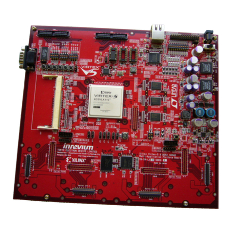
Inrevium TB-KU-060/075-ACDC8K Instructions for use

TB-KU-xxx-ACDC8K Hardware User Manual
1
Rev. 1.03
TB-KU-xxx-ACDC8K
Hardware User Manual
Rev. 1.03

TB-KU-xxx-ACDC8K Hardware User Manual
2
Rev. 1.03
Revision History
Version
Date
Description
Publisher
Rev. 1.00
2014/10/15
Initial Release
DM
Rev. 1.01
2015/01/19
Updated content with board pictures and FMC pinout
tables
DM
Rev. 1.02
2015/02/18
Updated Figure 4-1, 7-2, 7-6, 7-16
KM
Rev. 1.03
2015/07/21
Released for 060
Added Standoffs and Power Strip cord
Updated Figure 5-1, 7-6, 7-8, 7-9, 7-12
Updated Table 7-16, 7-22, 7-23
Added 8.1 Default Settings
Morita
Odajima

TB-KU-xxx-ACDC8K Hardware User Manual
3
Rev. 1.03
Table of Contents
1. Related Documents andAccessories ......................................................................................... 9
2. Overview...................................................................................................................................... 9
3. Feature ...................................................................................................................................... 10
4. Block Diagram ............................................................................................................................11
5. External View of the Board........................................................................................................ 12
6. Board Specifications.................................................................................................................. 13
7. Description of Components....................................................................................................... 16
7.1. Power Supply Structure............................................................................................................ 16
7.1.1. Power Sequencing............................................................................................................ 17
7.1.2. Power Input connectors.................................................................................................... 17
7.1.3. DC 4-pin Header and Binding Posts................................................................................. 18
7.1.4. Voltage Rails Test Points .................................................................................................. 19
7.1.5. Power and Miscellaneous LEDs....................................................................................... 20
7.1.6. Board Power Button.......................................................................................................... 21
7.1.7. FPGA HR Bank Voltage Selection.................................................................................... 21
7.1.8. HR Banks Voltage and SFP+ RX_LOS/TX_FAULT Selection.......................................... 21
7.2. FPGA Banks Assignments ....................................................................................................... 22
7.3. Clock System ........................................................................................................................... 23
7.3.1. VCCINT Clock Architecture .............................................................................................. 23
7.3.2. GTH Clocks ...................................................................................................................... 24
7.3.3. User Assigned Clocks....................................................................................................... 25
7.4. FMC Connector Interface......................................................................................................... 26
7.4.1. FMC HPC 0 (J1) ............................................................................................................... 26
7.4.2. FMC HPC 1 (J2) ............................................................................................................... 34
7.4.3. FMC HPC 2 (J5) ............................................................................................................... 41
7.4.4. FMC HPC 3 (J8) ............................................................................................................... 48
7.4.5. FMC HPC 4 (J11) ............................................................................................................. 55
7.4.6. FMC HPC 5 (J14) ............................................................................................................. 62
7.4.7. FMC HPC 6 (J19) ............................................................................................................. 69
7.5. DDR4 SDRAM.......................................................................................................................... 76
7.6. SFP+ Connectors..................................................................................................................... 77
7.7. USB to UART Controller........................................................................................................... 79
7.8. Battery...................................................................................................................................... 80
7.9. Dual Quad (x8) SPI Flash ........................................................................................................ 81
7.10. JTAG and Pmod Interface.................................................................................................... 82
7.10.1. JTAG Connector ............................................................................................................... 82
7.10.2. Pmod Interface ................................................................................................................. 83
7.11. General Purpose LEDs......................................................................................................... 84
7.12. General Purpose Switches................................................................................................... 85
7.12.1. DIP Switches..................................................................................................................... 85
7.12.2. Push Switches .................................................................................................................. 85
7.12.3. Jumper Switches .............................................................................................................. 86
8. Appendix.................................................................................................................................... 87
8.1. Default Settings........................................................................................................................ 87
8.2. Power Sequencer Timings ....................................................................................................... 88

TB-KU-xxx-ACDC8K Hardware User Manual
4
Rev. 1.03
List of Figures
Figure 4-1 Block Diagram .................................................................................................................11
Figure 5-1 Board Top View............................................................................................................... 12
Figure 6-1 Board Dimensions (inclusive of wastable substrate, top view)....................................... 14
Figure 6-2 Board Dimensions (inclusive of wastable substrate, bottom view)................................. 15
Figure 7-1 Power Supply Structure .................................................................................................. 16
Figure 7-2 Power Sequencer ........................................................................................................... 17
Figure 7-3 Power Input Circuit ......................................................................................................... 17
Figure 7-4 12VDC Input Connector and Binding Posts ................................................................... 18
Figure 7-5 Board Power Button........................................................................................................ 21
Figure 7-6 FPGA Banks Assignments.............................................................................................. 22
Figure 7-7 VCCINT Clock Synchronization...................................................................................... 23
Figure 7-8 GTH and MMCX Clocks Architecture ............................................................................. 24
Figure 7-9 User Assigned Clocks Architecture................................................................................. 25
Figure 7-10 High Pin Count FMC..................................................................................................... 26
Figure 7-11 FMC 0 to 6 SCL/SDA, GA0/GA1, TDI/TDO.................................................................. 32
Figure 7-12 DDR4 SDRAM Structure............................................................................................... 76
Figure 7-13 I2C MUX Hardware-selectable Address Pins............................................................... 77
Figure 7-14 USB UART Interface..................................................................................................... 79
Figure 7-15 Battery Circuit ............................................................................................................... 80
Figure 7-16 FPGASPI Flash Configuration Structure...................................................................... 81
Figure 7-17 Pmod Connection ......................................................................................................... 83
Figure 7-18 Jumper Switches Structure........................................................................................... 86
Figure 8-1 Jumper and Switch location (Component Side) ............................................................. 87
Figure 8-2 Power Sequencer Default Settings................................................................................. 88

TB-KU-xxx-ACDC8K Hardware User Manual
5
Rev. 1.03
List of Tables
Table 7-1 Voltage Rails Test Points.................................................................................................. 19
Table 7-2 Board LEDs...................................................................................................................... 20
Table 7-3 HR Banks Connected Peripherals ................................................................................... 21
Table 7-4 HR Banks Voltage and RX_LOS/TX_FAULT Selection ................................................... 21
Table 7-5 FMC 0 (J1) to FPGA Pinout.............................................................................................. 27
Table 7-6 FMC 1 (J2) to FPGA Pinout.............................................................................................. 35
Table 7-7 FMC 2 (J5) to FPGA Pinout.............................................................................................. 42
Table 7-8 FMC 3 (J8) to FPGA Pinout.............................................................................................. 49
Table 7-9 FMC 4 (J11) to FPGA Pinout............................................................................................ 56
Table 7-10 FMC 5 (J14) to FPGA Pinout.......................................................................................... 63
Table 7-11 FMC 6 (J19) to FPGA Pinout.......................................................................................... 70
Table 7-12 SFP+ I2C Bus Pin Assignment....................................................................................... 78
Table 7-13 RX_LOS, TX_FAULT and RS PinAssignment............................................................... 78
Table 7-14 Micro-USB Type B and AB Compatibility........................................................................ 79
Table 7-15 UART Interface Pin Assignment..................................................................................... 79
Table 7-16 SPI Flash Memory Pin Assignment................................................................................ 82
Table 7-17 Xilinx 14-pin JTAG Pinout............................................................................................... 82
Table 7-18 FPGA Bank 0 JTAG PinAssignment.............................................................................. 82
Table 7-19 Pmod Pin Assignment .................................................................................................... 83
Table 7-20 Uncommitted LEDs Pin Assignment .............................................................................. 84
Table 7-21 DIP Switches Pin Assignment ........................................................................................ 85
Table 7-22 Push-button Switches Pin Assignment........................................................................... 85
Table 7-23 Jumper Switches Pin Assignment.................................................................................. 86

TB-KU-xxx-ACDC8K Hardware User Manual
6
Rev. 1.03
Introduction
Thank you for purchasing the TB-KU-xxx-ACDC8K board. Before using the product, be sure to
carefully read this user manual and fully understand how to correctly use the product. First read
through this manual, and always keep it handy.
SAFETY PRECAUTIONS Be sure to follow these precautions
Observe the precautions listed below to prevent injuries to you or other personnel or damage to property.
Before using the product, read these safety precautions carefully to ensure proper use.
These precautions contain serious safety instructions that must be followed.
After reading through this manual, be sure to always keep it handy.
The following conventions are used to indicate the possibility of injury/damage and classify precautions if
the product is handled incorrectly.
Indicates the high possibility of serious injury or death if the product is handled
incorrectly.
Indicates the possibility of serious injury or death if the product is handled
incorrectly.
Indicates the possibility of injury or physical damage in connection with houses or
household goods if the product is handled incorrectly.
The following graphical symbols are used to indicate and classify precautions in this manual.
(Examples)
Turn off the power switch.
Do not disassemble the product.
Do not attempt this.
Danger
Warning
Caution
!

TB-KU-xxx-ACDC8K Hardware User Manual
7
Rev. 1.03
In the event of a failure, disconnect the power supply.
If the product is used as is, a fire or electric shock may occur. Disconnect the power supply
immediately and contact our sales personnel for repair.
If an unpleasant smell or smoking occurs, disconnect the power supply.
If the product is used as is, a fire or electric shock may occur. Disconnect the power supply
immediately. After verifying that no smoking is observed, contact our sales personnel for
repair.
Do not disassemble, repair or modify the product.
Otherwise, a fire or electric shock may occur due to a short circuit or heat generation. For
inspection, modification or repair, contact our sales personnel.
Do not touch a cooling fan.
As a cooling fan rotates in high speed, do not put your hand close to it. Otherwise, it may
cause injury to persons. Never touch a rotating cooling fan.
Do not place the product on unstable locations.
Otherwise, it may drop or fall, resulting in injury to persons or failure.
If the product is dropped or damaged, do not use it as is.
Otherwise, a fire or electric shock may occur.
Do not touch the product with a metallic object.
Otherwise, a fire or electric shock may occur.
Do not place the product in dusty or humid locations or where water may
splash.
Otherwise, a fire or electric shock may occur.
Do not get the product wet or touch it with a wet hand.
Otherwise, the product may break down or it may cause a fire, smoking or electric shock.
Do not touch a connector on the product (gold-plated portion).
Otherwise, the surface of a connector may be contaminated with sweat or skin oil, resulting
in contact failure of a connector or it may cause a malfunction, fire or electric shock due to
static electricity.
Warning
!
!
!
!
!
!
!

TB-KU-xxx-ACDC8K Hardware User Manual
8
Rev. 1.03
Do not use or place the product in the following locations.
Humid and dusty locations
Airless locations such as closet or bookshelf
Locations which receive oily smoke or steam
Locations exposed to direct sunlight
Locations close to heating equipment
Closed inside of a car where the temperature becomes high
Staticky locations
Locations close to water or chemicals
Otherwise, a fire, electric shock, accident or deformation may occur due to a short circuit or heat
generation.
Do not place heavy things on the product.
Otherwise, the product may be damaged.
■Disclaimer
This product is an evaluation board intended for development of video data with Xilinx Kintex UltraScale
FPGA. Tokyo Electron Device Limited assumes no responsibility for any damages resulting from the use
of this product for purposes other than those stated.
Even if the product is used properly, Tokyo Electron Device Limited assumes no responsibility for any
damages caused by:
(1) Earthquake, thunder, natural disaster or fire resulting from the use beyond our responsibility, acts by
a third party or other accidents, the customer’s willful or accidental misuse or use under other
abnormal conditions.
(2) Secondary impact arising from use of this product or its unusable state (business interruption or
others)
(3) Use of this product against the instructions given in this manual.
(4) Malfunctions due to connection to other devices.
Tokyo Electron Device Limited assumes no responsibility or liability for:
(1) Erasure or corruption of data arising from use of this product.
(2) Any consequences or other abnormalities arising from use of this product, or
(3) Damage of this product not due to our responsibility or failure due to modification
This product has been developed by assuming its use for research, testing or evaluation. It is not
authorized for use in any system or application that requires high reliability.
Repair of this product is carried out by replacing it on a chargeable basis, not repairing the faulty devices.
However, non-chargeable replacement is offered for initial failure if such notification is received within
two weeks after delivery of the product.
The specification of this product is subject to change without prior notice.
The product is subject to discontinuation without prior notice.
Caution
!
!

TB-KU-xxx-ACDC8K Hardware User Manual
9
Rev. 1.03
1. Related Documents and Accessories
Related documents:
All documents relating to this board can be downloaded from our website. Please see attached paper on
the products.
Xilinx FPGA document:
http://www.xilinx.com/support/index.html/content/xilinx/en/supportNav/silicon_devices/fpga/kintex-ultras
cale.html
DS892: UltraScale device data sheets: Kintex UltraScale Architecture Data Sheet: DC and AC
Switching Characteristics
DS890: UltraScale Architecture and Product Overview
UG570: UltraScale Architecture Configuration User Guide
UG571: UltraScale Architecture SelectIO Resources User Guide
UG572: UltraScale Architecture Clocking Resources User Guide
UG573: UltraScale Architecture Memory Resources User Guide
UG574: UltraScale Architecture Configurable Logic Block User Guide
UG575: UltraScale Architecture Packaging and Pinouts User Guide
UG576: UltraScale Architecture GTH Transceivers User Guide
UG580: UltraScale Architecture System Monitor User Guide
UG583: UltraScale Architecture PCB and Pin Planning User Guide
PG150: UltraScale Architecture-Based Memory Interface Solutions Product Guide
Board accessories:
- Power supply brick (DC 12V) and cable to board: qty. 1
- FMC spacer set
Standoff 2.6M x 30mm qty. 14
Screw 2.6M x 6mm qty.14
- Power Strip Cord with Individual Switches qty. 1
2. Overview
The TB-KU-xxx-ACDC8K evaluation board for the Xilinx Kintex UltraScale provides a hardware
environment with a purpose of evaluating and developing designs targeting the Kintex UltraScale
XCKU060 and XCKU085 featuring a FFVA1517 package. Speed grade -2 FPGA is mounted on this
board. The TB-KU-xxx-ACDC8K platform provides a common feature set including DDR4 SDRAM
memory components, general purpose I/O, a USB to UART interface, four SFP+ modules, seven
VITA-57 high-pin count FPGAmezzanine cards (FMC) connectors, a JTAG and a PMOD interface.

TB-KU-xxx-ACDC8K Hardware User Manual
10
Rev. 1.03
3. Feature
Xilinx Kintex UltraScale: XCKU060/XCKU085 -2 speed grade in FFVA1517 package
Memory: 4GByte DDR4 SDRAM: 16Gbits (4 ICs x 32M words x 16 bits x 8
banks) x 2 banks of ICs
256Mbit Dual Quad SPI Flash
TI’s UCD9090 power supply sequencer and monitor
FMC Connector: 7 x Samtec’s ASP-134486-01 (CC-HPC-10)*1
On Board Clocks: IDT’s ICS849N202I clock generator
IDT ICS849N202I PLL
25MHz CMOS oscillator
40MHz crystal
IDT 148.50MHz LVDS oscillator
IDT 156.25MHz LVDS oscillator
IDT 200.00MHz LVDS oscillator
Interface: 4x SFP+ modules
MMCX for external clocks
Standard Xilinx JTAG 14-pin header
Digilent Pmod™compatible header (2x6)
Push switches, DIP switches, jumpers and LEDs
Single-chip USB to UART bridge
Micro-USB 2.0 Type AB connector
Note *1: Refer to VITA 57 FMC Standard http://www.samtec.com/standards/vita.aspx

TB-KU-xxx-ACDC8K Hardware User Manual
11
Rev. 1.03
4. Block Diagram
The following figure shows the block diagram of TB-KU-xxx-ACDC8K
FMC0 does not have any high-speed GTH lanes.
XCKU060:
FMC1, 2 and 3 have 8 high-speed GTH lanes.
FMC4 and 6 have 4 high-speed GTH lanes.
FMC5 and SFP+ do not have any high-speed GTH lanes.
XCKU085:
FMC1, 2, 3, 4 and 5 have 8 high-speed GTH lanes.
FMC6 and SFP+ have 4 high-speed GTH lanes.
There are two groups of FMC HP connections, LA group A and group B. LA group A has 72 I/O
connected to the FPGA and group B has 12.
Config
QUAD
Dual-SPI JTAG
USB type
AB
(UART)
SFP+(GTH:4ch)
Quad232
(060 : NC)
(10pin –bank 64/65)
FMC2(GTH:8ch)
Quad226,227
LA Group-B 1.8V Fix
(12pin –bank 25/47)
FMC4(GTH:4ch or 8ch)
Quad228,229
(060 : Quad228)
LA Group-B 1.8V Fix
(12pin –bank 44)
FMC5(GTH:8ch)
Quad230,231
(060 : NC)
LA Group-B 1.8V Fix
(12pin –bank 45)
FMC3(GTH:8ch)
Quad126,127
LA Group-A(36pair) 1.8V Fix
(72pin –bank 24/46-25/47)
PMOD
(8pin)
Front panel LED (2pin)
-Config DONE
-Green : 1ch
-Red : 1ch
FMC1(GTH:8ch)
Quad224,225
LA Group-A(36pair) 1.8V Fix
(72pin –bank 44-45)
4GTH
HR I/O
HP I/O
FMC6(GTH:4ch)
Quad128
LA Group-B 1.8V Fix
(12pin –bank 24/46)
HR
power
1.8, 2.5,
3.3V
12V
Power IN
12 HP I/O
36 HP I/O
36 HP I/O
42 HR I/O
42 HR I/O
Power
36 HP I/O
36 HP I/O
12 HP I/O
12 HP I/O
12 HP I/O
10 HR I/O
DDR4 x 2 Banks
Power Supplies
0V95 VCCINT
1V8 VCCAUX
1V0 MGTAVCC
1V2 MGTAVTT
1V2 DDR4
0V6 DDR4 VTERM
2V5 DDR4 VPP
1V8 VADJ/VCCO
3V3
X’tal
200MHz
for DDR4-2
(2pin)
X’tal
148.5MHz
for User
(2pin)
X’tal
200MHz
for DDR4-1
(2pin)
X’tal
156.25MHz
for SFP+
FMC0(GTH:0ch)
IO voltage : select 3.3V, 2.5V
or 1.8V
(84 I/O pin –bank 64/65)
LEDs (16pin)
Red : 8ch
Green : 8ch
connected DDR4 bank
DIP switches (16pin)
Total : 16ch
connected DDR4 bank
Push switches (8pin)
Total : 8ch
connected DDR4 bank
7x2 2.54mm Pin headers
(8pin)
Total : 8ch
connected DDR4 bank
Figure 4-1 Block Diagram

TB-KU-xxx-ACDC8K Hardware User Manual
12
Rev. 1.03
5. External View of the Board
The TB-KU-xxx-ACDC8K board’s components are shown on the top side view in Figure 5-1.
FMC Connector 5 (HPC)
LA Group B (6pairs)
GTH 8Lanes (060: not connected)
FMC Connector 4 (HPC)
LA Group B (6pairs)
GTH 8Lanes (060: 4Lanes)
FMC Connector 2 (HPC)
LA Group B (6pairs)
GTH 8Lanes
FMC Connector 1 (HPC)
LA Group A (36pairs)
GTH 8Lanes
FMC Connector 3 (HPC)
LA Group A (36pairs)
GTH 8Lanes
FMC Connector 0 (HPC)
LA Group A (36pairs+HA 5pairs)
Supported 1.8/2.5/3.3V
No GTH
FMC Connector 6 (HPC)
LA Group B (6pairs)
GTH 4Lanes
FPGA
DDR4 SDRAM
(2 banks)
SFP+ Modules 4ch
(060: not connected)
Power
Switch
Micro USB
Type AB (UART)
Power Input
Connector
Power Input
Binding Posts
FPGA Program
DONE LED
GTH CLK
MMCX Inputs
GTH CLK
MMCX Inputs
Dual Quad
Flash Memory FPGA Coin Cell
Battery Holder
FPGA POR_OVERRIDE Switch
PLL
Switch
7 FMC 12V
Fuse Holders
(2A)
12V Input
Fuse Holder
(20A)
GTH CLK
MMCX Inputs
JTAG
PMOD
SFP+ TX_FAULT/
RX_LOS
Sequencer
PMBUS Header
FPGA Program
Button Fan
Connector
Uncommitted
Switches/ LEDs Headers / Pushbuttons
HR Voltage
Select Header
FMC6
FMC3 FMC0
FMC5 FMC4 FMC2 FMC1
Figure 5-1 Board Top View

TB-KU-xxx-ACDC8K Hardware User Manual
13
Rev. 1.03
6. Board Specifications
Figure 6-1 shows the board specifications.
External Dimensions: 313.08 mm (W) x 208.28 mm (H)
Number of Layers: 20 layers
Board Thickness: 2.0828 mm +/- 10%
Material: Megtron 4
FPGA: Xilinx Kintex UltraScale XCKU060/XCKU085
FFVA1517 (FLVA1517) package
FMC HPC CC Connector:Samtec ASP-134486-01
Micro-USB Connector: Hirose Electric’s ZX62D-AB-5P8
Xilinx JTAG Connector: Molex’s 87832-1420
Pmod Connector: Molex’s 15912120
Power Input Connector: TE Connectivity’s 1-350948-0
Emerson Network’s 111-0702-001 and 111-0703-001

TB-KU-xxx-ACDC8K Hardware User Manual
14
Rev. 1.03
Figure 6-1 Board Dimensions (inclusive of wastable substrate, top view)

TB-KU-xxx-ACDC8K Hardware User Manual
15
Rev. 1.03
Figure 6-2 Board Dimensions (inclusive of wastable substrate, bottom view)

TB-KU-xxx-ACDC8K Hardware User Manual
16
Rev. 1.03
7. Description of Components
7.1. Power Supply Structure
TB-KU-xxx-ACDC8K board’s power supply structure is shown in the figure below.
KCU Vccint 0.95V +/- 3% (0.922 to
0.979V)=41.6A
KCU Vccint_io 0.95V +/- 3%=2.6A
Total 44.2A
LMZ31710 x 6
60A current share
from Sequencer
12V
KCU Vccbram 0.95V +/- 3% (0.922 to
0.979V)
0.7A
KCU Vccaux 1.80V +/- 3% (1.746 to
1.854V)=3.8A
KCU Vccaux_io 1.80V +/- 3%=1.4A
Total 5.2A
TPS53318
In=1.5-22V/Out=0.6-5.5V/8A
TPS53318
In=1.5-22V/Out=0.6-5.5V/8A
from Sequencer
KCU Vcco HR 1.8V/2.5V/3.3V +3/- 5% =0.9A
(3.3V +3/- 5% : 0.1A ,1.8V +3/- 5% : 0.1A)
FMC Vadj 3.3V=4A
Total 4.9A
KCU Vcco HP 1.8V +/- 5%=1.9A
FMC Vadj 1.8V 4A x 4 = 16A
Total 17.9A
SFP+ module 3.3V +/-3% 0.3A x 4 = 1.2A
FMC 3.3V 3.3V Aux x5 4A x 6 = 24A
Total 25.2A
KCU Vccadc 1.8V +/- 3%(1.746 to 1.854V)
Total 0.03A
FMC 12V x7
Total 1A x 7 = 7A
TPS53355
In=1.5-15V/Out=0.6-5.5V/30A
TPS53355
In=1.5-15V/Out=0.6-5.5V/30A
from Sequencer
from Sequencer
from Sequencer
UCD9090 Sequencer
TLV70433
3.3V LDO
10 to power devices
TPS53318
In=1.5-22V/Out=0.6-5.5V/8A
TPS51206
Termination 3A
TPS73801
In=2.2-20V/Out=1.21-20V/1A
TPS53319
In=1.5-22V/Out=0.6-5.5V/14A
TPS53319
In=1.5-22V/Out=0.6-5.5V/14A
TPS73801
In=2.2-20V/Out=1.21-20V/1A
from Sequencer
from Sequencer
from Sequencer
from Sequencer
from Sequencer
KCU Vcco DDR4 1.2V +/- 5%=1.0A
DDR4 chip VDDQ : 0.330A x 8chip = 2.64A
DDR4 Vterm : 0.39A x 2 = 0.78A
Total 4.42A
KCU Vterm DDR4 0.6V
DDR4 Vterm 0.6V (0.49-0.51VDD) x8
DDR4 chip VPP 2.5V +10/-5% x8
Total 0.13A
KCU Vmgtavcc 1.00V +/- 3% (0.970 to
1.030V)
Total 7.7A
KCU Vmgtavtt 1.20V +/- 2.5%(1.170 to
1.230V)=7.6A
KCU Vmgtavttrcal 1.20V +/- 2.5%(1.170 to
1.230V)
Total 7.6A
KCU Vmgtvccaux 1.80V +/- 2.8%(1.750 to
1.850V)
Total 0.1A
5V0_USB_VBUS 5V0_USB_FILT 1V8_USB_PWR
USB UART
TPS73801
In=2.2-20V/Out=1.21-20V/1A
Fuse
Fuse
Figure 7-1 Power Supply Structure

TB-KU-xxx-ACDC8K Hardware User Manual
17
Rev. 1.03
7.1.1. Power Sequencing
The UCD9090 chip features power sequencing and monitoring of the different power supplies available
on this board. The sequencer’s outputs are connected to the power supplies’ enable pin which activates
each device.
UCD9090RGZ
0V95_EN
1V8_VCCAUX_EN
1V0_MGTAVCC_EN
1V2_MGTAVTT_EN
1V8_MGTVCCAUX_EN
VCC_HR_EN
1V8_FMC_EN
3V3_EN
2V5_DDR4_EN
1V2_DDR4_EN
GPIO1
GPIO2
GPIO3
GPIO4
GPIO5
GPIO6
GPIO7
GPIO8
GPIO9
GPIO10
MON1
MON2
MON3
MON4
MON5
MON6
MON7
MON8
MON9
MON10
12V0
0V95_SENS
1V8_VCCAUX_SENS
1V0_MGTAVCC_SENS
1V2_MGTAVTT_SENS
VCC_HR_SENS
1V8_FMC_SENS
3V3_SENS
2V5_DDR4
1V2_DDR4_SENS
GPIO11 AND
All power good FPGA_PROGRAM_B
Push Switch
Reconfiguration
PMBUS
CTRL
3V3_UCD9090
GPIO12 FMC_[6..0]_PGOOD
Figure 7-2 Power Sequencer
7.1.2. Power Input connectors
TB-KU-xxx-ACDC8K has two power input connectors on the board, a 4-pin header or red and black
binding posts.
Figure 7-3 Power Input Circuit

TB-KU-xxx-ACDC8K Hardware User Manual
18
Rev. 1.03
7.1.3. DC 4-pin Header and Binding Posts
Important: There are two (2) power inputs available on this board. Connect one OR the other
12VDC inputs. NEVER connect both power inputs simultaneously.
Figure 7-4 12VDC Input Connector and Binding Posts

TB-KU-xxx-ACDC8K Hardware User Manual
19
Rev. 1.03
7.1.4. Voltage Rails Test Points
Use the development board’s power rail test points for board debugging and troubleshooting or for other
types of measurements.
Table 7-1 Voltage Rails Test Points
Voltage Rail
Test Point #
Power Supply for
0V95
TP37
FPGA VCCINT
0V95_VCCBRAM
TP23
FPGA VCCBRAM
1V8_VCCAUX
TP40
FPGA VCCAUX & VCCAUX_IO
3V3_VCC_HR
TP36
FPGA HR I/O Banks
3V3_UCD9090
TP43
Power Sequencer and Monitor
1V8_FMC
TP19
FPGA HP I/O Banks & FMC VADJ
1V2_DDR4
TP31
DDR4 and corresponding FPGA Banks
2V5_DDR4
TP30
VPP generation
0V6_VTT_DDR4
TP32
DDR4 SDRAM 1 Termination
0V6_VREF_DDR4
TP34
DDR4 SDRAM 1 Reference
0V6_VTT_DDR4_2
TP33
DDR4 SDRAM 2 Termination
0V6_VREF_DDR4_2
TP35
DDR4 SDRAM 2 Reference
1V0_MGTAVCC
TP39
FPGA MGTAVCC
1V2_MGTAVTT
TP41
FPGA MGTAVTT
1V8_MGTVCCAUX
TP38
FPGA MGTVCCAUX
3V3
TP20
FMC and SFP+ modules
12V0
TP42
12V Master Power
VBATT
TP68
Coin Cell Battery
5V0_USB_VBUS
TP57
Micro USB 5V input
5V0_USB_FILT
TP59
Micro USB filtered 5V
1V8_USB_PWR
TP58
USB UART controller 1.8V I/O

TB-KU-xxx-ACDC8K Hardware User Manual
20
Rev. 1.03
7.1.5. Power and Miscellaneous LEDs
Shown below are the different LEDs present on the board which serve as power indication or general
purpose programmable LEDs.
Table 7-2 Board LEDs
LED
Color
Used for
D1
Bicolor:
Green or Red
FPGA Programming DONE signal
Red: Programming in progress
Green: Programming complete
D3
Green
Clock generation LOCK_IND indicator for U20
D4
Red
Clock generation CLK0 BAD indicator for U20
D5
Red
Clock generation CLK1 BAD indicator for U20
D6
Red
Clock generation XTAL BAD indicator for U20
D10
Green
12V Input
D12-D27
Green & Red
Uncommitted
Green: D12, D13, D16, D17, D20, D21, D24, D25
Red: D14, D15, D18, D19, D22, D23, D26, D27
Table of contents
Other Inrevium Motherboard manuals
Popular Motherboard manuals by other brands
VersaLogic
VersaLogic Blackbird VL-EPU4562 Reference manual

Unicorn Computer
Unicorn Computer ENDAT-7100M user manual
Texas Instruments
Texas Instruments DS100MB203EVK user guide
Texas Instruments
Texas Instruments LM36923HEVM user guide
Asus
Asus ROG STRIX Z370-I GAMING manual
Analog Devices
Analog Devices EVAL-ADRF5301 manual

