Inrevium VIRTEX-5 TB-5V-LX110/220/330-DDR2 Installation manual

1, Higashikata-cho, Tsuzuki-ku
Yokohama-City, Kanagawa, Japan 224-0045
E-mai : x2bdg@te device.co.jp
http://www.inrevium.jp/
TB-5V-LX110/220/330-DDR2
VIRTEX-5 Multi-Application Platform Board
TB-5V-LX110/220/ 0-DDR2
Hardware User Guide Rev2.1 (Simple Version)

Sep
4, 2007 (Rev 2.1s) 2/26
TB-5V-LX110/220/ 0-DDR2Hardware User Guide Rev2.1s
Table of Contents
1. Accessories .............................................................................................................................
2. Precautions..............................................................................................................................
. Overview .................................................................................................................................. 4
4. Feature ..................................................................................................................................... 4
5. Block Diagram ......................................................................................................................... 5
6. External View ...........................................................................................................................6
7. Board Specification.................................................................................................................6
8. Board Components .................................................................................................................7
Power Connector and Power Module..................................................................................... 7
Power Status LED.................................................................................................................... 8
Power Voltage Selector for I/O connectors............................................................................ 9
Power Voltage Selector for LVDS connectors..................................................................... 10
Power Voltage Selector for I/O pin header connectors....................................................... 11
Oscillator ................................................................................................................................ 12
PLLIC (ICS84 0-61) Setting ................................................................................................... 13
User DIP Switch ..................................................................................................................... 14
Pushbutton Switch ................................................................................................................ 14
User LED ................................................................................................................................ 14
RS-2 2C Port.......................................................................................................................... 15
DDR2 SDRAM SO-DIMM Socket............................................................................................ 16
DDR2 SDRAM Memory Component...................................................................................... 17
10/100 Base Ethernet............................................................................................................. 18
LVDS I/O Connector............................................................................................................... 18
High Speed Extension I/O Connector................................................................................... 18
Multi-Purpose I/O Pin Header................................................................................................ 19
Soft-Touch Connector ........................................................................................................... 19
Others..................................................................................................................................... 21
9. How to program to a device.................................................................................................. 22
Configuration Brief Overview ............................................................................................... 22

Sep
4, 2007 (Rev 2.1s) /26
TB-5V-LX110/220/ 0-DDR2Hardware User Guide Rev2.1s
1. Accessories
■ 12V 4A AC Adaptor
■ User’s Manua
■ Board Mounting Leg
■ TE7725 Down oad Cab e (TD-LB2CABLE ,USB Cab e and F ying Wire)
2. Precautions
■ Product and information contained in this manua is subject to change without prior notice for
improvement.
■ Every possib e effort has been made to avoid any errors in this document. Shou d an error or
other prob ems be found, p ease do not hesitate to contact us.
■ In no event sha Tokyo E ectron Device Limited be iab e for any damages arising from the use
of this board.
■ Tokyo E ectron Device Limited sha not be iab e for any consequences or damages resu ting
from the uses that are not described in this document.
■ No one is permitted to reproduce, quote or distribute this document, circuit diagrams, samp e
circuits or any other re ated documents contained herein without approva from Tokyo E ectron
Device Limited.
■ This board has been deve oped by assuming its use for research, testing or eva uation. It is not
authorized for use in any system or app ication that requires high re iabi ity.
■ Repair of the board is carried out by rep acing it on a chargeab e basis; not repairing the fau ty
devices.
■ Rep acement of initia fau ts carried out by free of charge, however, it is required for the customer
to inform us of re evant prob em within two weeks after de ivery.

Sep
4, 2007 (Rev 2.1s) 4/26
TB-5V-LX110/220/ 0-DDR2Hardware User Guide Rev2.1s
. Overview
TB-5V-LX110/220/330-DDR2 is an eva uation board that is equipped with high density, high
performance Viretex-5 LX series, DDR2 SDRAM chip and DDR2 SO-DIMM socket.
Users can eva uate high speed memory interface and wide variety of app ication using this board
series. It wi be a owing for users significant reduction of board design and FPGA design, and
rea izing time to market.
4. Feature
■ FPGA (Xilinx)
Xi inx XC5VLX110 or 220 or 330-1FF1760
■ DDR2 SDRAM component (ELPIDA, EDE5116)
ELPIDA: EDE5116AHSE (512Mbit x3, 32Mbit x16) 3 chips
It wi be possib e to eva uate high speed memory access.
The connection between FPGA and memory components has two configurations.
- Address: Share(1:2) / Data bus: 32bit
- Address: Point to Point (1:1) / Data bus: 16bit
■ DDR2 SDRAM SO-DIMM
It wi be possib e to set 1pcs of DDR2 SO-DIMM modu e (Up to 2GB), and to rea ize high speed
and high density memory access.
* Note: SO-DIMM Modu e is not inc uded.
■ Configuration (Tokyo Electron Device)
TE7725PF is a FPGA configuration contro LSI which is deve oped by Tokyo E ectron Device.
TE7725PF enab es to configure Xi inx FPGA with a genera NOR F ash memory (up to 256Mbit)
instead of Xi inx PROM. It enab es to down oad a configuration data from PC into a F ash
memory by using dedicated app ication software "TE7725 P ayer" and a down oad cab e.
■ 10/100 Base Ethernet MAC & PHY (SMSC, LAN9118)
It is possib e to communicate using 10/100Mbps of Ethernet.
■ RS2 2C (LTC, LTC1 48)
It is possib e to communicate with PC by seria interface.
■ Soft-touch Connector
There are five points of Soft-touch Connector that is provided from Agi ent Techno ogy.
■ Each Expansion Port (JAE)
For expanding for various specifications, it is mounted LVDS connectors (22 pair x2), option I/O
connectors (42 I/Os x4) and mu ti-purpose pin-headers (20 I/Os).
■ Various Optional Boards (Not included)
A variety of option boards are avai ab e for high speed extension I/O connection in DVI,
CameraLink, optica ink, USB and so on.
■ Sample design (VerilogHDL)
High speed DDR2 memory interface design and DVI interface design are avai ab e for starting
prompt eva uation.
Sep
4, 2007 (Rev 2.1s) 5/26
TB-5V-LX110/220/ 0-DDR2Hardware User Guide Rev2.1s
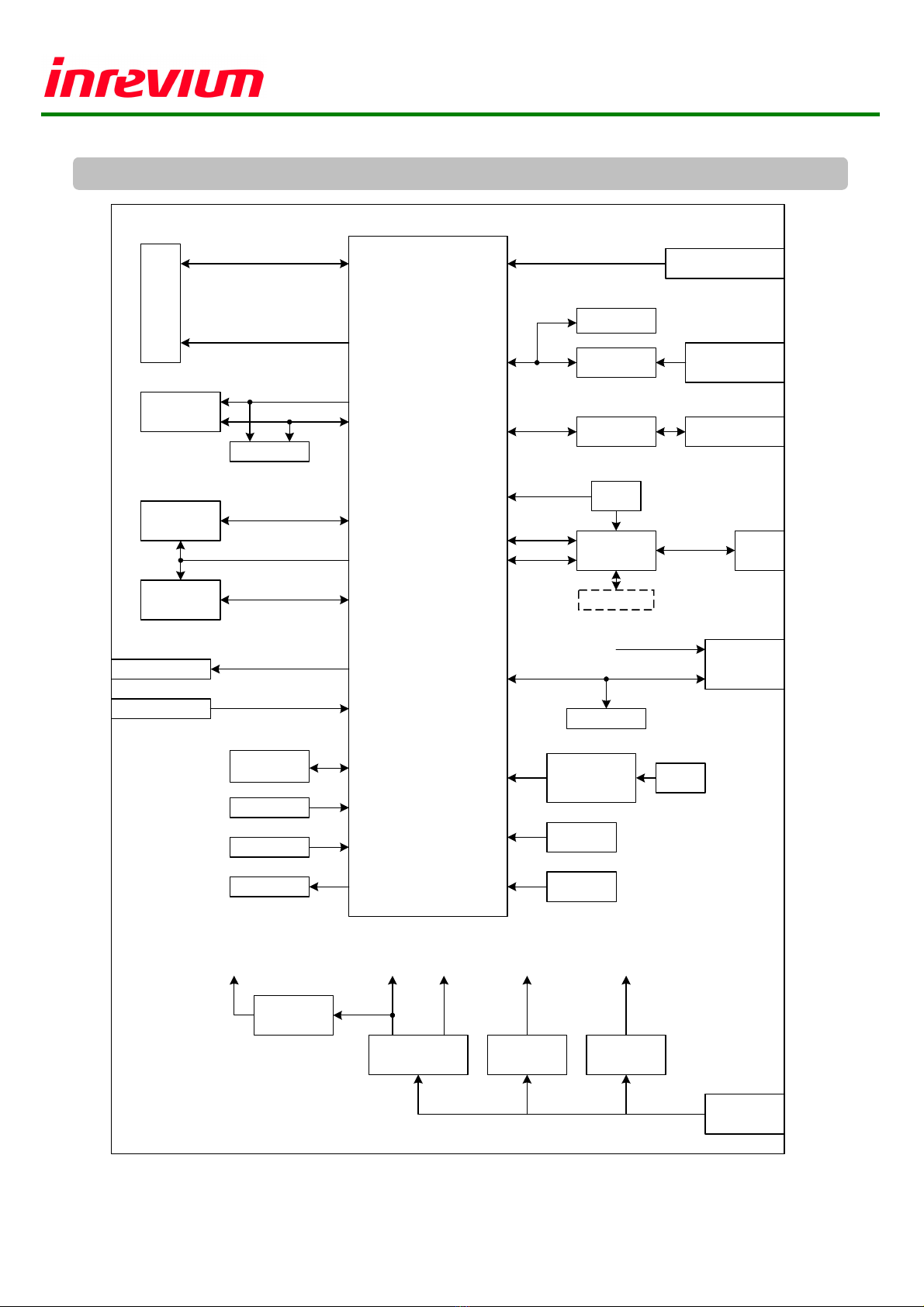
DDR2 SODIMM
DDR2
512M
LVDS Rx
Config Chip
TE7725PF
LTC1348 UART
9pin D-SUB
JTAG
PC4 &
PinHeader
LVDS OSC
(200MHz)
OSC
Socket×2
DIP SW×10
LED×10
Push SW×6
Virtex5
LX110
or
LX220
or
LX 0
1760pin
Data,DQS
ADR,CLK,Command
Data,DQS
ADR,CLK,Command
Genera
I/O
100pin×4
LTM4600 LTC3728L
LTC3413
1.0V1.8V3.3V0.9V
Power
Connector
C ock Synth.
ICS8430I-61
(133to400MHz)
OSC
16MHz
LAN9118 RJ45
LVDS Tx
F ash Rom
12V,3.3V,2.5V
Soft tuch CN
DDR2
512M
Data,DQS
DDR2
512M Data,DQS
ADR,CLK,Command
Soft tuch CN
LTM4600
EEPROM
OSC
25MHz
12V
20
PinHeader
Addr,
Data
Cont TD,RD
2.5V
JTAG
PC4 & PinHeader
5. Block Diagram
Figure.1 TB-5V-LX110/220/ 0-DDR2 Block Diagram

Sep
4, 2007 (Rev 2.1s) 6/26
TB-5V-LX110/220/ 0-DDR2Hardware User Guide Rev2.1s
LVDS I/O Power Setting P.11
LVDS I/O Connect P.27
10/100 Base Ethernet P.25
Power SW
Power Status LED 1.0V P.8
Genera I/O Pin Header P.40
User DipSW P.15
User LED P.16
Power Status LED 1.8V P.8
Power Status LED 0.9V P.8
DDR2 SDRAM Memory P.21
Power Status LED 3.3V P.8
Power Status LED 2.5V P.8
Config SW P.69
PC4 Connect P.56
JTAG Pin Header P.56
Config Setting SW P.51
Option I/O Connect P.31Option I/O Connect P.31
Soft Tough Connect P.41 Soft Tough Connect P.41
PLL Setting DipSW P.14
User PushSW P.15
RS-232C Port P.17
Virtex5 FPGA
DDR2 SDRAM SO-DIMM Socket P.18
PC4 Connect P.56
JTAG Pin Header P.56
Option I/O Power Setting P.9
Config Mode Setting P.68
OSC Socket P.13
Program LED P.51
VBATT_0 Leve Setting P.54
F ash Memory Area Setting SW P.52
6. External View
Figure.2 TB-5V-LX110/220/ 0-DDR2 board outline
7. Board Specification
Out side dimension : 250mm x 230mm
Board Layer : 12 Layers
Thickness : 1.6mm
Board Materia : Genera FR4
FPGA : XC5VLX110 or 220 or 330-1FF1760C
Configuration : TE7725PF (TED) and F ash memory: S29G128N(Spansion)
DDR2 SDRAM chip : EDE5116AHSE (32Mbit X 16 ELPIDA) 3 chips
Memory Modu e : DDR2 SDRAM SO-DIMM Socket (Up to 2GB)
LVDS I/O : 56 pins connector (I/O:22 pair) Tx, Rx
High speed I/O : 100 pins connector (I/O: 42 pins) x4
Mu ti-purpose I/O : 30 pins Pin-header (I/O: 20 pins) x1
Soft-touch connector : Soft-touch probe x5 (Agi ent Techno ogy)
10/100 Base Ethernet : RJ45 modu ar Jack
RS232C : Interface with PC

Sep
4, 2007 (Rev 2.1s) 7/26
TB-5V-LX110/220/ 0-DDR2Hardware User Guide Rev2.1s
AC ADAPTER 12V
Switch
LTC3728LEUH-1
LTM4600EV LTM4600EV
LTC3413EFE
1.0V 1.8V
0.9V
3.3V 2.5V
Vref Vin
FPGA
Core
FPGA
I/O Bank
3.3V
Device
FPGA
VCCAUX
I/O Bank
2.5V
Device
FPGA
I/O Bank
DDR2
SDRAM
FPGA
Vref
DDR2
Vref
VTT
8. Board Components
Power Connector and Power Module
Sing e 12V power is externa y supp ied from the AC adaptor that comes with the board.
Figure. AC Adopter connection
Power Supp y Connections
Figure.4 Power Supply Connection Diagram

Sep
4, 2007 (Rev 2.1s)
8/26
TB-5V-LX110/220/ 0-DDR2Hardware User Guide Rev2.1s
Power Status LED
Power Status LEDs (LED5, LED7, LED10, LED13 and LED19) indicate that the power supp y is
running norma y. Ensure that a Leeds are turned on, otherwise something is wrong with the board.
Switch off the power supp y since there may be a short circuit between the FPGA user circuit and
device.
Figure.5 Power Supply status LED location
12V LED
1.0V LED
1.8V LED
0.9V LED
3.3V LED
2.5V LED

Sep
4, 2007 (Rev 2.1s)
9/26
TB-5V-LX110/220/ 0-DDR2Hardware User Guide Rev2.1s
Bank26
(JP8)
Bank25
(JP10)
Option I / O 1 Option I/ O 2 Option I/ O 3 Option I/ O 4
Bank6
(JP6)
Bank4
(JP2)
Bank21
(JP9)
Bank 22
(JP7)
Power Voltage Selector for I/O connectors
It is possib e to se ect 2.5V or 3.3V for VCCO power vo tage of option I/O connectors.
■ Bank4, Bank6, Bank21, Bank22, Bank25, Bank26
Connected to: Option I/O connector
Set each jumper to the desired power vo tage (2.5V or 3.3V) in accordance with interface eve .
*JP1 is the jumper for Configuration Mode (P.68)
Figure.6 Jumper setting for power of Option I/O connector
Set power se ection using jumper (JP2, JP6, JP7, JP8, JP9, JP10) on board.
It has possibi ity to not be ab e to connect with an option board depending on the combination
across vo tage eve s.
It is described about the combination across vo tage setting of each jumper in Tab e 1.
Warning: Don’t set except the combination in Tab e.1 because of damage.
Figure.7 Allocation for FPGA Bank and Jumper setting
3.3V
Setting
2.5V
Setting
Sep
4, 2007 (Rev 2.1s)
10/26
TB-5V-LX110/220/ 0-DDR2Hardware User Guide Rev2.1s
Power Voltage Selector for LVDS connectors
It is possib e to se ect 2.5V or 3.3V for VCCO power vo tage of LVDS connectors.
■ Bank20, Bank24
Connected to: LVDS I/O connector
Set jumper to the desired power vo tage (2.5V or 3.3V) in accordance with interface eve using
JP3.
Figure.8 Jumper setting for selection of LVDS I/O connector
3.3V
Setting
2.5V
Setting

Sep
4, 2007 (Rev 2.1s)
11/26
TB-5V-LX110/220/ 0-DDR2Hardware User Guide Rev2.1s
Power Voltage Selector for I/O pin header connectors
It is possib e to se ect 2.5V or 3.3V for VCCO power vo tage of LVDS connectors.
■ Bank19
Connected to: Pin header I/O connector, User DIP switch, User Push switch
Set jumper to the desired power vo tage (2.5V or 3.3V) in accordance with interface eve using
JP12.
Figure.9 Jumper setting for selection of Pin header I/O connector
Pin header
2.5V
Setting
Pin header
3.3
V
Setting
Sep
4, 2007 (Rev 2.1s)
12/26
TB-5V-LX110/220/ 0-DDR2Hardware User Guide Rev2.1s
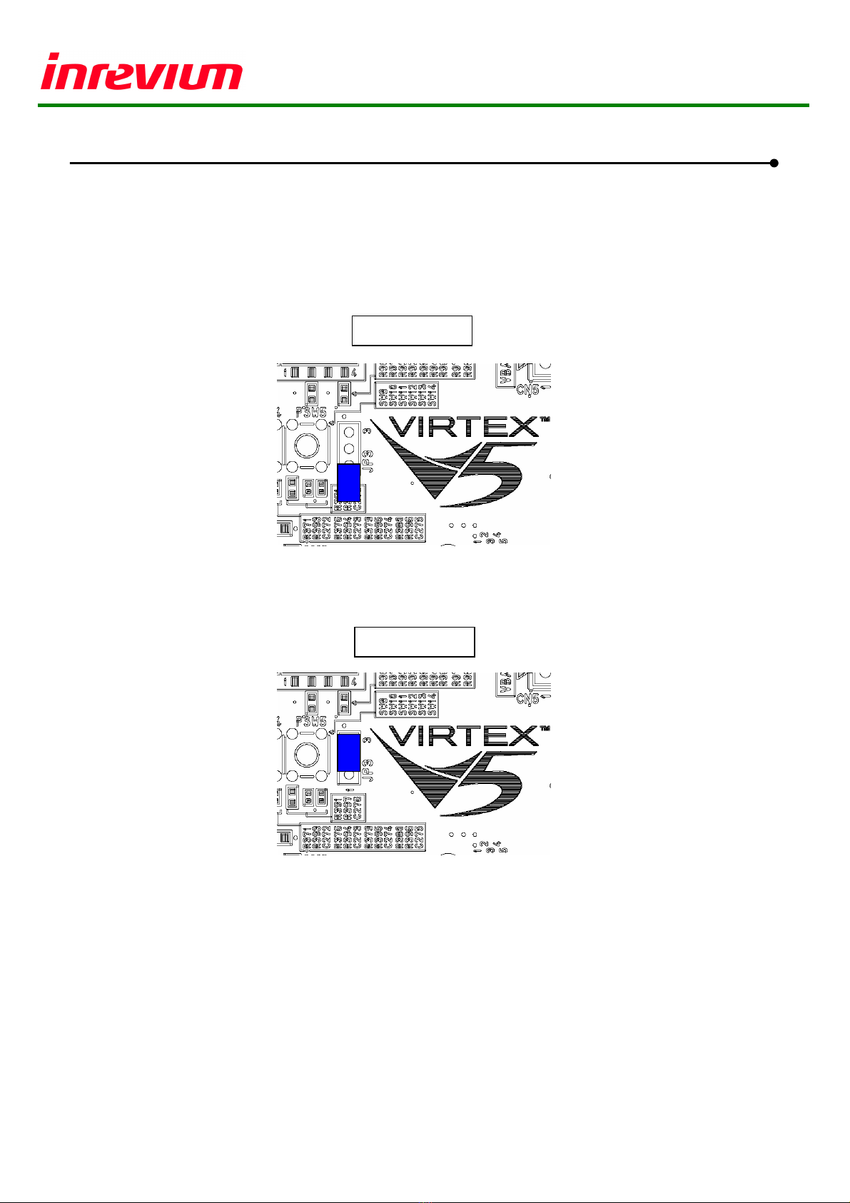
Oscillator
The board is provided with one differentia LV-PECL PLLIC (DIP switch setting for variab e frequency)
and two osci ator sockets that are connected to the FPGA’s GCLK pin.
Be sure to set the 16MHz osci ator that comes with the board to a correct pin position of the osci ator
socket (X1) that is connected to the PLLIC.
If an osci ator other than that provided with the board is used, se ect a 3.3V osci ator. Either DIP14
or DIP8 pin size osci ator package can be supported.
Note: There are 3.3-2.5V eve shift buffers between OSC socket (X3/X4) and FPGA.
Example of oscillator setting
Figure.10 How to insert an Oscillator
DIP 8Pin Type
DIP 14Pin Type

Sep
4, 2007 (Rev 2.1s)
1 /26
TB-5V-LX110/220/ 0-DDR2Hardware User Guide Rev2.1s
1
2
4
8
6
32
64
128
256
M0
M1
M2
M3
M4
M5
M6
M7
M8
250 0
1
0
1
1
1
1
1
0
1
0
0
0
251 1
1
0
1
1
1
1
1
0
1.5
1
0
0
252 0
0
1
1
1
1
1
1
0
2
0
1
0
253 1
0
1
1
1
1
1
1
0
3
1
1
0
* *
*
*
*
*
*
*
*
*
4
0
0
1
* *
*
*
*
*
*
*
*
*
6
1
0
1
* *
*
*
*
*
*
*
*
*
8
0
1
1
500 0
0
1
0
1
1
1
1
1
12
1
1
1
N2M N N0 N1
PLLIC (ICS84 0-61) Setting
DIP switches SW5 to SW7 are used to set output frequency of PLLIC.
Output frequency can be obtained in the fo owing formu a.
Fout = (fxtal/16)x(M/N)
Be sure to set it so that interna VCO frequency fvco((fxta /16)x M) is within a range of 250 - 500MHz.
*Ex) M=250/N=2 setting generates 125MHz c ock. ===> Fout = 16/ 6x250/2 = 125MHz
Table. ICS84 0-61 Setting
*Note: Va ue (“1” or “0”) of the setting
M0-M6, N0 and N2of DIP switches: When the setting of DIP switches are "ON", each va ue is
set to "1 (High)"
M7,M8 and N1 of DIP switches: When the setting of DIP switches are "ON", each va ue is set
to "0 (Low)"
See Tab e.4 DIP Switch Setting for re ationship between DIP switch setting and PLL output frequency
when a 16MHz osci ator that comes with the board is used.
Table.4 DIP Switch Setting
M0 M1 M2 M3 M4 M5 M6 M7 M8 N0 N1 N2
133 ON ON ON ON OFF OFF OFF OFF OFF ON OFF OFF
166 OFF ON OFF OFF ON ON ON OFF OFF ON OFF OFF
200 OFF OFF ON ON OFF ON OFF ON OFF ON ON OFF
266 ON ON ON ON OFF OFF OFF OFF OFF ON ON OFF
333.33 OFF OFF ON OFF ON ON ON OFF OFF ON ON OFF
SW7
Output freq.
(MHz)
SW5 SW6

Sep
4, 2007 (Rev 2.1s) 14/26
TB-5V-LX110/220/ 0-DDR2Hardware User Guide Rev2.1s
User DIP Switch
A 10bit DIP switch is connected to the I/O of FPGA. Set the switch to ON to set High.
The signa eve is changed 2.5 or 3.3V according to Pin Header.
Figure.11 DIP Switch Setting
Pushbutton Switch
Six pushbutton switches are connected to the I/O of FPGA. Whi e each switch is pushed, FPGA I/O is
set to High. The signa eve is changed 2.5 or 3.3V according to Pin Header.
Figure.12 User Push Switch
User LED
There are ten red LEDs and connected with FPGA. Each LED ights on when set to High.
Figure.1 User LED
ON: Output “High”
OFF: Output ”Low”
Sep
4, 2007 (Rev 2.1s) 15/26
TB-5V-LX110/220/ 0-DDR2Hardware User Guide Rev2.1s
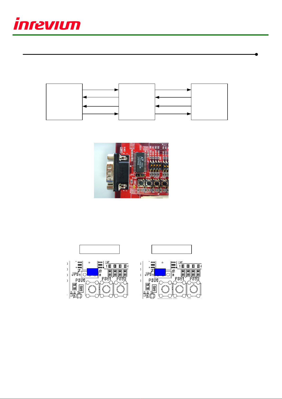
RS-2 2C Port
This connecter can transfer Tx/Rx data from user function and CPU program with connecting with PC.
(Then the cab e is used “Cross Cab e” that is avai ab e commercia y.)
Figure.14 RS-2 2C Block Diagram
Figure.15 RS-2 2C
RS232C Driver can set On/Off by Jumper SW.
Short between 2-3 of JP5 : On
Short between 1-2 of JP5 : Off
Figure.16 RS-2 2C Driver On/Off Setting
ON
OFF
FPGA
Virtex-5
RS232C
Driver
LTC1348
RS232C
Connector
9-pin D-Sub
RTS
RXD
CTS
TXD

Sep
4, 2007 (Rev 2.1s) 16/26
TB-5V-LX110/220/ 0-DDR2Hardware User Guide Rev2.1s
DDR2 SDRAM SO-DIMM Socket
DDR2 SO-DIMM socket is mounted on this board.
(It is possib e to use up to 2GB DDR2 SO-DIMM)
Figure.17 DDR2 SDRAM SO-DIMM Socket

Sep
4, 2007 (Rev 2.1s) 17/26
TB-5V-LX110/220/ 0-DDR2Hardware User Guide Rev2.1s
DDR2 SDRAM
512 M
(IC29)
DQ(16),DQS(8),/DQS (8)
Soft Touch CN
FPGA
Virtex-5
CAS,RAS,WE,CS,CKE,ODT
Address(14),DM(2),BA(3)
CK,/CK
DDR2 SDRAM
512 M
(IC30)
DQ(16),DQS(8),/DQS (8)
Address(14),BA(3)
CAS,RAS,WE,CKE,ODT
DM(2),CS
CK,/CK
DDR2 SDRAM
512 M
(IC31)
DQ(16),DQS(8),/ DQS(8)
DM(2),CS
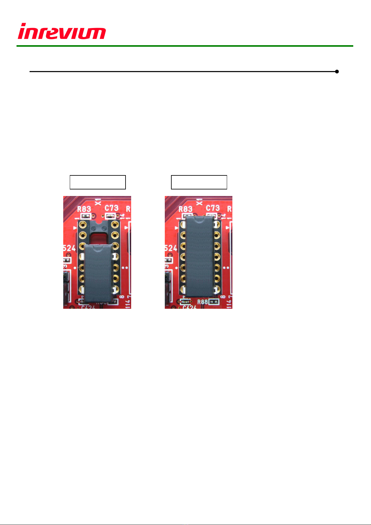
DDR2 SDRAM Memory Component
Three pieces of DDR2 SDRAM component (512Mb) is used on this board (Two Configurations).
The connection between FPGA and memories is shown ike Figure.19.
A so Soft-touch connector that is produced by Agi ent Techno ogy is mounted between FPGA and
IC29 so it’s possib e to confirm each signa using Agi ent’s Logic Ana yzer.
Figure.18 DDR2 SDRAM Component
Figure.19 Connection of DDR2 SDRAM Component
Sep
4, 2007 (Rev 2.1s) 18/26
TB-5V-LX110/220/ 0-DDR2Hardware User Guide Rev2.1s
10/100 Base Ethernet
Ethernet contro er (LAN9118) is mounted on this board so it is possib e to communicate
10/100Base Ethernet with PC via RJ-45 connector.
Figure.20 RJ-45 connector and Ethernet controller
LVDS I/O Connector
For high speed data access, two channe s (Tx/ Rx) of LVDS connectors are mounted on this board.
There are 20 pair of data ines and 2 pair of c ock ine for each channe .
A though signa eve is variab e to se ect 2.5V or 3.3V, it is possib e to se ect another I/O standard
not on y LVDS.
Figure.21 LVDS I/O Connector
High Speed Extension I/O Connector
For rea izing variab e interface, there are four connectors for option board shown by Figure.22.
It is possib e to change the signa eve to 2.5 or 3.3V according to connected interface.
Assuming the high speed image data input from an externa device, the board provides 5 LVDS pairs
for data, 2 LVDS pairs for c ock at differentia 100 ohm impedance and other signa ines at sing e 50
ohm impedance. It a so provides GND, VCC(2.5V,3.3V( and +12V power supp y.
Note: For differentia pair, refer in the fo owing tab e.
Figure.22 Option I/O Connector
RJ-45
LAN9118
Rx
Tx

Sep
4, 2007 (Rev 2.1s) 19/26
TB-5V-LX110/220/ 0-DDR2Hardware User Guide Rev2.1s
Multi-Purpose I/O Pin Header
It is possib e to change the signa eve to 2.5 or 3.3V according to connected interface.
Figure.2 Multi- Purpose I/O Pin Header
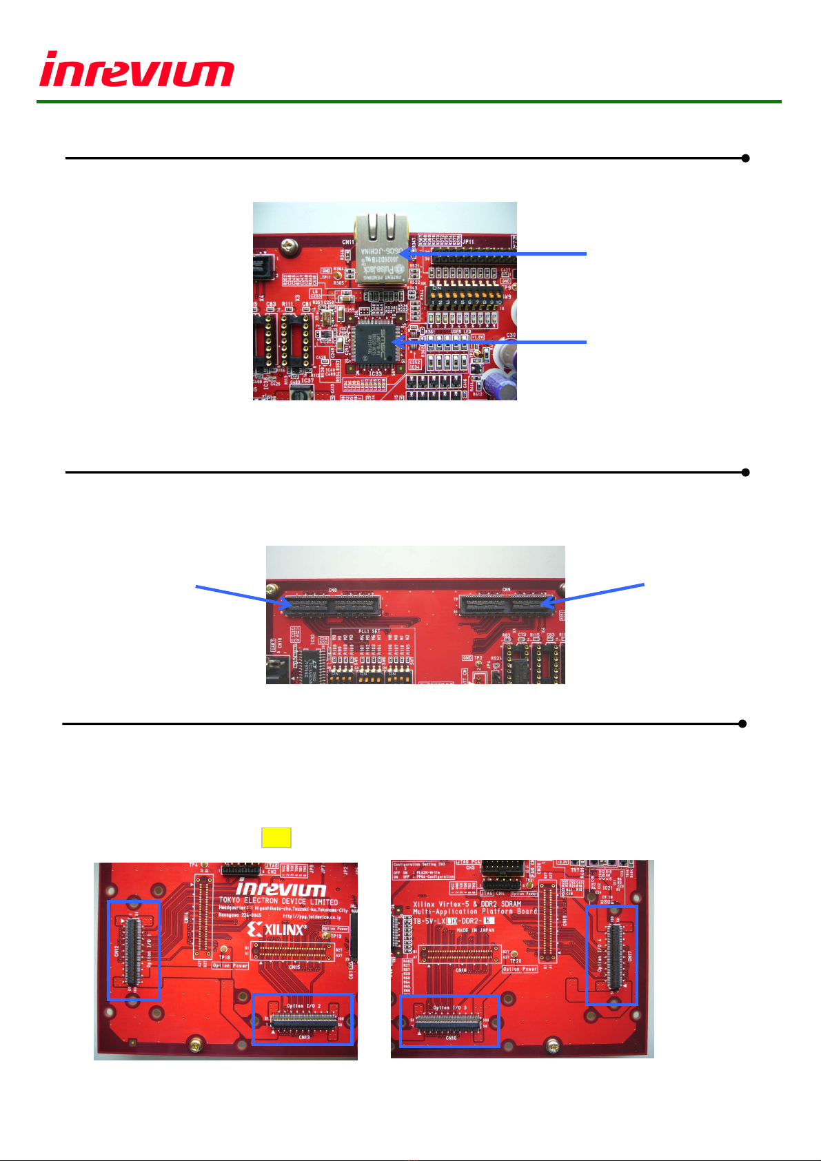
Soft-Touch Connector
Soft-Touch Connector produced by Agi ent Techno ogy is mounted between FPGA and DDR2
SDRAM (IC29), and between FPGA and Option I/O connectors (CN12, 13, 16, 17) on this board
as the fo owing picture.
Figure.24 Soft-Touch Connector

Sep
4, 2007 (Rev 2.1s) 20/26
TB-5V-LX110/220/ 0-DDR2Hardware User Guide Rev2.1s
Flash memory Sector Selection Setting
The setting of SW15 can se ect to a programming section of f ash memory. For this feature, it is
possib e to program mu tip e data and to se ect severa configuration data.
Figure. 1 Flash memory Sector Selection Switch (SW15)
Table.18 Configuration Setting
*Note: ‘0’ is switch OFF, ‘1’ is switch ON.
1 2 3 4 5
0 0 0 0 0 16Mbit F ash A Region(Top Sector)
1 0 0 0 0 32Mbit F ash A Region(Top Sector)
0 1 0 0 0 64Mbit F ash A Region(Top Sector)
1 1 0 0 0 32Mbit F ash ast Region 16Mbit(Top Sector)
0 0 1 0 0 128Mbit F ash A Region(Top Sector)
1 0 1 0 0 32Mbit F ash First Region 16Mbit(Top Sector)
0 1 1 0 0 128Mbit F ash 7/8,8/8Region 32Mbit(Top Sector)
1 1 1 0 0 128Mbit F ash 5/8,6/8Region 32Mbit(Top Sector)
0 0 0 1 0 256Mbit F ash A Region(Top Sector)
1 0 0 1 0 64Mbit F ash 4/4Region 16Mbit(Top Sector)
0 1 0 1 0 64Mbit F ash 3/4Region 16Mbit(Top Sector)
1 1 0 1 0 64Mbit F ash 2/4Region 16Mbit(Top Sector)
0 0 1 1 0 64Mbit F ash 1/4Region 16Mbit(Top Sector)
1 0 1 1 0 64Mbit F ash 3/4,4/4Region 32Mbit(Top Sector)
0 1 1 1 0 64Mbit F ash 1/4,2/4Region 32Mbit(Top Sector)
1 1 1 1 0 128Mbit F ash 5/8,6/8,7/8,8/8Region 64Mbit(Top Sector)
0 0 0 0 1 16Mbit F ash A Region(Bottom Sector)
1 0 0 0 1 32Mbit F ash A Region(Bottom Sector)
0 1 0 0 1 64Mbit F ash A Region(Bottom Sector)
1 1 0 0 1 32Mbit F ash ast Region 16Mbit(Bottom Sector)
0 0 1 0 1 256Mbit F ash ast Region 128Mbit(Top Sector)
1 0 1 0 1 32Mbit F ash First Region 16Mbit(Bottom Sector)
0 1 1 0 1 128Mbit F ash 3/8,4/8Region 32Mbit(Top Sector)
1 1 1 0 1 128Mbit F ash 1/8,2/8Region 32Mbit(Top Sector)
0 0 0 1 1 256Mbit F ash First Region 128Mbit(Top Sector)
1 0 0 1 1 64Mbit F ash 4/4Region 16Mbit(Bottom Sector)
0 1 0 1 1 64Mbit F ash 3/4Region 16Mbit(Bottom Sector)
1 1 0 1 1 64Mbit F ash 2/4Region 16Mbit(Bottom Sector)
0 0 1 1 1 64Mbit F ash 1/4Region 16Mbit(Bottom Sector)
1 0 1 1 1 64Mbit F ash 3/4,4/4Region 32Mbit(Bottom Sector)
0 1 1 1 1 64Mbit F ash 1/4,2/4Region 32Mbit(Bottom Sector)
1 1 1 1 1 128Mbit F ash 1/8,2/8,3/8,4/8Region 64Mbit(Top Sector)
SW15 F ash Memory Region
Table of contents
Other Inrevium Motherboard manuals


Popular Motherboard manuals by other brands


Advantech
Advantech ASMB-782 Startup manual

Asus
Asus F1A55-M LE R2.0 user manual

Texas Instruments
Texas Instruments TPA2050D4EVM user guide

VIA Technologies
VIA Technologies EPIA ME6000 - VIA Motherboard - Mini ITX Operation guidelines

Raisonance
Raisonance REva v3 user guide

Texas Instruments
Texas Instruments SN75LVCP600S user guide