Intel BP4S33AT User manual

INTEL OEM PRODUCTS AND SERVICES DIVISION PRELIMINARY - REV 0.1
Classic/PCI i486 Baby-AT Motherboard Technical Product Summary
•
Page
1
®
Technical Product Summary
Classic/PCI i486TM Baby-AT Motherboard
Models:
BP4S33AT
BP4D33AT
BP4D266AT
Preliminary Version 0.1
April, 1993
Order Number PRELIMINARY

INTEL OEM PRODUCTS AND SERVICES DIVISION PRELIMINARY - REV 0.1
Classic/PCI i486 Baby-AT Motherboard Technical Product Summary
•
Page
2
Intel Corporation makes no warranty for the use of its products and assumes no responsibility for any errors which may appear in this document nor
does it make a commitment to update the information contained herein.
Intel Corporation retains the right to make changes to these specifications at any time, without notice.
Contact your local sales office to obtain the latest specifications before placing your order.
The following are trademarks of Intel Corporation and may only be used to identify Intel products:
376i750MAPNET
Abovei860Matched
ActionMediai960MCS
BITBUSIntel287Media Mail
Code BuilderIntel386NetPort
DeskWareIntel387NetSentry
Digital StudioIntel486OpenNET
DVIIntel487OverDrive
EtherExpressIntelParagon
ETOXintel inside.Pentium
ExCAIntellecProSolver
Exchange and GoiPSCREADY-LAN
FaxBACKiRMXReference Point
FlashFileiSBCRMX/80
Grand ChallengeiSBXRxServer
iiWARPSatisFAXtion
ICELANDeskSnapIn 386
iLBXLANPrintStorage Broker
InboardLANProtectSuperTuned
i287LANSelectThe Computer Inside.
i386LANShellTokenExpress
i387LANSightVisual Edge
i486LANSpaceWYPIWYF
i487LANSpoolIntelTechDirect
MDS is an ordering code only and is not used as a product name or trademark. MDS is a registered trademark of Mohawk Data Sciences
Corporation.
CHMOS and HMOS are patented processes of Intel Corp.
Intel Corporation and Intel's FASTPATH are not affiliated with Kinetics, a division of Excelan, Inc. or its FASTPATH trademark or products.
TRADEMARK ACKNOWLEDGMENTS
ATI is a trademark of ATI Technologies Inc.
AutoCAD is a trademark of Autodesk Inc.
BAPCo and Sysmark92 are trademarks of the Business Applications Performance Corporation.
Cadvance is a trademark of ISICAD Inc.
Centronics is a trademark of Centronics Data Computer Corp.
IBM, MDA, MCGA, EGA, VGA, Personal System/2, PS/2, PC/XT and PC/AT are trademarks of International Business Machines.
Microsoft, MS-DOS, OS/2, Xenix and Windows are trademarks of Microsoft Corporation.
Novell is the trademark of Novell, Inc.
PolySwitch is a registered trademark of Raychem Corporation.
SCO is a trademark of Santa Cruz Operations, Inc.
SPEC, SPECratio, SPECint92 and SPECfp92 are trademarks of the Standard Performance Evaluation Corporation.
UNIX is a trademark of AT&T Bell Laboratories.
Western Digital is a trademark of Western Digital Corp.
All other trademarks are the property of their respective owners.

INTEL OEM PRODUCTS AND SERVICES DIVISION PRELIMINARY - REV 0.1
Classic/PCI i486 Baby-AT Motherboard Technical Product Summary
•
Page
3
Classic/PCI i486 Baby-AT Motherboard
Preliminary Technical Product Summary
Revision 0.1
Table of Contents
Introduction.........................................................................................................................................4
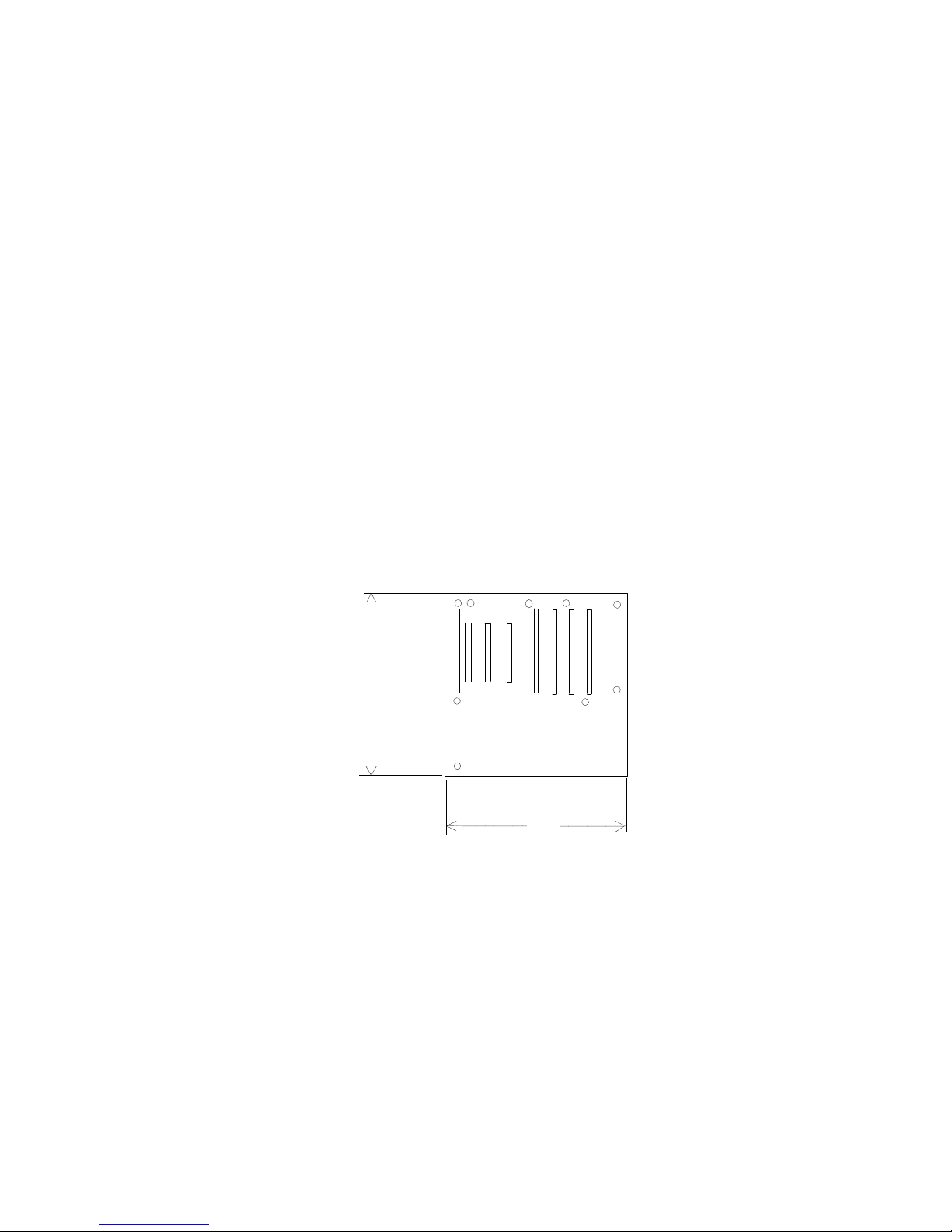
Baby-AT Form Factor...................................................................................................................4
Board Level Features..........................................................................................................................5
CPU..............................................................................................................................................5
Performance Upgrade ...................................................................................................................5
Second Level Cache......................................................................................................................5
System BIOS ................................................................................................................................5
PCI Auto-configuration Capability........................................................................................................ 5
Setup Utility......................................................................................................................................... 6
FLASH Implementation........................................................................................................................ 6
Upgrade Utility.....................................................................................................................................6
Flash User Area.................................................................................................................................... 7
Keyboard (and Mouse) Interface ...................................................................................................7
System Memory............................................................................................................................7
Core Chip Set ...............................................................................................................................7
82424TX Cache/DRAM/Controller (CDC) ...........................................................................................8
82423TX Data Path Unit (DPU)...........................................................................................................8
82378IB System I/O (SIO)....................................................................................................................8
Expansion Slots............................................................................................................................8
SMC 37C663 Super I/O Controller...............................................................................................8
Dallas DS12887 Real Time Clock, CMOS RAM and Battery........................................................8
Front Panel Connectors.................................................................................................................8
Security ........................................................................................................................................9
BIOS Password.....................................................................................................................................9
Setup Enable Jumper............................................................................................................................9
System Integration Features................................................................................................................10
Back panel Connections................................................................................................................10
Power Supply................................................................................................................................10
Appendices ..........................................................................................................................................11
Appendix A −User-Installable Upgrades......................................................................................11
System Memory.................................................................................................................................... 11
Performance Upgrade ...........................................................................................................................12
Qualified DRAM SIMMs .....................................................................................................................12
Appendix B −Jumpers..................................................................................................................13
Appendix C −BIOS Setup Options...............................................................................................14
Appendix D −BIOS Recovery ......................................................................................................15
Using the Upgrade Utility..................................................................................................................... 15
Recovery Mode.....................................................................................................................................15
Appendix E −Memory Map..........................................................................................................16
Appendix F −I/O Map..................................................................................................................17
Appendix G −Board Interrupts & DMA.......................................................................................18
Appendix H −Connectors.............................................................................................................19
AT Style Keyboard Port (J8L1 = Keyboard)..........................................................................................19
Optional PS/2 Style Keyboard, Mouse Ports (J8L2 = Keyboard, J9L1 = Mouse).................................... 19
Turbo LED Connector (J1A1)...............................................................................................................19
Hard Drive LED Connector (J1A2).......................................................................................................19
Key lock/Power LED Connector (J1B1)................................................................................................19
Speaker Connector (J1C1).................................................................................................................... 19
Turbo Switch Connector (J1C1B) .........................................................................................................19
Primary Power Connector (J9K1)..........................................................................................................20
Auxiliary (3.3V) Power Connector (J4H1)............................................................................................20
Parallel Port (J7J1)...............................................................................................................................20
Serial Ports (J7L2 = COM1, J7L1 = COM2)......................................................................................... 20
Reset Connector (J1B2)........................................................................................................................20

INTEL OEM PRODUCTS AND SERVICES DIVISION PRELIMINARY - REV 0.1
Classic/PCI i486 Baby-AT Motherboard Technical Product Summary
•
Page
4
Floppy Connector (J9F2) ......................................................................................................................21
IDE Connector (J9F3)...........................................................................................................................21
ISA Connector (J6G2, J6G1, J5G1, J4G1, J1G1) ..................................................................................22
PCI Connector (J3H1,J2H1,J1H1).........................................................................................................23
Appendix I −Baby-AT Chassis Suppliers .....................................................................................25
Appendix J −Environmental Standards........................................................................................26
Appendix K −Reliability Data......................................................................................................27
Appendix L −Software Driver Support.........................................................................................28
Appendix M −Qualified Peripherals.............................................................................................29
Appendix N −Customer Support..................................................................................................30
iPAN (Intel Product Assistance Network) .............................................................................................30
iPUB (Intel Product Update Bulletin) ...................................................................................................30
iPALS (Intel Phone Action Line Support) .............................................................................................30
FaxBack™...........................................................................................................................................30
Appendix O −Physical Dimensions..............................................................................................31
Board ...................................................................................................................................................31
Appendix P −Product Codes.........................................................................................................32
Boards..................................................................................................................................................32
Accessories...........................................................................................................................................32
Documentation .....................................................................................................................................32

INTEL OEM PRODUCTS AND SERVICES DIVISION PRELIMINARY - REV 0.1
Classic/PCI i486 Baby-AT Motherboard Technical Product Summary
•
Page
5
Introduction
The Classic/PCI i486 Baby-AT Motherboard delivers excellent, cost effective performance in a very affordable i486
platform. A wide range of CPU offerings provides immediate performance flexibility, and a single 238-pin blue
OverDriveReady ZIF (Zero Insertion Force) processor socket allows upgrades to higher performance in the future.
Additionally, by incorporating a second level, high performance cache and four SIMM sites for memory expansion to 128
MB, five ISA expansion connectors and three PCI connectors, the Classic/PCI i486 Baby-AT Motherboard is ideally
featured for expandable, performance sensitive desktop applications. The Classic/PCI i486 Baby-AT Motherboard will
excel in high end i486 Processor desktop PCs running existing compatible applications.
An easy upgrade path to higher CPU performance is built into the Classic/PCI i486 Baby-AT Motherboard. The processor
socket accepts either an i487SX to enhance performance with numeric intensive applications, or an OverDrive
Processor, Intel's upgrade component that doubles the speed of all i486 internal processes. Support for the next generation
OverDrive Processor, based on the PentiumCPU, protects today's investment in the Classic/PCI i486 Baby-AT
Motherboard.
The mini-Baby-AT board −with i486 CPU, cache, and integrated I/O −is the smallest PCI-based motherboard solution
on the market today that is upgrade able to an OverDrive processor based on Pentium CPU technology.
BABY-AT FORM FACTOR
The Classic/PCI i486 Baby-AT motherboard matches the Baby-AT standards well established in the PC industry, while
reducing the size from the full length (13") form factor. This Baby-AT industry standard specifies the maximum board
size, board mounting locations, and location for the keyboard connector, as well as expansion slot placement. The
Classic/PCI i486 Baby-AT meets all of these requirements while adding PCI expansion possibilities. Figure 1 illustrates
the Baby-AT form factor. A list of several chassis suppliers supporting the Baby-AT standard is included in Appendix
I.
9.1"
10.5"
Figure 1. Classic/PCI i486 Baby-AT Motherboard dimensions.

INTEL OEM PRODUCTS AND SERVICES DIVISION PRELIMINARY - REV 0.1
Classic/PCI i486 Baby-AT Motherboard Technical Product Summary
•
Page
6
Board Level Features
CPU
The Classic/PCI i486 Baby-AT motherboard has a wide price/performance range to meet a variety of customer needs.
Four base CPU options are available:
•an i486 SX running at 33 MHz;
•an i486 DX at 33 MHz;
•an i486 DX2 at 66 MHz; or
•a next generation i486 processor operating at 3.3V internally, and 33 MHz bus speed
The Classic/PCI i486 Baby-AT motherboard supports all of the functionality of the i486. Common features of the CPU
include backward compatibility with the 8086, 80286, and i386CPUs, burst mode bus cycles, and an on-chip 8 KB
cache. The cache is 4-way set associative, uses a write-through policy, and can be disabled via software.
The i486 DX CPU contains an on-chip numeric coprocessor to increase the speed of floating point operations. This
coprocessor is backward code-compatible with i387DX and i387 SX math coprocessors and complies with
ANSI/IEEE standard 754-1985. The i486 SX does not include the numeric coprocessor. The i486 DX2 incorporates
clock-doubling technology developed by Intel to offer the highest CPU performance available today.
PERFORMANCE UPGRADE
The Classic/PCI i486 Baby-AT motherboard incorporates a single 238-pin processor socket allowing easy upgrades to
CPU performance. All Classic/PCI i486 Baby-AT motherboards can be upgraded with an OverDrive Processor −
including future OverDrive Processors based on the Pentium CPU architecture. These upgrades will provide
significantly higher CPU performance and numeric capability. In addition, systems with a i486 SX/33 CPU can
improve floating point performance by installing an i487 SX/33 in place of the CPU. When replacing an i486 SX/33
CPU with an OverDrive Processor no jumper change are required; just power up and go!
SECOND LEVEL CACHE
In addition to the i486 CPU's internal cache, the Classic/PCI i486 Baby-AT motherboard was designed with a second
level cache using industry-standard SRAM. The 82424TX CDC includes a direct-mapped, write-back cache controller.
The motherboard includes four 32K x 8 20ns cache SRAM devices for a total of 128 KB cache memory.
SYSTEM BIOS
The Classic/PCI i486 Baby-AT Motherboard uses American Megatrends Incorporated (AMI) i486 CPU ROM BIOS,
which provides ISA compatibility. The system BIOS is stored in FLASH EEPROM, providing easy upgradability of
program code space from a floppy disk or a file downloaded from a BBS; BIOS upgrades will be available for download
from iPAN, the electronic bulletin board service of IntelTechDirect™. In addition to the AMI BIOS, the FLASH
memory also contains the PCI Auto-configuration utility, SETUP utility, Power-On Self-Tests (POST), and update
recovery code. For improved system performance, the Classic/PCI i486 Baby-AT Motherboard supports system BIOS
shadowing, allowing the BIOS to execute from 32-bit on-board write-protected DRAM instead of the slower 8-bit
FLASH devices. The Classic/PCI i486 Baby-AT BIOS sign-on during POST is along the bottom of the screen, and
contains information which identifies revision and type of BIOS. On the lower left is a four digit code which denotes
revision; first production units will display 0101, and as updates occur will roll the "minor revision number", i.e. 0102.
BIOS level and board identifier code is contained on the lower right side, and will be P00.AQ0 for the Classic/PCI i486
Baby-AT motherboard. As a note, A01 denotes Alpha revision 01, and B01 denotes Beta revision 01.
Further information on BIOS functions can be found in the IBM PS/2 and Personal Computer BIOS Technical
Reference published by IBM, and the ISA and EISA Hi-Flex AMIBIOS Technical Reference published by AMI and
available at most technical bookstores.
PCI AUTO-CONFIGURATION CAPABILITY
The PCI Auto-configuration feature provides a new level of user satisfaction. Simply plug a PCI add-in card into an
empty connector and turn the system on. The BIOS automatically configures interrupts, DMA channels, I/O space,
etc. This eliminates the requirement for adapter card jumper changes due to resource conflicts, and provides
unrivaled ease of use in a PC.

INTEL OEM PRODUCTS AND SERVICES DIVISION PRELIMINARY - REV 0.1
Classic/PCI i486 Baby-AT Motherboard Technical Product Summary
•
Page
7
The auto-configuration routine operates in conjunction with an ISA configuration utility. This utility enables the user
to specify the ISA options used, and ties into the PCI configuration software transparently to provide seamless add-in
card installation.
SETUP UTILITY
Classic/PCI i486 Baby-AT incorporates many commonly used system setup features into the FLASH EEPROM. The
BIOS SETUP Program has been enhanced and provides several new options to take advantage of the Classic/PCI
i486 Baby-AT Motherboard's new features. New options include:
•Auto configuration of IDE hard disks.
•Support for four IDE disk drives (primary and secondary)
•Serial Port 1 -- Enable/Disable
•Serial Port 2 -- Enable/Disable
•Parallel Port -- Enable/Disable, Bi-directional/Output only
•Cache/Shadow Memory Option -- Provides the user the option to assign a block of addresses below the 1 MB
boundary as non-shadowed, non-cached. Primarily used for expansion card ROM which causes timing issues
when shadowed and cached.
•ISA interrupts - Allows ISA interrupts IRQ9, IRQ10, IRQ15 to be assigned to add-in ISA adapters, thereby
informing the PCI configuration utility which interrupts not to use.
The setup utility is accessible only during the Power-On Self Test by pressing the <F1> key anytime after the POST
memory test has begun and before boot begins. For security purposes, access to SETUP can be disabled via a jumper
on the motherboard. The ROM-based setup allows the system configuration to be modified without opening the
system for most basic changes. Setup options are detailed in the Appendices.
FLASH IMPLEMENTATION
The Intel 28F001BXT 1 Mb FLASH component is organized as 128K x 8 (128 KB). The Flash device is divided into
five areas, as described in Table 2.
System Address
FLASH Memory Area
F0000H
FFFFFH
64 KB Main BIOS
EE000H EFFFFH 8 KB Boot Block (Not FLASH erasable)
ED000H EDFFFH 4 KB Parameter Block (used for PCI)
EC000H ECFFFH 4 KB Flash User Area
E0000H EBFFFH System BIOS
Table 1. Flash Memory Organization
The FLASH device resides in system memory in two 64 KB segments starting at E0000H, and is distributed in two
different organizations, depending on the mode of operation. In Normal Mode address line A16 is inverted,
switching the E000H and F000H segments so that the BIOS is organized as shown in the system address column
above. Recovery mode removes the inversion on address line A16, swapping the E000H and F000H segments so that
the 8 KB boot block resides at FE000H where the i486 expects the bootstrap loader to exist. This mode is only
necessary in the unlikely event that a BIOS upgrade procedure is interrupted, causing the BIOS area to be left in an
unusable state. For information on recovering the BIOS in the event of a catastrophic failure, refer to the Appendices.
UPGRADE UTILITY
FLASH memory brings new opportunities for distributing BIOS upgrades. Installing a new version of BIOS will no
longer require removal of the system cover and the replacement of EPROM's. Instead, the upgrade can be done
completely from a floppy diskette. Easy access to BIOS upgrades will be available through download able files on
the iPAN bulletin board.
Security is provided in two ways. First, the FLASH upgrade utility insures the upgrade BIOS matches the target
system to prevent accidentally installing a BIOS for a different type of system. Second, security to prevent
unauthorized changes to the BIOS is provided via a write protect jumper on the motherboard. The default setting is
to allow BIOS upgrades. A recovery jumper is provided to recover from the unlikely event of an unsuccessful BIOS
upgrade. It forces the ROM decode to access a 32 KB block of write protected code in the FLASH device that
facilitates recovery. The default value for this jumper (RV) is for "normal" mode (note: this jumper is not changed
during normal BIOS updates, it is used only if a problem is encountered).
The disk-based FLASH upgrade utility (FMUP.EXE; download able from iPAN) has three options for BIOS
upgrades:

INTEL OEM PRODUCTS AND SERVICES DIVISION PRELIMINARY - REV 0.1
Classic/PCI i486 Baby-AT Motherboard Technical Product Summary
•
Page
8
•The FLASH BIOS can be updated from a file on a disk;
•The current BIOS code can be copied from the FLASH EEPROM to a disk file as a backup in the event that an
upgrade cannot be successfully completed; and
•The BIOS in the FLASH device can be compared with a disk file to ensure the system has the correct BIOS
version.
FLASH USER AREA
Classic/PCI i486 Baby-AT supports a 4 KB programmable Flash User area located at ED000H-EDFFFH. A
programmer may use this area to display a customized message or to execute a small program. The Classic/PCI i486
Baby-AT BIOS accesses the user area just after completing the POST (Power-On Self-Test) if the setup option is
enabled. The flash user area may be updated by running the FMUP.EXE utility, which expects the update files to
have a .USR extension. Sample programs and instructions are in the file CLSUSER.ZIP on the iPAN bulletin board.
KEYBOARD (AND MOUSE) INTERFACE
An Intel 8742 surface mount micro controller contains the Phoenix Technologies' compatible keyboard/mouse
controller code. An AT style keyboard connector is located on the back panel side of the motherboard. The 5V line on
this connector is protected with a PolySwitch circuit which acts much like a fuse except that it re-establishes the
connection after an over-current condition is removed. While the PolySwitch eliminates the possibility of having to
replace a fuse, care should be taken to turn the system power off before installing or removing a keyboard. As a
manufacturing option, customers whose chassis will allow two PS/2 style connectors, one for mouse and one for
keyboard, can be supported by offering PS/2 configuration instead of AT. The 8742 micro controller code supports
Power-On/Reset (POR), network, and keyboard password protection. Network and keyboard passwords require
programs contained on the utility disk that ships with the system, the POR password is set via the SETUP program. In
addition, the keyboard controller provides for the following "HOT" key sequences:
•CTRL-ALT-DEL: System software reset. This sequence performs a software reset of the system by jumping to
the beginning of the BIOS code and running the POST operation, excluding memory tests.
•<TBD 1> and <TBD 2>: Turbo mode selection. <TBD 1> sets the system for de-turbo mode (emulation of an 8
MHz 80286 CPU using wait states) and <TBD 2> sets the system for turbo mode (its normal operation at 33
MHz). Changing the Turbo mode may be prohibited by an operating system or application software.
SYSTEM MEMORY
The Classic/PCI i486 Baby-AT Motherboard provides four 36-bit wide SIMM sites for memory expansion with
single/dual sided SIMM modules. The memory array is controlled by the Intel 82424TX CDC, and data buffering is
provided by an Intel 82423TX DPU. The four SIMM sites support 256K x 36, 512K x 36, 1M x 36, 2M x 36, 4M x 36
and 8M x 36 SIMM modules. Minimum memory size is 2 MB, and maximum memory size, using four 8M x 36
SIMM modules, is 128 MB.
Memory is always interleaved in two banks; therefore the SIMM sites must be stuffed in pairs. Memory timing is
designed for 70ns fast page devices, faster DRAMs will operate in the board but will provide no performance
improvement. Parity generation/checking is provided for each 8-bit byte.
SIMMs may be installed in combinations of two or four modules; each two SIMMs within an interleaved bank must be
of the same memory size and type (see the Appendix for a complete list of combinations). There are no jumper settings
required for the memory size configuration, the System BIOS automatically sizes memory and initializes the 82424TX
DRAM controller for appropriate DRAM configuration.
CORE CHIP SET
The core chip set is the Intel Saturn chip set, consisting of one 82424TX Cache/DRAM Controller (CDC), one
82423TX Data Path Unit (DPU) device, and one 82378IB System I/O (SIO) bridge chip. This document will outline the
general functionality, for more detailed information refer to the data sheet for the 82420 PCISet from Intel. The Saturn
chip set provides the following functions:
•CPU reset control
•CPU L1 cache control
•CPU burst mode control
•CPU interface control
•Integrated L2 write-back cache controller with tag comparator
•Page-mode DRAM controller

INTEL OEM PRODUCTS AND SERVICES DIVISION PRELIMINARY - REV 0.1
Classic/PCI i486 Baby-AT Motherboard Technical Product Summary
•
Page
9
•Burst memory read/write control logic
•Data bus conversion to PCI
•Parity generation/detection to memory
•AT-BUS direction control
•Chip select for keyboard controller and RTC
•Speaker control
•NMI logic
•Floating-point coprocessor interface
•Keyboard reset and gate A20 emulation logic
•DMA controller
•Interrupt controller
•Counters/Timers
82424TX CACHE/DRAM/CONTROLLER (CDC)
The 82424TX provides all control signals necessary to drive the DRAM array, including multiplexed address signals.
It also controls system access to memory and generates snoop controls to maintain cache coherency.
82423TX DATA PATH UNIT (DPU)
The 82423TX provides data bus buffering and dual port buffering to the memory array. Controlled by the 82424TX,
the 82423TX device adds one load to the PCI bus and performs all the necessary byte and word swapping required.
Memory and I/O write buffers are included in these devices.
82378IB SYSTEM I/O (SIO)
The 82378IB integrates seven 32-bit DMA channels, five 16-bit timer/counters, two eight-channel interrupt
controllers, NMI logic, refresh address generation, and PCI/ISA bus arbitration circuitry together onto the same
device.
EXPANSION SLOTS
The Classic/PCI i486 Baby-AT Motherboard contains support for up to seven populated expansion slots, offering ISA
and PCI connectors. These connectors include four ISA bus expansion slots, and two PCI expansion slots; the seventh
slot uses both an ISA connector and a PCI connector side by side, and can accept either an ISA or PCI adapter board
but not both together. The expansion cards are oriented perpendicular to the motherboard. All three PCI expansion
slots accept PCI master cards, fully supporting the PCI specification.
SMC 37C663 SUPER I/O CONTROLLER
Control for the integrated serial ports, parallel port, floppy drive and IDE hard drive interface is incorporated into a
single component, the SMC FDC37C663. This component provides:
•Two NS16C552 compatible UARTs (with FIFO support)
•IBM and Centronics compatible bi-directional parallel port controller
•Industry standard floppy controller (with 2.88 MB floppy support)
•IDE hard disk decode and chip select
Header connectors are available near the back of the board for cabling these options. The serial ports can be enabled as
COM1 and COM2 or disabled. The parallel port can be enabled via the SETUP program as LPT1 or disabled, and can
be set as bi-directional or output only when enabled.
DALLAS DS12887 REAL TIME CLOCK, CMOS RAM AND BATTERY
The Real Time Clock (RTC) is implemented using a Dallas DS12887 device. The DS12887 is accurate to within 13
minutes/year and requires no external support (the battery and oscillator are integrated into the device). The
component is soldered into the board (the internal battery has an estimated lifetime of ten years).
The RTC can be set via the BIOS SETUP Program. CMOS memory supports the standard 128-byte battery-backed
RAM, fourteen bytes for clock and control registers, and 114 bytes of general purpose non-volatile CMOS RAM. All
CMOS RAM is reserved for BIOS use. The CMOS RAM can be set to specific values or cleared to the system default
values using the BIOS SETUP program. Also, the CMOS RAM values can be cleared to the system defaults by using a
hardware jumper. The appendices contain a list of jumper configurations.

INTEL OEM PRODUCTS AND SERVICES DIVISION PRELIMINARY - REV 0.1
Classic/PCI i486 Baby-AT Motherboard Technical Product Summary
•
Page
10
FRONT PANEL CONNECTORS
A connector (J1C1) is provided for installing a speaker. The speaker provides error beep code information during the
Power-On Self Test if the system cannot use the video interface. The Classic/PCI i486 Baby-AT product guide contains
beep and error code information.
Connectors J1B2, J1B1, J1C1B, and J1A2, J1A1 supply front panel connections to Reset, Key lock, and Turbo
switches, and hard disk and turbo LEDs, respectively.
SECURITY
Security features are incorporated into the Classic/PCI i486 Baby-AT system BIOS.
BIOS PASSWORD
A BIOS password feature provides security during the boot process. A password can be entered using the Setup
utility and must be re-entered prior to disk boot each time the system is reset. The password can be changed at the
password prompt by entering <old password> / <new password> / <new password> <enter>. The password also can
be cleared by entering <old password> / <enter>. If the password is forgotten, it can be cleared by turning off the
system and setting jumper PW to the right. After the system has finished the Power-On Self Test, turn the system off
and reset jumper PW to the left. This allows the user access to the password feature, but with the forgotten password
cleared.
SETUP ENABLE JUMPER
A jumper on the baseboard controls access to the BIOS Setup utility. By setting jumper SE to the right, the user is
prevented from accessing the Setup utility during the Power-On Self Test or at any other time.

INTEL OEM PRODUCTS AND SERVICES DIVISION PRELIMINARY - REV 0.1
Classic/PCI i486 Baby-AT Motherboard Technical Product Summary
•
Page
11
System Integration Features
BACK PANEL CONNECTIONS
The back panel provides external access to the keyboard controller integrated on the Classic/PCI i486 Baby-AT
motherboard. Figure 4 shows the back panel connections.
Keyboard connector
Figure 2. Classic/PCI i486 Baby-AT Back panel
POWER SUPPLY
The Classic/PCI i486 Baby-AT board could be powered by a 200 watt switch able power supply, providing
power for onboard resources, add-in cards, and peripherals.
DC Voltage Max. Continuous
Current Peak Current
15 Seconds Minimum
Current Load
+5V 18.5A 18.5 2.5A
-5V 0.9A 0.9A 0A
+12V 4.6A 9.5A 0.5A
-12V 0.5A 0.5A 0A
Table 2. Classic/PCI i486 Baby-AT Current Requirements
Table 2 lists the current used by system resources. This information is preliminary and is provided only as a guide for
calculating approximate total system power usage with additional resources added.
Resource Typical Power
Classic/PCI i486 Baby-AT baseboard, 16 MB (8 MB in each
of two banks), 128K cache 50 Watts
Teac 3½" Floppy drive 1.7 Watts
Table 3. Current Use by System Resources (Preliminary)

INTEL OEM PRODUCTS AND SERVICES DIVISION PRELIMINARY - REV 0.1
Classic/PCI i486 Baby-AT Motherboard Technical Product Summary
•
Page
12
Appendices
APPENDIX A
−
USER-INSTALLABLE UPGRADES
SYSTEM MEMORY
Table A-1 shows the total system memory based on the listed combinations of SIMMs in the four SIMM sockets.
SIMM 1,2 (Bank 0)
SIMM Type (Amount) SIMM 3,4 (Bank 1)
SIMM Type (Amount) Total System Memory
256K X 36 (1 MB) Empty 2 MB
256K X 36 (1 MB) 256K X 36 (1 MB) 4 MB
256K X 36 (1 MB) 512K X 36 (2 MB) 6 MB
256K X 36 (1 MB) 1M X 36 (4 MB) 10 MB
256K X 36 (1 MB) 2M X 36 (8 MB) 18 MB
256K X 36 (1 MB) 4M X 36 (16 MB) 34 MB
256K X 36 (1 MB) 8M X 36 (32 MB) 66 MB
512K X 36 (2 MB) Empty 4 MB
512K X 36 (2 MB) 256K X 36 (1 MB) 6 MB
512K X 36 (2 MB) 512K X 36 (2 MB) 8 MB
512K X 36 (2 MB) 1M X 36 (4 MB) 12 MB
512K X 36 (2 MB) 2M X 36 (8 MB) 20 MB
512K X 36 (2 MB) 4M X 36 (16 MB) 36 MB
512K X 36 (2 MB) 8M X 36 (32 MB) 68 MB
1M X 36 (4 MB) Empty 8 MB
1M X 36 (4 MB) 256K X 36 (1 MB) 10 MB
1M X 36 (4 MB) 512K X 36 (2 MB) 12 MB
1M X 36 (4 MB) 1M X 36 (4 MB) 16 MB
1M X 36 (4 MB) 2M X 36 (8 MB) 24 MB
1M X 36 (4 MB) 4M X 36 (16 MB) 40 MB
1M X 36 (4 MB) 8M X 36 (32 MB) 72 MB
2M X 36 (8 MB) Empty 16 MB
2M X 36 (8 MB) 256K X 36 (1 MB) 18 MB
2M X 36 (8 MB) 512K X 36 (2 MB) 20 MB
2M X 36 (8 MB) 1M X 36 (4 MB) 24 MB
2M X 36 (8 MB) 2M X 36 (8 MB) 32 MB
2M X 36 (8 MB) 4M X 36 (16 MB) 48 MB
2M X 36 (8 MB) 8M X 36 (32 MB) 80 MB
4M X 36 (16 MB) Empty 32 MB
4M X 36 (16 MB) 256K X 36 (1 MB) 34 MB
4M X 36 (16 MB) 512K X 36 (2 MB) 36 MB
4M X 36 (16 MB) 1M X 36 (4 MB) 40 MB
4M X 36 (16 MB) 2M X 36 (8 MB) 48 MB
4M X 36 (16 MB) 4M X 36 (16 MB) 64 MB
4M X 36 (16 MB) 8M X 36 (32 MB) 96 MB
8M X 36 (32 MB) Empty 64 MB
8M X 36 (32 MB) 256K X 36 (1 MB) 66 MB
8M X 36 (32 MB) 512K X 36 (2 MB) 68 MB
8M X 36 (32 MB) 1M X 36 (4 MB) 72 MB
8M X 36 (32 MB) 2M X 36 (8 MB) 80 MB
8M X 36 (32 MB) 4M X 36 (4 MB) 72 MB
8M X 36 (32 MB) 8M X 36 (8 MB) 128 MB
Table A-1. SIMM Memory Stuffing Options

INTEL OEM PRODUCTS AND SERVICES DIVISION PRELIMINARY - REV 0.1
Classic/PCI i486 Baby-AT Motherboard Technical Product Summary
•
Page
13
PERFORMANCE UPGRADE
There are several CPU upgrade paths. If you have an i486 SX processor, you can upgrade it with an Intel487 SX, an
i486 DX processor, an i486 DX2, or an OverDrive Processor (including Pentium processor-based OverDrive
components, when available). Systems with an i486 DX can be upgraded with i486 DX2 or OverDrive components,
and an i486 DX2 can be upgraded with the Pentium CPU-based OverDrive component when available. Upgrading
requires removing the current CPU from the 238-pin ZIF socket on the system board. The upgrade processor is
plugged into the socket and the system powered up; it's that easy. When the next generation i486 processors which
require 3.3V are available, they can also be used to upgrade the board; in this case, Jumpers CPUVCC must be
changed to provide the 3.3V to the processor. Intel487 and OverDrive components are available from Intel's Personal
Computer Enhancement Division. For the location of the nearest Intel dealer, phone 1 (800) 538-3373.
Just Look for the Blue ZIF Socket!
QUALIFIED DRAM SIMMS
Vendor Part Number Size (configuration)
Toshiba THM361010AS-70
Toshiba THM361020AS-70
Samsung KMM5361000A-7
Samsung KMM5361000B-7
Hitachi HB56D136SBS-7A
Micron MT9D136M-7
MTI Z124MBK36A-70I1
MTI Z124MBK36B-70I1
MTI Z124MBK36R-70IN
Table A-2. Sampling of memory DRAM SIMM Vendors

INTEL OEM PRODUCTS AND SERVICES DIVISION PRELIMINARY - REV 0.1
Classic/PCI i486 Baby-AT Motherboard Technical Product Summary
•
Page
14
APPENDIX B
−
JUMPERS
All the configuration jumpers on Classic/PCI i486 Baby-AT motherboard are the three pin, two position type. These sit
side by side in a 2x3 jumper block. The jumper description below assumes a particular point of reference in viewing
the motherboard. Position the board or system so that the CPU and Cache Rams are at the front nearest you, the Dram
SIMMs should be to the right. All functional jumpers have a two-letter indicator as shown in the table. Use these
indicators to locate and position the jumpers for your configuration. Some jumpers can be positioned top or bottom,
(bottom is towards the front of the board) others left or right.
INDICATOR DESCRIPTION DEFAULT
CP Cache Present Jumper. Jumper to the top position if no Cache Ram is
installed in the Board.
Jumpered to the bottom indicates Cache Ram is installed in the board.
Bottom
RV Recovery Jumper. Jumper to top for normal operation
Jumper to the bottom for BIOS RECOVERY MODE. Top
FI IDE Paddle Card Jumper. Jumper to top to indicate PCI IDE card is installed
in slot J3H1.
Jumpered to the bottom for normal on board IDE operation.
Bottom
BW BIOS Write Jumper. Jumper to the top to disable all writes to Flash EPROM.
Jumpered to the bottom allows for Flash EPROM Updates. Bottom
CPUVCC CPUVCC Jumpers. These jumpers are not user configurable. Moving
them can result in damage to the CPU!!
Left is for 5 volt CPU operation.
Right is for 3.3 volt operation of 5 volt tolerant CPUs. All four jumpers must be
positioned to the same side.
Left
CL Color/Mono Jumper. Jumpered to the left is for MGA operation.
Jumpered to the right is for color graphics adapters. Right
CM Clear CMOS Jumper. Jumper to the left will force CMOS to be CLEARED.
Jumper to the right for normal operation. Right
SE Setup Enable Jumper. Jumper to the left to allow setup to be enabled during
Boot-Up.
Jumper to the right to disable setup during Boot-up.
Left
PW Password Jumper. Jumper to the left for normal operation.
Jumper to the right to clear the password that was previously selected. Left
Table B-1. Classic/PCI i486 Baby-AT Jumper Description
Figure B-1. Classic/PCI i486 Baby-AT Jumper Locations

INTEL OEM PRODUCTS AND SERVICES DIVISION PRELIMINARY - REV 0.1
Classic/PCI i486 Baby-AT Motherboard Technical Product Summary
•
Page
15
APPENDIX C
−
BIOS SETUP OPTIONS
TBD

INTEL OEM PRODUCTS AND SERVICES DIVISION PRELIMINARY - REV 0.1
Classic/PCI i486 Baby-AT Motherboard Technical Product Summary
•
Page
16
APPENDIX D
−
BIOS RECOVERY
The Classic/PCI i486 Baby-AT incorporates an AMI system BIOS on a FLASH component. FLASH BIOS allows easy
upgrades without the need to replace an EPROM. The upgrade utility fits on a floppy diskette and provides the
capability to save, verify, and update the system BIOS. The upgrade utility can be run from a hard drive or a network
drive, but no memory managers can be installed during upgrades.
The latest upgrade utility and BIOS code are available in the public section of the iPAN bulletin board.
USING THE UPGRADE UTILITY
If the utility is obtained from iPAN, UNZIP the archive and copy the files to a bootable MS-DOS 3.3, 4.01, 5.0, or
6.0 bootable diskette. Reboot the system with the upgrade diskette in the bootable floppy drive and follow the
directions in the easy to use menu-driven program.
RECOVERY MODE
In the unlikely event that a FLASH upgrade is interrupted catastrophically, it is possible the BIOS may be left in an
unusable state. Recovering from this condition requires the following steps (be sure a power supply has been attached
to the board, and a floppy drive is connected as drive A:):
1. Move jumper RV to the bottom position.
2. Install the bootable upgrade diskette into drive A:
3. Reboot the system.
4. Because of the small amount of code available in the non-erasable boot block area, no video is available to direct
the procedure. The procedure can be monitored by listening to the speaker and looking at the floppy drive LED.
When the system beeps and the floppy drive LED is lit, the system is copying the recovery code into the FLASH
device. As soon as the drive LED goes off, the system can be turned off.
5. Reset jumper RV to the top position.
6. Leave the upgrade floppy in drive A: and turn the system on.
7. Continue with the original upgrade.

INTEL OEM PRODUCTS AND SERVICES DIVISION PRELIMINARY - REV 0.1
Classic/PCI i486 Baby-AT Motherboard Technical Product Summary
•
Page
17
APPENDIX E
−
MEMORY MAP
Address Range (Deci-
Address Range (hex)
Size
Description
16384K-32768K
1000000-2000000
16384K
Extended Memory
16256K-16383K FE0000-FFFFFF 128K System & Video BIOS Copy
1024K-16255K 100000-FDFFFF 15232K Extended Memory
960K-1023K F0000-FFFFF 64K AMI System BIOS
952K-959K EE000-EFFFF 8K FLASH Boot Block (Available as HIMEM)
948K-951K ED000-EDFFF 4K User FLASH Area (available as HIMEM if no user info is here)
928K-947K E8000-ECFFF 20K AMI Setup Program (disable via setup pre-boot only; with this
896K-927K E0000-E7FFF 32K Video BIOS (when installed)
800K-895K C8000-DFFFF 96K Available Hi DOS Memory(open to the ISA bus)
768K-799K C000-C7FFF 32K Optional VGA BIOS
736K-767K B8000-BFFFF 32K VGA Display Memory (not available to ISA bus)
704K-735K B0000-B7FFF 32K VGA & Mono Display Memory (HIMEM w/ QEMM)(not available to
640K-703K A0000-AFFFF 64K VGA Display Memory (not available to the ISA bus)
639K 9FC00-9FFFF 1K Extended BIOS Data (moveable by QEMM, 386MAX)
512K-638K 80000-9FBFF 127K Extended conventional
0K-511K 00000-7FFFF 512K Conventional
Table E-1. Classic/PCI i486 Baby-AT Memory Map

INTEL OEM PRODUCTS AND SERVICES DIVISION PRELIMINARY - REV 0.1
Classic/PCI i486 Baby-AT Motherboard Technical Product Summary
•
Page
18
APPENDIX F
−
I/O MAP
Address Range (hex) Size (Decimal) Description
0000 - 000F
16 bytes
SIO - DMA 1
0020 - 0021 2 bytes SIO - Interrupt Controller 1
0040 - 0043 4 bytes SIO - Timer 1
0048 - 004B 4 bytes SIO - Timer 2
0060 1 byte Keyboard Controller Data Byte
0061 1 byte SIO - NMI, speaker control
0064 1 byte Keyboard Controller, CMD & STATUS Byte
0070, bit 7 1 bit SIO - Enable NMI
0070, bits 6:0 7 bits SIO - Real Time Clock, Address
0071 1 byte SIO - Real Time Clock, Data
0073 1 byte Reserved - Board Configuration
0075 1 byte Reserved - Board Configuration
0078 1 byte SIO - BIOS Timer
0080 - 008F 16 bytes SIO - DMA Page Register
00A0 - 00A1 2 bytes SIO - Interrupt Controller 2
00C0 - 00DE 31 bytes SIO - DMA 2
00F0 1 bytes Reset Numeric Error
0170 - 0177 8 bytes Secondary IDE Channel
01F0 - 01F7 8 bytes Primary IDE Channel
0278 - 027B 4 bytes Parallel Port 2
02F8 - 02FF 8 bytes On-Board Serial Port 2
0376 1 byte Secondary IDE Channel Command Port
0377 1 byte Secondary IDE Channel Status Port
0378 - 037F 8 bytes Parallel Port 1
03BC - 03BF 4 bytes Parallel Port x
03E8 - 03EF 8 bytes Serial Port 3
03F0 - 03F5 6 bytes Floppy Channel 1
03F6 1 bytes Primary IDE Channel Command Port
03F7 (Write) 1 byte Floppy Channel 1 Command
03F7, bit 7 1 bit Floppy Disk Change Channel 1
03F7, bits 6:0 7 bits Primary IDE Channel Status Port
03F8 - 03FF 8 bytes On-Board Serial Port 1
0CF8 1 byte PCI Configuration Space Enable
0CF9 1 byte De-turbo Mode Enable
C000 - C0FF 256 bytes 82424TX Configuration Registers
C200 - C2FF 256 bytes 82378IB Configuration Registers
Table F-1. Classic/PCI i486 Baby-AT I/O Address Map

INTEL OEM PRODUCTS AND SERVICES DIVISION PRELIMINARY - REV 0.1
Classic/PCI i486 Baby-AT Motherboard Technical Product Summary
•
Page
19
APPENDIX G
−
BOARD INTERRUPTS & DMA
Interrupt Request
System Resource
NMI
Parity Error
0Reserved, Interval Timer
1Reserved, Keyboard buffer full
2Reserved, Cascade interrupt from slave PIC
3Serial Port 2
4Serial Port 1
5Parallel Port 2
6Floppy
7Parallel Port 1
8Real Time Clock
9User available
10 User available
11 User available
12 On-board Mouse Port if enabled, else user available
13 Reserved, Math coprocessor
14 IDE if enabled
15 User available
Table G-1. Classic/PCI i486 Baby-AT Interrupt Map
DMA Channel
Data Width
System Resource
0
8-or 16-bits
Open
18-or 16-bits Open - Normally used for LAN
28-or 16-bits Floppy
38-or 16-bits IDE
4Reserved - Cascade channel
516-bits Open
616-bits Open
716-bits Open
Table G-2. Classic/PCI i486 Baby-AT DMA Map

INTEL OEM PRODUCTS AND SERVICES DIVISION PRELIMINARY - REV 0.1
Classic/PCI i486 Baby-AT Motherboard Technical Product Summary
•
Page
20
APPENDIX H
−
CONNECTORS
AT STYLE KEYBOARD PORT (J8L1 = KEYBOARD)
Pin Number
Signal Name
1
Clock
2Data
3No Connect
4 Ground
5Vcc (fused)
Table H-1. AT Style Keyboard Connector Pin Definition
OPTIONAL PS/2 STYLE KEYBOARD, MOUSE PORTS (J8L2 = KEYBOARD, J9L1 = MOUSE)
Pin Number
Signal Name
1
Data
2No Connect
3 Ground
4Vcc (fused)
5Clock
6No Connect
Table H-2. PS/2 Mouse and Keyboard Connector Pin Definition
TURBO LED CONNECTOR (J1A1)
Pin Number
Signal Name
1
PULL_UP_330
2LED_TURBO-
Table H-3. Turbo LED Connector Pin Definition
HARD DRIVE LED CONNECTOR (J1A2)
Pin Number
Signal Name
1
PULL_UP_330
2HD ACTIVE-
3 Key
4 PULL_UP_330
Table H-4 Fixed Disk LED Connector Pin Definition
KEY LOCK/POWER LED CONNECTOR (J1B1)
Pin Number
Signal Name
1
LED_PWR
2 Key
3 Ground
4KEY LOCK
5 Ground
Table H-5. Key lock Connector Pin Definition
SPEAKER CONNECTOR (J1C1)
Pin Number
Signal Name
1
SPKR_DAT
2 Key
3No Connect
4+5V Vcc
Table H-6. Speaker Connector Pin Definition
TURBO SWITCH CONNECTOR (J1C1B)
Pin Number
Signal Name
1
TURBO
2 Ground
3No Connect
Table H-7. Turbo Switch Connector Pin Definition
PRIMARY POWER CONNECTOR (J9K1)
This manual suits for next models
2
Table of contents
Other Intel Motherboard manuals

Intel
Intel Atom Pine Trail-D525 User manual

Intel
Intel I440 LX User manual

Intel
Intel CV700A User manual

Intel
Intel D865PERL User manual

Intel
Intel BOXDG965WHMKR User manual

Intel
Intel Enano-8523 User manual

Intel
Intel D945PWM User manual

Intel
Intel AI5VG User manual

Intel
Intel P35 User manual

Intel
Intel BLKDH57JG Configuration guide

Intel
Intel Celeron 1047UE/847 User manual

Intel
Intel PMB-601LF User manual

Intel
Intel D2550MUD2 User manual

Intel
Intel DH57DD User manual

Intel
Intel D945PWM User manual

Intel
Intel BLKDG31GL Configuration guide

Intel
Intel D815EGEW User manual

Intel
Intel DX79SI User manual

Intel
Intel 41210 User manual

Intel
Intel BLKDP67BG Configuration guide