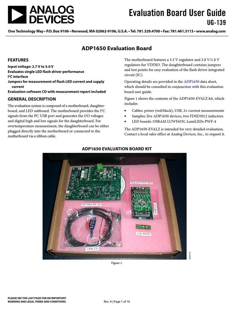
Evaluation Board User Guide UG-360
Rev. 0 | Page 3 of 8
SETTING UP THE EVALUATION BOARD
INPUT CONFIGURATION
On the bottom center of the PCB are four 2-pin headers, H3 to H6.
These are used to connect the input audio signals to the amplifier.
If the input audio signals are differential, use the two center pins
of H3 and H4 (INL+ and INL−) for left channel audio and the two
center pins of H5 and H6 (INR+ and INR−) for the right channel
audio. In this case, connect either the top or the bottom pin to
the source/signal ground.
For single-ended audio inputs, the input lines are connected
only to the pins of H3 (INL+ and GND) and H5 (INR+ and GND).
Jumpers are placed in H4 and H6, shorting INL− and INR− to
ground.
Alternatively, single-ended stereo audio may be supplied by
connecting a standard ⅛ inch stereo plug to the J7 input
instead of connecting it to H3 and H5.
SHUTDOWN MODE
The 3-pin headers, H9 and H12, are used to tie SDNL and SDNR
to either GND or AVDD, to enable or disable the left and right
channels of the amplifier. Placing a jumper between
the center pin and AVDD puts the in normal operation.
Placing the jumper between the center pin and GND shuts down
the so that only a minimum current (about 10 μA)
is drawn from the power supply.
SSM3302
SSM3302
SSM3302
GAIN CONFIGURATION
Two headers, H2 and JP6, control the SSM3302 analog gain. By
placing a jumper across the two pins of H2, the GAIN pin of
the amplifier can be connected to GND or AVDD. Three jumper
settings are used: between the center pin and the top pin (AVDD),
between the center pin and the bottom pin (GND), and no
jumper (open).
A 47 kΩ resistor, R18, is inserted between the GAIN pin and
the H2 jumper. Placing a jumper on JP6 shorts across this
resistor (R18), allowing two extra gain levels.
Gain settings between 9 dB and 24 dB are available. See Table 1
for the gain configuration details.
Table 1. Gain Configuration
Gain (dB) JP6 H2 Configuration
9 Short GND Short GAIN pin to GND
12 Open GND GAIN pin through 47 kΩ to GND
15 Open Open GAIN pin unconnected
18 Open AVDD GAIN pin through 47 kΩ to AVDD
24 Short AVDD Short GAIN pin to AVDD
OUTPUT CONFIGURATION
The output terminals, J3 to J6, provide convenient attachment
points for speakers or other load devices with standard banana
connectors. In addition, 2-pin, 0.100 inch headers are provided.
Because the SSM3302 does not typically require any external audio
band LC output filtering due to a low noise modulation scheme,
a low cost, high performance, common-mode choke-based filter
is installed on the evaluation board for EMI suppression. For
optimal performance measurement, remove this filtering by
inserting 0 Ω links or a thick wire short across L1 and L2. In
this case, leave the filter capacitors, C16 to C18 and C26 to C28,
unpopulated.
To safeguard against system radiated emission failure, especially
if the speaker cable length exceeds 20 cm, it may be necessary to
include an output filter. The recommended filter uses common-
mode chokes, L1 and L2, in the output paths, plus capacitors,
C16 to C18 and C26 to C28, to couple the output terminals to
ground. A schematic of this configuration is shown in Figure 4,
with recommended values for the filter components given. The
recommended common-mode chokes are listed in Tabl e 2.
Alternatively, inductors may be used instead of common-mode
chokes; however, the distortion performance is slightly worse at
high power. If inductors are used, they must be used in pairs,
with two inductors replacing each common-mode choke. A
summary of the recommended inductors is shown in Table 3.
For optimal total harmonic distortion (THD) and signal-to-noise
ratio (SNR) performance as specified in the SSM3302 data sheet,
remove the output filters and short across L1 and L2.
POWER SUPPLY CONFIGURATION
The banana jacks, J1 and J2, are used to power the board. Care
must be taken to connect the dc power with correct polarity and
voltage. Reverse polarity or overvoltage may damage the board
permanently. Permissible supply voltages range from 7 V to 18 V;
higher voltages may damage the amplifier.
ANALOG SUPPLY
In addition to the 7 V to 18 V power supply, a 5 V analog supply
(AVDD) must be present to power the input stage and modulator.
The SSM3302 amplifier has an internal regulator to provide a
clean 5 V rail for this purpose; alternatively, an external supply
can be used.
When the REGEN pin is pulled high (between 1.35 V and 5.5 V),
the internal regulator is enabled, and the chip begins to operate.
If the REGEN pin is pulled low, the regulator is enabled, and an
external supply must be connected to H1. Do not connect the
REGEN pin directly to PVDD, because this will damage the
regulator.
On the SSM3302 evaluation board, the voltage drop from the
power indicator LED, D2, is used to provide the logic high level
for REGEN. To enable the regulator, tie the center pin of JP3 to
the upper pin, V_LED. To disable the regulator, tie it to GND.

